Note: Descriptions are shown in the official language in which they were submitted.
- 1 - 1 3 3 5 5 39
This invention relates to sensors for use in
biological, biochemical and chemical testing and in
particular to immunosensors used to monitor the
interaction of antibodies with their corresponding
antigens.
When antibodies are immobilised on a surface, the
properties of the surface change when a solution
containinQ a corresponding antigen is brought into
contact with the surface to thus allow the antigen to
bind with the antibody. In particular, the change in the
optical properties of the surface can be monitored with
suitable apparatus.
The phenomenon of surface plasmon resonance (5PR)
can be used to detect minute changes in the refractive
index of the surface as the reaction between the antigen
and the antibody proceeds. Surface plasmon resonance is
the oscillation of the plasma of free electrons which
exists at a metal boundary. These oscillations are
affected by the refractive index of the material adjacent
the metal surface and it is this that forms the basis of
the sensor mechanism. Surface plasmon resonance may be
achieved by using the evanescent wave which is generated
when a p- polarised light beam is totally internally
reflected at the boundary of a medium, e.g. glass, which
has a high dielectric constant. A paper describing the
technique has been published under the title "Surface
plasmon resonance for gas detection and biosensing" by
Lieberg, Nylander and !undstrom in Sensors and Actuators,
Vol. 4, page 299. In order that the invention may be
better understood, several embodiments thereof will now
be described by way of example only and with reference to
the accompanying drawings in which:
~ igures 1 and 2 are diagrams of known experimental
arrangements for demonstrating the surface plasmon
resonance effect;
.
~ ~ s~
~_ - la - 1 335539
Figure 3 is a diagrammatic side view of an
embodiment of a sensor according to the present
invention;
Figures 4 and 5 are ray diagrams showing the optical
geometry of a prism and a rectangular slab; and
Figure 6 is a view similar to Figure 3, showing an
alternative embodiment.
Illustrated in Figure 1 of the accompanyiny drawings
is a diagram of the equipment described in this paper. A
~0 beam 1 of light is applied from a laser source (not
shown) onto an internal surface 2 of a glass body 3. A
detector lnot shown) monitors the internally reflected
beam 4. Applied to the external . . . . . . . . . . . .
. ~,
2 1 3 3 5 ~ 3 9
surface 2 of glass body 3 is a thin film S of metal,
for example gold or silver, and applied to the film 5
is a further thin film 6 of organic material containing
antibodies. A sample 7 containing antigen is brought
into contact with the antibody film 6 to thus cause a
reaction between the antigen and the antibody. If
binding occurs the refractive index of the layer 6 ~ill
change owing to the increased size of the antibody
molecules and this change can be detected and measured
using the surface plasmon resonance technique, as will
now be explained.
Surface plasmon resonance can be experimentally
observed, in the arrangement of Figure l, by varying
the angle of the incident beam l and monitoring the
intensity of the internally reflected beam 4. At a
certain angle of incidence the parallel component of
the light momentum will match with the dispersion for
surface plasmons at the opposite surface 8 of the metal
film. Provided that the thickness of metal film S is
20 chosen correctly there will be an electromagnetic
coupling between the glass/metal interface at surface 2
and the metal/antibody interface at surface 8 which
results in surface plasmon resonance and thus an
attenuation in the reflected beam 4 at that particular
25 angle of incidence. Thus, as the angle of incidence
of beam l is varied, surface plasmon resonance is
observed as a sharp dip in the intensity of the
internally reflected beam 4 at a particular angle of
incidence. The angle of incidence at which resonance
30 occurs is affected by the refractive index of the
material against the metal film 5 - i.e. the antibody
layer 6 - and the angle of incidence correspondins tG
resonance is thus a direct measure of the state of the
reaction between the antibody and the antigen.
35 Increased sensitivity can be obtained by choosing an
angle of incidence half way down the reflectance dip
3 - 1 3 3 5 5 3 9
curve, where the response is substantially linear, at
the beginning of the antibody/antigen reaction, and
then maintaining that angle of incidence fixed and
observing changes in the intensity of the reflected
5 beam 4 with time.
Known systems of the type described with
reference to Figure l utilise a prism as the glass body
3. A diagram showing this arrangement is given in
Figure 2 which is simply an experimental set up
10 intended to demonstrate surface plasmon resonance.
The prism is shown under reference 8 and has applied to
its undersurface a thin film ~ of metal. Light l from
a laser source (not shown) is incident on the prism
where it is refracted at point 9 before entering the
15 prism. The internally reflected beam 4 is likewise
refracted (at point 10) upon exiting from the prism.
One problem with the prism is that, as the
angle of incidence is changed, either by moving the
source, or rotating the prism, or both, the point on
20 surface 2 at which the incoming beam is incident moves.
~ecause of inevitable variations in the metaI film 5
and the coating 6 of antibody, the angle of incidence
which results in resonance changes as this movement
occurs, which in turn introduces a further variable
25 factor into the measurement and thus makes comparisons
between the initial, unbound, state and the bound state
of the antibody layer 6 less accurate.
In the present invention this difficulty is
eliminated or reduced by replacin~^ the essentially
30 refractive optics of known arran~ements by reflective
optics. By reflective optics as used herein, we mean
that light from the light source is 2ppl ied to the
transparent block in which surface plasmon resonance is
generated via at least one reflecting element such as
35 d ~i rror.
In order to create the conditions necessary for
. .. . , . , , . . . . . . , = .
~, ~ 4 ~ 1335539
surface plasmon resonance to occur, it is still
necessary to provide a block of transparent material,
usually glass, through which the light is passed in
order to create a surface at which internal reflection
5 takes place. However, as will be explained, this block
could be any shape because the refraction which this
block inevitably introduces can either be ignored
(because it is insignificant), or can be compensated
for in the reflective optics. As an example, the block
10 may take the form of a thin glass plate, such as are used
for microscope slides, onto one surface of which is
applied the metal and the antibody film in the
manner illustrated in Figure 1. Incoming light is
applied to the opposite surface and refracts through it
15 at the interface. If the angle of incidence is
correct, internal reflection will take place in such a
way as to produce surface plasmon resonance at the
metal/glass interface, as explained above, and the
emergent beam leaves the glass plate from the same
20 surface on which it originally entered, another
refraction taking place at the point of exit. Provided
that the glass plate is thin enough, these two
refractions do not adversely affect the operation of the
device. However, if the plate is not so thin, or if
25 the block is some other shape - for example prismatic
such as shown in Figure 2 - then refraction at the
glass/air interface, particularly in connection with
the incoming beam, can cause problems of the type
mentioned above. Provided reflective optics are used,
30 as proposed for the present invention- then refractions
can be compensated for by tailoring the optics in such
a way that, whatever the angle of incidence within the
range c.~ interest about the dip, the light will always
be incident on the metal/~lass interface at a
35 particular point. It is believed that the optics may
be tailored for any reasonable shape of alass including,
_ - 5 ~ 1 335539
as has been mentioned, flat plates, or prisms, and may by
the same token be used in conjunction with the hemicylin-
drical and hemispherical blocks used in the apparatus
described in our corresponding Canadian Patent Application
574,605, or in conjunction with the optical waveguides
(e.g. fibre optics) described in our corresponding Canadian
patent application 588,360.
Although the radiation used to obtain surface
plasmon resonance is described throughout this specifica-
tion as being light, in theory surface plasmon resonance
effects should be obtainable using electromagnetic radi-
ation of other frequencies. However in practice the
radiation concerned is likely to be within or near the
optical region, and the word light should be interpreted
accordingly.
The reflecting element is preferably such as to
bring the light to a focus at the point of incidence on the
glass/metal interface. Thus with a "solid" input beam of
reasonable width, the input beam effectively becomes
several beams incident upon the glass/metal interface over
a range of angles. The arrangement is such that the range
of angles span the angle of dip corresponding to surface
plasmon resonance. The corresponding internally reflected
beam is likewise effectively several beams and may be
monitored by a large area detector, or by an array of
angularly spaced detectors positioned to collect the whole
emergent beam. Thus the detectors can encode the informa-
tion from the whole of the dip within milliseconds.
The use of a "solid" beam, such as described
above, and as described in our co-pending Canadian applica-
tions 574,605 and 588,360, means that the light incident on
the glass/metal interface effectively spans a range of
angles and thus, if this is centred around that angle of
incidence which is necessary to
~ - 6 1335539
produce surface plasmon resonance, then the whole dip
can be "seen" simultaneously by the detector.
One problem with this is that, in order to
simultaneously look at the whole of the output beam
from such apparatus, a detector having a large
sensitive area must be provided. In addition, because
the information in the beam is distributed on a spatial
basis, it is necessary that the detector incorporates
some form of x - y positional information, as well as a
simple intensity measurement. Such detectors do exist,
in the form of "large area" detectors and multi-
detector arrays, but they are very expensive.
In a preferred embodiment of the present
invention, we use just a single narrow beam, and means
are provided for causing its angle of incidence at the
glass/metal interface to scan across a range of angles
of incidence such as is suitable for viewing the dip
resulting from surface plasmon resonance. If the
centre angle of such movement is chosen, for example,
20 to be the angle at which surface plasmon resonance
takes place, then the whole dip can be rapidly
scanned. To effect scanning, scanning means are used
to scan the output of the radiation source backwards
and forwards about a small arc before it is applied to
25 the focussing means. Alternatively, the scanning means
may be operable to cause a continuous 360 sweep of the
output of the radiation source - somewhat in the manner
of the rotating light from a lighthouse - and to mask
off all but a small arc of this sweep, which small arc
30 is thence applied to the focussing means. The
focussing means is operable to ensure that the scanning
beam is incident on the glass/metal interface at
substantially the same point whatever the instantaneous
scanning angle might be.
The scanning means may, for example take the
form of a plane mirror which is oscillated backwards
~ 7 - 1 335539
and forwards at a frequency of, for example 50Hz.
Alternatively, the scanning means may be such as to
cause continuous rotation of the mirror at, for
example, 50 r.p.s., thus resulting in the 360 swept
beam referred to above. The mirror may be moved by a
suitable motor and mechanical interconnection.
Suitable examples are synchronous motors, DC servo
motors and the like. The circuitry associated with the
motor outputs a strobe pulse so that the detector which
looks at the output beam - i.e. the beam which has been
internally reflected at the glass/metal interface - is
able, at any one instance of time, to identify the
particular angle of incidence at which the input light
is incident at the glass/metal interface. It will be
seen that the information in the input light about the
SPR reflectance dip is not obtained on a spatial basis,
but on a time basis by synchronising the scanning of
the input beam with the information output from the
detector to build up a "picture" of the dip as the
reaction between the antigen and the antibody proceeds.
Because only a relatively narrow beam is being
used, only a detector having a small active area is
needed, and these are very cheap. Since the output
beam will move as the input beam is scanned, it is
25 necessary, at the output side, to provide means for
bringing the output beam into a path which will ensure
that it is intercepted by the detector, whatever the
angle it leaves the glass/metal interface. This may be
readily achieved with- suita~le output optics. In an
3o alternative embodiment the detector may take the form
of a large area detector which is positioned to
intercept the output beam whatever its angle of
incidence. Since the detector would only have to
provide an intensity reading, and not an indication of
35 the beam x - y position, the detector can be
implemented quite cheaply, for example, in the form of
`f - - 8 l 335539
an amorphous silicon device.
The mirror used to scan the input beam can
additionally be used to cause the beam to scan in other
planes to enable multiple tests to be carried out
simultaneously. The scanning to move the beam about
the SPR dip, as described above, is essentially a
single-plane effect, the beam being incident at the
glass/metal interface at a single point which is
stationary. By moving the point of incidence, multiple
tests can be carried out, in effect, simultaneously
because the movement of the beam is very fast compared
with the progress of the test or tests.
In one embodiment, the mirror is caused to scan
additionally in a plane at right angles to the plane of
scanning to produce, in effect, a second scanning
movement. Instead of producing a single stationary
point of incidence, a line of incidence is produced,
caused by the point of incidence moving along the line
as the second scanning movement of the mirror takes
20 place. By using a multiple mirror arrangement, further
lines, parallel to the first, can be scanned thus
giving, in effect, two dimensional raster scanning of
an area. All that is now necessary is to divide up the
metal and antibody layers across the line or area being
25 scanned to enable separate tests to be carried out at
each such divided area. Depending upon the particular
sample feeding arrangements used, this enables the
effective simultaneous testing of a number of different
analytes within a given specimen, or a number of
3o separate specimens. The separate divided areas may
each have the same antibody or may have different
antibodies, and one or more may have no antibodies at
aIl, to act as "reference" areas.
The scanning arrangements may be such as to
35 cause continuous scanning of the point of incidence
across the line or area to be tested, in which case the
~f ~ 9 1335539
circuitry associated with the apparatus will be
designed to ascertain, on a time basis, just where the
point of incidence is at any one time (and therefore
which area is being tested) and relate this to the
output of the detector. As an alternative, the
scanning may be such as to cause the point of incidence
to "hover" over each area to be tested for a time
sufficient to enable scanning across the dip to be
effected at that point before passing on to the next.
The shaping of the reflecting element can
additionally be carried out in order to compensate for
other irregularities, in particular refraction, as the
light enters the glass block, in order to ensure that
the light is always incident on as near as possible a
single spot on the glass/metal interface at which
surface plasmon resonance occurs. It is possible to
obtain reflective surfaces having very complex shapes
using precision cutting machinery under computer
control. For example diamond machined alu-inium can be
used as the reflective surface. In practice, with the
requirement for the beam to be focussed at the
glass/metal interface, the reflective surface will be
generally concave with a shape close to parabolic. The
exact shape, however, in two dimensions ~ill be
25 determined also by the nature and shape of the glass
block, this shape being derived by suitable computer
programming.
If desired, a characteristic modulation may be
impressed on the electromagnetic radiation so that
30 synchronous detection may be used to ensure that
signals at the detector relating to the desired
reflected radiation are adequately distinguishable from
those undesired output signals relating to extraneous
radiation or other noise sources that can affect the
35 detector. Such modulation is particularly desirable
when using a single large-area detector.
~-- - 10 - 1335539
Although the layer applied to the metal film is
described herein as an antibody layer for use in
immunoassays, it will be seen that any sensitive layer
whose refractive index changes upon an event occurring
can be used to thus provide a sensitive detector having
a wide variety of applications in the fields of
biology, biochemistry and chemistry. The material
comprising the sensitive layer may be specific to a
particular entity within the sample or may be non-
specific (i.e. may interact with several species ofentity within the sample). Examples of specific
materials include recognition molecules such as the
aforementioned antibodies which will specifically bind
an analyte of interest within the sample, DNAIRNA
probes which will bind with their complements in the
sample liquid, or lectins, glycoproteins or enzyme
substrates, all of which are capable of recognising and
binding with the other partner in a bimolecular
recognition pair.
Examples of non-specific materials include
hydrophobic materials, for example in the form of a
monolayer of phospholipid-type molecules to capture
amphipathic molecules, or hydrophilic materials ~hich
would capture polysaccharides. Indeed, it has been
25 found that the surface of the metal film itself can
form an effective non-specific binding material.
Silver or gold surfaces will bind proteins or
polynucleotides such as DNA or RNA without the need for
any further coating and, in this case a separate
30 sensitive layer is effectively dispensed with
altogether, and the surface of the metal film used
directly for the capture of entities within the sample
to be tested.
The metal film material is commonly silver or
35 gold, usually applied by evaporation. The film needs
to be as uniform as possible in order to cater for
1 1 - 1 3 3 55 3 9
minute movement in the point of incidence of the
incoming beam. It is assumed that a structured metal
film will give the best resonance and there are various
ways in which the glass body can be pretreated to
improve the performance of the metal film and in
particular to control the natural tendency of such
films to form discontinuous islands:-
1. Immersion in molten nitrates and other molten
salts. This has the effect of introducing ions into
the surface in a manner which can be structured and
which can act as foci for island formation.
2. Ion bombardment of cold or hot glass to
introduce nucleating sites. The removal of the more
mobile ions has been demonstrated to reduce the
thickness at which the evaporated film becomes
continuous.
3. Electroless plating or electroplating over
lightly evaporated films (0 to 100 angstroms thick).
Electroless plated films survive to a greater thickness
than evaporated films and could form more stable nuclei
for subsequent coating.
4. Evaporating on to electroless plated films.
The electroless plated films have a stronger tendency
to an island structure and to bigger islands with
25 greater spacing than evaporating films. This could be
of advantage in tuning light of a prescribed
wavelength.
Coating performance can also be improved by:-
1. Controlling the glass surface temperature
3o during coating. Using a higher temperature substrate
increases the islands' size and the spacing between
them and conversely.
2. Evaporating in the presence of a magnetic or
electrostatic field or electron emission device to
35 control the ion content of the vapour stream. The
state of charge of the substrate is known to affect the
- 12 - l 3 3 5 5 3 9
island structure.
3. Controlling the angle of incidence of the evaporated
vapour stream relative to the glass surface. The
mobility of the evaporated atoms and hence their ability
to form bigger islands is greater when the momentum of
the atoms relative to the ~lass surface is increased.
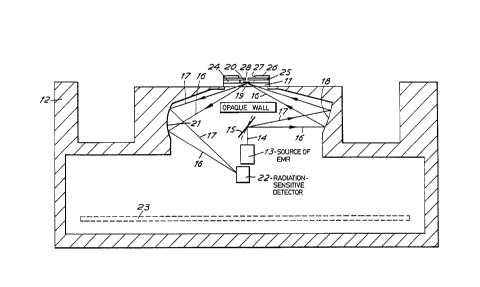
Referring to Figure 3, the apparatus comprises a
~lass slide 11 of transparent material such as ~lass or
quartz attached on a housing 12. A source 13 of
tO electromagnetic radiation produces a collimated input
beam 14 of electromagnetic radiation. The frequency of
the radiation must be such as to result in the generation
of surface plasmon waves and in practice will be within
or near the visible re~ion. Suitable sources include a
helium neon laser or an infra red diode laser, but an
ordinary light source, with suitable filters and
collimators could be used.
A rotatable mirror 15 is used to scan the beam
backwards and forwards between the limit positions shown
by the beams t6, 17 whose ray patterns are traced
through the apparatus. With the mirror in the . . . . .
- 13 - 1 335539
position indicated by the solid line, the limit beam 16
results; with the mirror in the position indicated by
the dotted line, the limit beam 17 results. The mirror
is moved by a motor (not shown) energised in such a way
as to cause the beam to continuously scan between the
limit positions 16 and 17. The mirror 15 may be driven
by a synchronous motor or DC servo motor or similar at
a rotation speed typically of 50HZ giving a scan period
in the millisecond region. The beam from the mirror 15
is reflected off a generally concave reflecting surface
18 and is incident at a point 19 on the upper surface
of the slide 11. This upper surface is formed with a
metal film layer on top of which is an antibody or
other sensitive layer, arranged in the manner illustrated
in Figure 1. The combined metal film/antibody layer is
shown under reference 20.
Radiation which is internally reflected at point 19
passes out of the slide and is reflected by a further
generally concave reflecting surface 21 into a
radiation sensitive detector 22 which gives an
electrical output signal for analysis by associated
circuitry mounted on a printed circuit board 23 within
the housing.
The reflective surfaces 18, 21 are formed by
machining of the material, for example aluminium, of
the housing 12. If the housing is not fabricated from
a suitable material, the reflective surfaces 18,21 can,
of course, be formed as separate elements attached to
the housing. Diamond machining of aluminium results in
a highly reflective surface whose shape can be
tailored, under computer control, to give whatever
optical characteristics are required of it.
The layer 20 is restricted to a relatively
small active ~one about the point 19 and within a
central hole provided in a circular disc 24 of
absorbent material Overlying disc 24 are two further
` ~_ 1 335539
- 14 -
discs 25, 26 of non-absorbent material. A central
aperture in upper disc 26 defines a well 27 into which
a sample to be tested is placed. A central aperture
in disc 25 is of a size to cause liquid in well 27 to
travel through by capillary action into the active zone
above layer 20. The thickness of disc 24 is such as to
define a depth for the active zone such as to promote
radially outwards movement of the sample liquid
emerging from aperture 28 by capillary action. The
absorbent disc 24 absorbs sample which has flowed past
the active zone.
The whole unit comprising slide 11, disc 24 and
discs 25 and 26 is disposable so that a fresh unit,
including layer 20 can be used for each test.
In order to use the apparatus a sample to be
tested, and containing an antigen capable of binding
with the antibody molecules in layer 20 is placed in
the well 27 and passes through aperture 28 by capillary
action. Emerging from aperture 28, the liquid sample
commences to flow rapidly outwards in all directions
towards the absorbent disc 24, passing as it does so
the layer 20. The sample adjacent the layer 20 is thus
being constantly replenished during the course of the
test, which ensures maximum sensitivity.
As the sample flows past the layer 20 any
antigen within the sample capable of binding with the
antibody in layer 20 will do so, thus altering the
refractive index of layer 20 as the reaction proceeds.
This change in refractive index is continuously
3o monitored during the test by directing at the point 19
the light beam from source 13. Provided that
conditions are correct - in particular the angle of
incidence at the point 19 is correct - the dppl i cation
of the light beam will result in the generation of a
35 plasmon wave, thus extracting energy from the input
beam and causing an attenuation in the intensity of the
1 335539
,~ _ 1 5
output beam at a particular angle of incidence. The
mirror 15 is oscillated backwards and forwards as the
test proceeds so as to cause the beam to scan between
the limit positions 16, 17, as explained above. These
limit positions are such as to cover the dip caused by
the attenuation in the output beam. The circuitry
controlling the mirror motor outputs a strobe signal to
enable the detector 22 to identify the instantaneous
angle at which the light is incident at the point 19,
so that an accurate picture of the reflectance dip can
be obtained.
The initial reflective dip which is chosen for
setting up the limit beams 16, 17 may be taken from the
dip which results when some neutral or buffer solution
is passed through the cell, or when the sample under
test is passed through the cell but before any reaction
thereof has taken place. In connection with the latter
method, it is to be noted that, as sample begins to
flow past the active zone adjacent layer 20 the
20 refractive index does not start to change immediately
due to the antibody/antigen reaction, There is thus
sufficient time to take an initial reading with the
unreacted sample flowing past, which reading can be
utilised, using feedback circuitry, to rapidly adjust
25 the mirror 15 so that the centre angle of incidence
between that of the limit beams 16, 17 can be chosen
correctly. This centre angle may be chosen to be the
actual angle of dip, or it may be an angle half way
down the reflectance dip.
3o Although Figure 3 shows the internal reflection
needed to produce surface plasmon resonance being
obtained from a thin glass slide 11, other
geometrics are possible, and other methods of feeding
the sample are also possible. Two alternative
35 geometries are illustrated in Figures 4 and 5.
In figure 4 the transparent block takes the
( ~ - 16 - 1 335539
form of a truncated prism 29, with the combined layer
20 applied to the base surface 30 of the prism. A
glass slide 31 is optionally incorporated to provide a
disposable assembly, as explained above. The slide, if
used, is seated on the base surface 30 of the prism,
using an optical coupling fluid. Light incident on the
sloping input face 32 of the prism is subject to
refraction and will result in the point 19 of incidence
moving as the angle of the incoming beam is varied
during scanning unless suitable measures are taken. As
mentioned above, these measures may take the form of
suitable tailoring of the shape of the reflective
surface 18 to ensure that, whatever the angle of
incidence, the light is always incident at the
glass/metal interface at a single spot.
Similar comments apply to the refraction of the
reflected beam at the output surface 33. In this case,
it is desirable to bring the output beam to a point
corresponding to the input of the detector 22, whatever
20 the angle of incidence at the point 19. If this is
not done a large area detector, or an array of
detectors (both expensive), would be necessary to
cover the inevitable large area which the moving beam
would scan out by the time it reached the detector.
25 Again, this can be achieved by suitable tailoring of
the shape of reflective surface 19.
Figure 5 shows an arrangement in which the
transparent block takes the form of a rectangular block
34 in which the rays enter and leave the block through
30 the surface 35 opposite to the surface 36 at which
internal reflection takes place. As before a
disposable slide can be used, but this is not shown in
Figure 5, the combined layer 20 being applied direct to
the block.
Re~raction takes place at the glass/air
interface at surface 35 and this may be compensated for
- 17 - l 3 3 5 5 3 9
in the manner explained above by tailoring the shape of
reflective surfaces 18 and 19. The arrangement of Figure
5 is really no more than a version of the arrangement of
Figure 3, but in which the glass slide 11 of Figure 3 is
much thicker, thus exaggerating any errors due to refrac-
tion. In the case of a very thin glass slide, the errors
associated with refraction may be small enough to be
ignored but, if not, compensation can always be carried
out, as explained above.
Reference is now made to Figure 6 which shows an
arrangement similar to that of Figure 3, but in which the
output reflecting surface 21 and the small light detector
22 are replaced by a large area light detector 37, such as
an amorphous silicon device. The detector may be posi-
tioned in any convenient position and has a radiation
sensitive area which is large enough to encompass the full
movement of the output beam. once again, the output from
the detector is synchronised with the scanning of mirror 15
so that the circuitry is able to identify what the detector
is looking at at any one instance of time. For this
reason, it is not necessary to provide the detector 37 with
any x - y positional detection since the information in the
beam is on a time basis, rather than a positional basis.
The teaching of the present invention can also be
applied to the apparatus described in our aforementioned
corresponding Canadian patent applications 574,605 and
588,360. In connection with the arrangement described in
the latter application, the "input" reflective surface
(reference 18) of the present invention would be used to
bring the incoming beam to a focus at the input face of the
optical waveguide (fibre optic).
Thus far it has been assumed that the mirror 15
~ 18 - 1335539
will scan the beam 14 in substantially a single plane -
that of the paper in Figures 3, 4, 5 and 6 ~eans may
also be provided for scanning the beam back~ards and
forwards into and out of the plane of the paper, but at
a slower rate, so that the point 19 moves along a line
extending at right angles to the plane of Figures 3, 4
and 5. This enables a single beam to sequentially
scan a plurality of separate active areas each having a
distinct sensitive layer thereon. The beam can scan
continuously over the active area so formed, with
appropriate synchronising signals to tell the detector
what it is looking at, or the mirror may scan (in this
direction only) in a series of discrete steps so as to
hover briefly over each active area for sufficient time
to take a reading. In this way several analytes within
a single sample, or several separate samples, may be
tested simultaneously for the same antibodies.
Alternatively, each active area may have a different
antibody, or some may be "reference" active areas.
In an alternative embodiment (not shown) a two
dimensional array of active areas is provided on the
top surface of the slide 11 and means are provided for
causing the point 19 of incidence to raster (two
dimensional) scan the active areas line br line. Thus,
25 for example 80 active areas in a 10 x 8 array could be
sampled in this way. Such scanning is readily carried
out by a single mirror or more likely, a mirror system
to give the t~o dimensional scanning. As before,
scanning may be continuous, or the beam may halt
30 momentarily over each active area for sufficient time
for a reading to be taken.
It should be noted that scanning to obtain
coverage of more than one active area is separate from
the scanning used to alter the angle of incidence about
35 the dip, although it may use the same mirror, moved in
different planes. It should also be noted that
-
- 19 1 3~55 3~
scanning to cover multiple active areas may also be applied
to the arrangements, such as those described in Canadian
patent applications 574,605 and 588,360 in which a rela-
tively wide input beam is focused, by refractive or
reflective optics, to the point 19 at which surface plasmon
resonance occurs.