Note: Descriptions are shown in the official language in which they were submitted.
28141-6
1 3358~2
BACKGROUND OF THE INVENTION
The present invention relates to a phase/digital
conversion method in which an input signal s(t)=x(t)+jy(t)
present in the form of orthogonal signal components x(t) and
y(t) is converted with the aid of a combination network and a
plurality of comparators into a digital phase signal at the
comparator outputs and to arrangements for implementing the
method.
Such methods and arrangement are of importance for the
use of digital signal processing and its known advantages with
very high frequency signals. In the past, the so-called
"digitalization" of high and very high frequencies (f > 0.5
GHz) could not be solved in a technically satisfactory manner.
However, the demand for such "signal quantizers" (A/D converters)
for real time signal processing in satellite radio, satellite
television, space travel radio, directional radio, radar and for
digital ultrahigh frequency receivers has increased considerably
in all commercial and military
1 335~42
applications. At present, this trend is decisively supported
by the likewise increasing appearance of novel, monolithical-
ly integrated microwave circuits (MMIC's) and digital
circuits (in gigabit logic) in FaAs-FET and high speed ECL
[emitter coupled logic] technology.
In the available fast A/D converters, there appears a
separation with respect to resolution (word length) and speed
(sampling rate). At present, the limits of the sampling and
conversion rates for a word length of L < 8 bits lie in a
range from 100 MHz to 200 MHz and, for this reason already,
are not applicable for signals in the GHz range (microwave
range).
Moreover, these fast A/D converters have a basic
drawback resulting from amplitude quantization and their
conversion rate is decisively limited by the frequency
multiplication effect in the individual active A/D converter
components. This effect results from the signal quantiza-
tion of partially periodical, sawtooth-shaped or ramp-shaped
transmission characteristics for binary coded A/D converters
and convolution A/D converters. Due to the 2L periods
(intervals) of these quantization characteristics, the
bandwidth Bs of a bandwidth limited input signal s(t) is
increased within the A/D converters to a maximum bandwidth of
BU > 2L Bs (1)
1 335842
- where L = the A/D converter word length in bits if the A/D
converters are driven over their full range.
Today, Si-bipolar transistors reach transit frequencies
of about 10 GHz. In a roughly calculated example according
to Equation (1) for a prior art A/D converter having a word
length of L = 8 bits and such transistors, a bandwidth Bs <
50 MHz results for an input signal s(t) that can still be
converted without errors by the A/D converter.
In contrast thereto, the sampling rate of such an A/D
converter can be significantly higher than 2 Bs = 100 MHz.
However, this does not improve the internal "quantization
accuracy" and bandwidth of the A/D converters.
In order to substantially avoid these extreme bandwidth
requirements to be met by the individual A/D converter
components in the conventional methods for the digitalization
of microwaves, principally different methods must be found.
Since the relevant information in most high frequency
and microwave signals is contained only in their phase and
frequency curves, the customary amplitude quantization can be
replaced by a corresponding, equivalent phase quantization.
Instead of analog/digital converters, phase/digital con-
verters are then required.
Compared to amplitude digitalization, phase digitaliza-
1 3 3 5 8 ~ 2 281ql-6
tlon is posslble up to signlflcantly hlgher frequencles and slgnal
bandwidths.
Reference /3/ descrlbes and compares arrangements and
methods for amplltude as well as phase dlgltalizatlon.
Phase/dlgital conversion ls here based on a complex input slgnal
whose ln-phase (I) and quadrature (Q) components are fed lnto a
comhlnatlon network. The output slgnals of the comblnatlon
network are applled to the lnputs of a plurallty of comparators
whose outputs are again connected wlth a coder for the generation
of blnary coded values for the momentary slgnal phase.
SUMM~nY O~ TH~. INVENTION
It ls an object of the lnventlon to provlde an
advantageous phase/dlgltal converslon method and arrangements for
implementlng thls method.
Accordlng to a first broad aspect of the inventlon there
is provlded ln a method of converting an analog slgnal to a
digltal phase form in whlch an lnput slgnal s(t)-x(t)~jy(t)
present ln the form of orthogonal signal components x(t) and y(t)
ls converted wlth the use of a comblnatlon network and a plurallty
of comparators into a dlgltal phase slgnal at outputs of the
comparators, the lmprovement comprising the steps of, for dlgltal
phase resolutlon to 2N identical phase lncrements ~a2n-2 N,
forming from the slgnal components x(t) and y(t) slgnal phases
~ i(t)=ai-xi(t)+bi-y(t) (where i=1,2,...2N 1)
whlch are shlfted ln phase by identlcal phase angles, wherein ai
and bi are weighting coefflcients wlth the relatlon
bi/ai- tan~i where ~i= (i-l)o, and evaluating the signs
1 335842
28l4l-6
of the slgnal pha~es wlth the comparators to obtaln digltal phase
signals sqi(t), wherein sql(t)-sgn~(t), for i~l,2,...2N
Accordlng to a second broad aspect of the Invention,
there is provlded apparatus for convertlng an input slgnal
s(t)-x(t)+~y(t) ln the form of orthogonal slgnal components x(t)
and y(t) lnto a phase-dlgltal form wlth a digital phase resolution
of 2 identlcal phase lncrements ~2n2 , comprlslng- a
combinatlon network havlng generatlng means, responsive to the
orthogonal slgnal components x(t) and y(t), for generating, for
each i, i~l,2,..., 2N 1, a pair of welghted slgnal components
selected from a first palr of welghted slgnal component~ alx~t)
and -bly(t) and a second palr of welghted slgnal components -
aix(t) and bly(t), where al and bl are welghtlng coefflclents
having values such that signal phases ~l(t) glven by
~i(t)~aix(t)+bly(t) for i-1,2,...,2N 1, are shlfted ln phase by
the identlcal phase lncrements ~, wlth al and bl havlng values
~ucl~ that bl/ai-tan ~ (l-l), said generatlng means lncludlng
amplltude welghtlng members havlng respectlve lnputs and outputs
and means, responsive to the orthogonal slgnal components x(t) and
y(t) at thelr lnputs, for provldlng at thelr outputs the selected
palr of welghted slgnal components alx(t) and -bly(t) or -alx(t)
and bly(t), for each 1, 1=1,2,...,2N 1, and means for applylng the
orthogonal slgnal components x(t) and y(t) to the lnputs of the
amplltude welghtlng members ln parallel; and comparator means,
responsive to the selected palr of weighted slqnal components
alx(t) and -biy(t) or -alx(t) and bly(t) for each 1, 1=1,2,....
2 , for providing for each 1. 1-1,2,...,2N 1, a correspondlng
~ .
1 3 3 5 8 4 2 28141-6
component sqi(t) of a digital phase signal which is indicative of
the phase of the input signal slt), the component sqi(t) being
indicative of the sign of aix(t)+biy(t), said comparator means
including 2N 1 comparators VKi, one for each i.i.=1,2,...,2
respectively corresponding to the signal phases ~i(t), each
comparator having a non-inverting input, an inverting input and an
output, and means, for each i, i~1,2,...,to 2N 1 for applying
respective ones of the selected pairs of weighted signal
components to the non-inverting input and inverting input of the
comparator VKi, respectively, with any of the weighted signal
components -aix(t) and -biy(t) being applied to the inverting
input of the comparator VKi and any of the weighted signal
components aix(t) and biy(t) being applied to the non-inverting
input of the comparator VKi, to obtain the component sqi(t) at the
output of the comparator VKi.
According to a third broad aspect of the invention,
there is provided in an apparatus for converting a signal from an
analog form to a digital phase form with a digital phase
resolution of 2N identical phase increments ~s2~-2 N, N>2, in
which an input signal s(t)=x(t)+jy(t) present in the form of
orthogonal signal components x(t) and y(t) is converted with a
combination network and a plurality of comparators into a digital
phase signal at outputs of the comparators, the improvement
comprising: forming means for forming from the signal components
x(t) and y(t) signal phases
~ i(t)=ai x(t)+bi.y(t) (where i=1, 2, ..., 2N 1)
which are shifted in phase by identical phase angles, wherein ai
5b
1 335842
28141-6
and bi are weighting coefficients with the relation bi/aistan~i
wherein 9ie(i-1).~; and means, including 2N 1 comparators, for
evaluating the signs of the signal phases to obtain digital phase
signals sqi(t), wherein sqi(t)=sgn~i(t) for i-1,2,...,2N 1; said
forming means forming the signal phases ~i(t) in a plurality of
successive stages with at least two of the signal phases being
formed in a first stage, and further of the signal phases being
formed, in at least one further stage following the first stage,
as a scaled combination of signal phases formed in a preceding
stage or preceding stages, the signal phases formed in and prior
to a further stage following the first stage providing a phase
angle resolution which is one-half of the phase angle resolution
provided in the preceding stage, said forming means including
differential amplifiers within each further stage, the
differential amplifiers within said each further stage having a
same amplification factor.
According to a fourth broad aspect of the invention,
there is provided an apparatus for converting an analog input
signal s(t) into a digital phase signal ~(k) with a digital phase
resolution of 2N identical phase movements ~=2~2 N,N~2,
comprising: (1) means for performing a Hilbert transformation on
the signal s(t) to obtain a complex input signal s(t)=x(t) +jy(t);
(b 2)means, including 2N 1 comparators, for forming from the
signal components x(t) and y(t) signal phases
~ i(t)=ai,x(t)+bify(t) (wherein iS1,2,...,2N 1)
which are shifted in phase by identical phase angles, wherein ai
and bi are weighting coefficients with the relation bi/ai=tan~
5c
1 3J58~2
28141-6
wherein ~i=(i-1).9, and evaluating the signs of the signal phases
to obtain digital phase signals sqi(t) at output ports of the
comparators, wherein sqi(t)-sgn~i(t) for i~l, 2,...,2 ; ~3)
means for converting the phase signals ~i(t) to a time discrete
succession of digital phase words ~i(k), said means of converting
including means for sampling the digital phase signals sqi(t) in
parallel at a clock rate to obtain time discrete sequences sqi(k);
and (4) means for forming a Johnson code from the sequences sqi(k)
and converting the Johnson code to another code constituting a
single digital signal ~(t) corresponding to the analog signal
s(t)l.
The principle of the method makes available arrangements
for implementing the method which arrangements are particularly
suitable for monolithic integration on one or a plurality of
semiconductor modules. Since the signals put
1 335842
out in parallel at the outputs of the comparators already
constitute a digital phase signal (actually a sequence), no
analog sampling is required so that sample-and-hold circuits
or similar circuits are not needed.
Phase digitalization is particularly advantageous in
conjunction with quadrature bandpass systems.
Quadrature systems are used to an increasing degree
since they have some technical advantages for digital signal
processing compared to single systems. The time function
s(t) must be available for signal processing (e.g. filtering,
demodulation, etc.) within the system as an "analytic
signal". The analytic signal is a complex value resulting,
in principle, from the real value signal by cutting off the
spectral components at negative frequencies - that is, by a
Hilbert transformation. In this case, the minimum sampling
rate can be
fA > Bs (2)
Although analytic and complex time signals are physically
impossible, it is possible to construct them from two real,
mutually orthogonal signals of which the one is interpreted
as the real component (in-phase signal) and the other as the
imaginary component (quadrature signal).
1 335~42
The complex further processing of the complex bandpass
signal s(t) = x(t) + jy(t) can be effected by means of a
bandpass filter in the original frequency range (filter
bank) or by means of a lowpass filter in the lowpass range.
If a lowpass filter is employed, which is of course much less
expensive, the spectral component of S(f) within the base
band is utilized over the full bandwidth Bs (receiver bank).
BRIEF DESCRIPTION OF THE DRAWING
Embodiments of the invention will now be described in
greater detail with reference to the drawing figures.
Figure 1 is a comparison of quadrature bandpass systems
employing:
(a) a conventional amplitude-analog/digital
conversion method;
(b) a novel phase-digital conversion method.
Figure 2 depicts the basic structure of a phase-digital
converter.
Figure 3 gives an example of phase quantizing for a
real input signal.
Figure 4 gives an example of phase quantizing for a
complex input signal.
- 1 3358~2
Figure 5 gives the signs of the weighting coefficients
employed.
Figure 6 gives an example for the generation of signal
phases ~i for phase quantization.
Figure 7 depicts an embodiment of a phase-digital con-
verter.
Figure 8 depicts the principle of successive phase angle
halving by vector addition.
Figure 9 depicts the generation of signal phases ~i for
phase quantization according to the phase angle halving
principle.
Figure 10 depicts an embodiment of a phase-digital
converter operating with phase angle halving.
DETAILED DESCRIPTION OF THE PREFERRED EMBODIMENTS
In Figure la, an input signal s(t) is converted in a
quadrature mixer arrangement QM for a heterodyne oscillation
WM, once directly and once with a 90 shift in phase. The
complex mixer output signals (sM(t) and jsM(t)) are sampled
in analog in sample-and-hold circuits A/H at the clock pulse
of the sampling signal k-TA and are converted by way of hold
circuit lowpass filters TP having a filter function hT(k)
into analog baseband signal sequences sT(k) and jsT(k),
1 335~42
respectively, and digitalized in analog/digital converters
ADU. The thus obtained digital signals (word length of L
bits) are fed as a real component signal zR(k) and an
imaginary component signal zI(k) to a signal processor PRK
which generally again furnishes as its output signal a
complex digital signal wR(k), wI(k). Signal processing in
the processor must therefore be performed in the complex mode
which requires much more powerful processors than real signal
processing. The complex output signal wR(k), wI(k) can be
converted, by digital/analog conversion D/A, lowpass filter-
ing TP and quadrature return conversion QRM, into a real
value analog signal sA(t). A significant drawback of these
arrangements is, as already explained, the bandwidth which is
limited by the analog/digital converter stages.
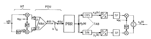
In the system outlined in Figure lb, a complex valued
analog baseband signal having the components x(t) and y(t)
is obtained in a Hilbert transformation stage from the real
value analog input signal. Compared to quadrature conversion
(Figure la), Hilbert transformation has the advantage of
being free from harmonics so that lowpass filters can be
omitted. Otherwise, however, the generation of the complex
baseband signals is of no further significance for the
present invention. The essential difference between the
system of Figure lb and the system sketched in Figure la is
1 335842
the phase-digital converter PDU which puts out the momentary
phases of the input signal with a resolution of N bits as a
quasi time-continuous digital phase signal ~(t). This
digital phase signal can be sampled at a very high clock
pulse rate k TA, i.e. at very short sampling intervals TA,
and can thus be converted into a time discrete succession of
digital phase words ~(k). The signal sequence ~(k) is fed to
signal processor PRR which emits, as its output signal, a
further succession of digital phase words ~p(k). These phase
words ~p(k) address a cosine and a sine memory table TAB so
that again a complex digital signal xR(k), yR(k) is available
which can be processed further in the same manner as the
complex signal wR(k), wI(k) of Figure la. Signal processor
PRR need process only a real signal sequence ~(k) and can
therefore be of simpler design or handle greater data rates
than if it were to process complex signals.
In principle, any A/D conversion can be described
completely in mathematical terms by integer divisions
z = int x~ (3)
with x representing the analog input value and z the output
word. The abbreviation "int" here represents the rounding or
break operator for the integral representation of code word
z. The divisor
~ = Ao 2-N (4)
-- 10 --
1 335842
which is identical with the resolution of the A/D converter,
is calculated from the control range Ao of the A/D converter
and the A/D converter word length N in bits.
This applies equally also for phase quantization. The
phase angles
~(t) = arc tan (t)
of a complex time signal
s(t) = x(t) + jy(t) = A(t) e j~(t) (6)
(or the complex conjugate signal
s*(t) = x(t) - jy(t) = A(t) e j~(t))
obtained, for example, with the aid of a Hilbert transforma-
tion (see Reference /l/) from a purely real-value time signal
s(t) (Figure lb), are quantized according to the basic
formula for digital phase angle values
~ = int arc tan ~
where the phase angle resolution should be set at
1 335842
e = 2~ . 2-N (N = binary digits in bits) (8)
Due to this "rounding off" of the phase angle according to
Equation (7), a remainder
~e = ~ - e ~ (g)
is left which cannot be represented and which describes the
systematic quantizing error of the phase quantizing process
and, in the ideal case, moves between the limits
lo e2 ' ~ e < + e2 (lo)
However, the technical conversion of the phase quantiza-
tion in this way is not always possible since in the case of
x = o in the argument of the arc tan function in Equation
(7) a division by zero will occur.
The principle of the method according to the invention
is shown in Figure 2.
In a signal phase generator SPG a set of signals is
generated which are each shifted relative to one another and
relative to the input signal, respectively, by the same
phase increments e (Equation (8)) and by the phase angle
ei = e (i - 1) (ll)
- 12 -
1 335842
These signals, hereinafter called signal phases and expressed
as follows
~i(t) = Re ~A (t) e~ e jei~ (12)
or as real/imaginary components:
~i(t) = ai x(t) + bi y(t) (13)
where i = 1, 2, 3, ..., n and n = 2N-l are generated as
indicated in Figure 2 by the phase shifters PSl to PSn of
signal phase generator SPG. Signal phase ~l(t) is assumed
not to have a phase shift relative to the input signal, i.e.
~i(t) = s(t). Signal phases ~i are applied to the inputs of
sign comparators VKl to VKn of a sign comparator bank VKB
which forms a set of Johnson sequences sqi(t) where i = 1, 2,
..., n from signal phases ~i according to the sgn (signum)
function. Signal phases ~l(t) to ~8(t) which are formed by
such a phase shift from a real input signal and the Johnson
sequences sql(t) to sq8(t) resulting therefrom are shown in
Figure 3. Johnson sequences are defined and described in
detail in reference /2/.
- 13 -
1 335~42
In the real case, the signal phases are not generated by
means of the phase shifting of a real input signal but by
parallel vector additions of the real and imaginary com-
-ponents of the complex input signal s(t) (Equation (6)).
In order to obtain a phase shift ei for the signal phase
~i(t), the phase coefficients ai and bi from Equation (13)
must meet the absolute condition
bi
_ = tan ei (14)
The rule expressed in Equation (14) is a significant feature
of the phase-digital conversion method according to the
invention and defines, in principle, the structure of signal
phase generator SPG as will be described in detail below.
Figure 4 depicts the development of signal phases ~i(t)
from the components of the complex input signal with the aid
of a vector diagram in the complex plane for the real
component x(t) and the imaginary component y(t) of signal
s(t). In an exemplary case, N = 4 has again been selected to
correspond to a phase angle resolution of 22.5. Starting
with the first signal phase ~1 which is not shifted in phase,
corresponding to el = 0, relative to the real input signal
and the real component x(t) of the complex signal, the
vectors of the phase shifted signal phases ~2~ ~3, ... to ~8
are each shifted clockwise by e = 22.5 in the lower half-
- 14 -
1 335842
space of the complex plane. This illustration also clearly
shows that no further signal phases are required to subdivide
the upper half-space and that it is merely necessAry to
invert signal phases ~1 to ~8. Also plotted in the diagram
S are changes in level of the associated sequences sqi(t) for
rotation at the phase of input signal ~(t) = w t. From the
diagram, by simple geometric considerations, the phase
coefficients ai, bi can also be derived by vector addition
from the components x(t), y(t) to form signal phases ~i.
The signs of the phase coefficients in the quadrants of the
complex plane are shown in Figure 5. The resulting Johnson
sequences sqi(t) are already shown in Figure 3.
The set of n binary Johnson sequences sqi(t) already
includes the momentary phase of the input signal in phase
quantized form and thus constitutes a time-continuous digital
signal. For the complete conversion into a form suitable for
digital signal processing, the phase quantization is followed
by phase value sampling at the sampling clock pulse k tA
and the sampling rate fA = l/TA. This digital sampling takes
place in parallel in a digital sequence sampler DSA which is
connected to the output of the sign comparator bank. The
~ampling is illustrated in Figure 2 by switches SAl to SAn
with subsequently connected clocked memory cells SPl to SPn
(clock pulse sequence TA). The digital sequence sampler may
1 335842
be realized very easily by fast D flip-flops or ~imilar
clocked memory cells. The sequence of the sampling values
sqi(k) obtained during parallel sampling form time discrete
sequences sqi(k). The values sqi(k) equal in time are the
momentary digital phase values of the input signal present in
the Johnson code. Advisably, a code converter ICU is
connected to the output of the digital sequence sampler to
convert the digital values which are present in the Johnson
code with 2N-l bit word lengths into a code better suitable
for further processing, for example the binary code or the
Gray code, with a word length of N bits and emits them as a
sequence of digital phase values ~(k).
Thus, the quar,tized phase value
sqll(t) = sq(l,T ) = sgn ~1(t)
s~2(t) = s~(2~T ) = sgn ~2(t)
~(t) = . . . . . . (15)
.
S~n(t) = s~(n,T ) = sgn ~n(t)
then results from the signal phases ~i(t) each mutually
shifted in phase by e and by application of the sign function
sgn as a set of n parallel Johnson sequences sq1 to sqn
(Figure 3), shifted in time by ~i which, according to the
- 16 -
1 335842
rule for a æingle sequence period, must here be fixed as
follows:
1 for ri < t < ri + Ts/2
8qli(t) = s~(i,Ts) = ~-1 for ri + TS/2 < t < ri + T~ (16)
lo for t < ri or t > ri + Ts
and for the individual sequence repetitions sq1(k) to sqn(k)
with
sgi(k) = sqli(t) ~T (t) = ) S~i ( T ) (17)
(where ~T(t) = Dirac surge rate at the equidistant spacing T,
T = sequence duration). The time shifts
i e Ts (i - 1) = Ts 2 N (i - 1) (18)
of the Johnson sequences sqi(t) and sqi(k), respectively,
thus correspond to the phase shifts of signal phases ~i(t)
having a period duration Ts by the angle e ( i - 1 ) .
Two particularly advantageous embodiments of phase-
digital converters (PDU) operating with a phase angle
resolution of 8 bits in the Johnson code or 4 bits in the
binary or Gray code (N = 4) for the realization of the phase-
digital conversion method (PDC) according to the describedbasic principle of Figures 2, 3 and 4 will now be described.
- 17 -
1 335842
They differ essentially in the structures of their signal
phase generators (SPG). The possibility of being able to
configure the SPG's as fully monolithically integrated
circuits in the conventional Si or GaAs technology is here a
particular advantage. This means that the individual
components of the SPG's themselves can be easily realized
primarily by active components, e.g. transistors, differen-
tial amplifiers, etc.
It is here always assumed that a complex input signal
s(t) is involved which is obtained from a real signal s(t) by
quadrature mixing or Hilbert transformation with a signal
e~jWMt and is present in the form of orthogonal signal com-
ponents x(t) and y(t) (Equation (6)). The generation of the
signal phases ~l(t) to ~8(t) takes place on the basis of
vector addition (Figures 4 and 5) from the orthogonal signal
components of the complex input signal.
The various embodiments of signal phase generators SPG
each meet the unrestricted condition of the phase coeffi-
cients ai and bi f Equation (14). This equation fixes only
the ratio of phase coefficient bi to phase coefficient ai and
thus permits other freely selectable subconditions for the
individual phase coefficients. This will be utilized in a
~pecial way in the examples to be described below.
- 18 -
1 335842
For technical use it is advisable to permit phase
coefficients ai and bi f Equation (13) to take on only
values which are less than 1 in amount. In the SPG this
-produces signal amplifications Ivl < 1 which can be realized
particularly easily by means of integratable, passive or
active components.
In the case of the first example according to Figure 6,
a subcondition which does not adversely affect the principle
of the method is assumed for the coefficients, namely:
¦ai¦ + ¦bi¦ = 1 (19)
From this result the equations for a determination of the
phase coefficients as follows:
15lail 1 + ¦tanei¦ and (20)
¦bi¦ = 1 - lai¦
The respective signs for ai and bi within the individual
quadrants of the phase quantization can here be found in
Figure 5.
According to these equations, the mathematical transfer
model - a purely parallel fanning open of the signal paths -
-- 19 --
1 335842
of such an SPG is shown in Figure 6 for P/D conversion with N= 4. The signal delays from complex signal mixing to the
individual signal summation points are here optimized, i.e.
the individual parallel signals each traverse only one
amplifier stage Vx and Vy~ respectively, with a gain of ¦Vi¦
S 1 (Vi = ai and bi, respectively).
The technical realization of the basic structure
sketched in Figure 6 takes advantage of the fact that the
sum formations ~i = aix + biy provided in Figure 6 can be
replaced by difference formations ~i = aixi ~ (-biY) = biY ~
(-aix) so that the summing members can be omitted and the
difference formation performed instead takes place immediate-
ly ahead of the sign comparators in that the signal com-
ponent (-aix) or (-biy), respectively, to be subtracted is
applied to the inverting input of the respective comparator.
The signal phases formed by vector addition will then not
appear explicitly but vector additions and sign formation of
the vector sums are then implied in the internal structure
of the comparators. Moreover, the phase-digital converter
according to Figure 7 utilizes the fact that instead of
weighting the signals with a negative coefficient, the
signals x(t) and y(t) are advantageously conducted through
amplifiers VP which have an additional inverting output and
the inverted signal components are weighted with a positive
- 20 -
1 335842
coefficient. Weighting of the signals takes place in
amplifier elements Vx and Vy~ respectively, whose amplifica-
tion factors are shown i~ Figure 7.
In deviation from Figure 6, the coefficients resulting
from Equation (20) are not taken over; instead the arrange-
ment is designed in such a manner that only two amplification
factors of different amounts occur. The condition of
Equation (14) is of course also met in this embodiment. In
order to uniformly load all outputs of amplifiers VP, a
19 buffer amplifier P having a negative coefficient is addition-
ally provided which, if such uniform loads are not desired,
could also be connected with a positive coefficient to the
other output of the signal amplifier. Further embodiments
which vary in details, particularly in weighting factors and
combination, are also conceivable.
Digital sampling of Johnson sequences sql to sq8
available at the outputs of comparators VK is then advantage-
ously done with the aid of D-flipflops DF actuated by the
sampling clock pulse signal k-TA. The phase values available
in a Johnson Code having a width of 8 bits are converted in a
Johnson code converter JCK into, for example, the 4-bit Gray
code.
In the case of the second example shown in Figures 8, 9
and 10, the signal phase generator (SPG) is realized in a
- 21 -
1 335~42
different way, with of course the condition for the phase
coefficients (Equation 14) being again fully met.
A significant difference compared to the basic structure
of the signal phase generator sketched in Figure 6 is the
stepwise halving of the quantization phase angle by vector
addition of the available signal phases into new signal
phases having different phase delays. Starting with the
orthogonal components x(t) and y(t) which can be considered
to be signal phases of a first quantization stage having a
phase angle resolution of ~/2, new signal phases are formed
by vector addition and their phase delays cut the phase angle
resolution in half to ~/4. The procedure continues in this
way until the desired phase angle resolution has been
attained. Figure 8 shows the basic principle.
For a desired phase angle resolution of e = 2~ 2-N,
the invention provides that 2N-1 signal phases ~i(t) are to
be formed. If ~i(t) is set to equal x(t), the further
signal phase for N = 4 directly results as ~5(t) = -y(t).
These two signal phases produce a quadrant division of the
complex plane corresponding to a phase angle resolution of
~/2. By vector addition in a subsequent step, further signal
phases ~(t) = ~l(t) + ~s(t) = x(t) - y(t) and -~t = ~l(t) -
~5(t) = x(t) + y(t) are generated with which the complex
plane is subdivided further into angle increments ~/4 and
- 22 -
1 335842
thus the previo~s phase angle resolution is cut in half.
While generally the orthogonal signal component x(t) and
y(t) and signal phases ~l(t) and ~2(t), respectively, are
-identical in amplitude, the signal phases ~3 and ~t have an
amplitude which is higher by ~. Therefore, before the phase
angle resolution is halved further in basically the same
manner, the signal phases are st~n~Ardized to the same
amplitude in that ~3 and ~t are weighted with a factor
Cl 2cos(~/4) 0.71
and are thus reduced in amplitude to the standardized signal
phases ~3 and ~7. From the now available signal phases ~1
~3, ~5 and ~7, vector addition produces new signal phases
~2 = ~1 + ~3, ~4 = ~3 + ~5, etc. which further halve the
phase angle resolution to ~/8 and are entered in the vector
diagram of Figure 8. Thus all signal phases required for the
desired phase angle resolution with N = 4 are available.
Since only the signs of the signal phases are evaluated, the
last signal phases formed, i.e. ~2~ ~4, ~ and ~8, need not
be standardized in amplitude. Only for the case that the
phase angle resolution is to be further cut in half in an
additional step, these signal phases are standardized in
amplitude by weighting them with a scaling factor
- 23 -
~ 335842
C2 = 2cos(~/8)
Thus, a binary tree structure as sketched in Figure 9
results for the structure of a signal phase generator
operating according to the described principle of successive
halving of the phase angle resolution. The orthogonal signal
components x(t) and y(t) are generated in the manner already
described. Summing members (~) are shown which consider the
signs for vector addition and scaling factors Cl and C2 for
amplitude standardization. Since, as explained, scalings
with C2 are not required if the phase angle resolution is
limited to that realized with ~1 to ~8~ a tree structure
results which is able to operate with a minimum of weighting
1~ coefficients. However, compared to the parallel fan struc-
ture (Figure 6), this tree structure cannot be realized with
a minimum of delay.
The same considerations as made for the phase-digital
converter shown in Figures 6 and 7 can be utilized here for
the technical realization of a phase-digital converter. In
the structure of such a phase-digital converter shown in
Figure 10, inverted signals are additionally generated in
amplifiers VP from the orthogonal input signal components
x(t) and y(t). The signal phases ~l(t) and ~5(t) are applied
1 335842
directly to the inputs of the associated ~ign comparators.
The vector additions including standardization to obtain the
signal phases ~3(t) and ~7(t) are performed by means of
-differential amplifiers VD having their amplification factor
set at V = Cl. The remaining vector additions for ~2~ ~4~ ~6
and ~8 together with the sign formation are moved, in the
manner described in connection with Figure 7, to comparators
K. The further processing with sampling and code conversion,
here to the 4-bit binary code, takes place analogously to the
phase-digital converter of Figure 7.
It will be understood that the above description of the
present invention is susceptible to various modifications,
changes and adaptations, and the same are intended to be
comprehended within the meaning and range of equivalents of
the appended claims.
1 335842
BIBLIOGRAPHY
/1/ H. D. Luke, Signalubertragung [Signal Transmission],
published by Springer Verlag, Third Edition, Berlin,
Heidelberg, New York, Tokyo, 1985.
/2/ X. G. Beauchamp, Applications of Walsh and Related
Functions with an Introduction to Sequency Theory,
Academic Press, London, Orlando, San Diego, New York,
Toronto, Montreal, Sidney, Tokyo, 1984.
/3/ G. Webber, J. Culp, M. Robinson, DRFM Requirements
Demand Innovative Technology, Microwave Journal,
February, 1986, pages 91-104.
- 26 -