Note: Descriptions are shown in the official language in which they were submitted.
1337211
FLUORESCENT LAMP CONTROLLERS
This invention relates to fluorescent lamp
controllers and more particularly to controllers for
operating fluorescent lamp or other loads at high
efficiency while being very safe and highly reliable in
operation and readily controllable and while achieving a
long lamp life. The controllers of the invention are
adaptable for use with different types and sizes of
fluorescent lamps or with other loads and are readily and
economically manufacturable.
It is well known that fluorescent lamps are more
efficient when operated at higher frequencies. As a result
of this fact and also as a result of continuing
improvements in SMPS (Switch Mode Power Supply) circuits
and components, there have been ~any proposals for using
SMPS circuits operable at high frequencies for energizing
and controlling fluorescent lamps. A relatively early
disclosure is contained in the Wallace U. S. Patent No.
3,611,021, issued October 5, 1971. In the circuit as
disclosed in the Wallace patent, a fluorescent lamp is
connected in series with a capacitor to the secondary
winding of a transformer which has a primary winding
connected to a pair ~f switching transistors which
alternately conduct to apply a square wave current to the
primary winding and which are driven by a saturable core
oscillator the frequency of which is controlled in response
to a current sense signal at the output. The secondary
winding, the lamp and a capacitor are in series and form a
-- 1337211
.
tuned circuit which has a resonant frequency which is
determined by the leakage inductance of the transformer and
by the series capacitor. For starting, a second capacitor
is connected in parallel with the secondary winding and the
series combination of the first capacitor and the lamp, the
.
second capacitor having a value such as to be resonant at a
harmonic of the operatin~ ~requency.
The Stolz U. S. Patent No. 4,251,752 discloses a
circuit in which an inverter circuit having a constant
frequency of operation is connected to a fluorescent lamp
load and is supplied with a DC operating voltage developed
across a capacitor by a variable duty cycle converter
circuit which is connected to the output of a rectifier
circuit. A loop amplifier circuit is shown having one
input connected to a ramp circuit and a second input
connected to the output of the rectifier circuit to be
responsive to both rectifier current and voltage, the loop
amplifier circuit being described as being operative to
control the duty cycle of the converter circuit to maintain
the input current to the rectifier in phase with the input
voltage.
Additional disclosures relating to the use of
SMPS circuits are contained in the Stupp et al. U. S.
Patent No.s 4,453,109, 4,498,031, 4,585,974, 4,698,554 and
4,700,113. Patent No. 4,453,109 discloses a high frequency
oscillator-inverter with a novel leakage reactance
transformer which provides not only the current limiting
ballast function but also automatic control of heater
power. Patent No. 4,498,031 discloses a non-resonant
coupling network which includes a reactive ballast
impedance coupled between a lamp and the output of a
trapezoidal waveform generator, with frequency being
altered as a function of lamp current. Patent No.
4,585,974 and Patent No. 4,698,554 disclose driven
~ _3- 1337211
inverters which are coupled to a lamp through non-resonant
networks which include reactive ballast impedances, the
frequency of the inverter as disclosed in each patent being
controlled on a cycle-by-cycle basis as a function of the
amplitude of lamp current. Patent No. 4,700,113 discloses
a circuit in which a high frequency inverter is coupled to
a-lamp through a reactive ballast l`~pe~a~Ce, the inverter
being operated at a predetermined frequency until ignition
occurs and its frequency being then automatically increased
to a desired operating frequency.
- The Zeiler U. S. Patent No. 4,717,863 discloses
a circuit which is similar to those of the Wallace and
Stupp et al. patents in that frequency is controlled to
control the output. Lamps are connected to the secondary
winding of transformer and an inductor separate from the
transformer is connected in series with a capacitor and a
primary winding of the transformer to obtain an output
which increases as the frequency is reduced, frequency
being controlled by a photocell arrangement responsive to
light output.
There are many other prior art disclosures of
the use of SMPS circuits for energizing fluorescent lamp
loads. Many of the prior art circuits and particularly
those disclosed in the Stupp et al. patents have been very
successful. However, for the most part, the SMPS circuits
as proposed in the prior art have been such that they would
be unduly expensive to manufacture and/or would have severe ~
limitations with respect to performance and reliability and
have not enjoyed substantial commercial success.
This invention was evolved with the general
object of providing fluorescent lamp controllers which have
4 1337211
a very high efficiency and which achieve a long lamp life
while being extremely safe and reliable in operation and
also being readily controllable. It is also an object of
the invention to achieve such goals with controllers which
are easily adaptable for use with different types and sizes
of fluorescent lamps and which are readily and economically
manufacturable~
Controllers constructed in accordance with the
invention are similar to those disclosed in the
aforementioned Stupp et al. patents in that a fluorescent
lamp load is coupled to the output of a variable frequency
DC-AC converter or inverter. A half-bridge circuit is used
in an illustrated embodiment and it is supplied with a
variable frequency gating signal which is controllable in
response to lamp current to obtain a substantially constant
lamp current.
Important features of the invention relate to
the construction and mode of operation of an output circuit
which couples the output of the variable frequency DC-AC
converter circuit to the fluorescent lamp load. In the
disclosed embodiment, an output circuit includes a resonant
circuit and it is similar to that disclosed in the
aforementioned Wallace patent in that it operates at a
frequency above resonance and also in that it includes a
resonant capacitor which is connected in circuit with the
secondary winding of a transformer and the load, the
resonant frequency being determined by the values of the
leakage inductance of the transformer and the value of the
capacitor. However, the construction of the output circuit
and the control of its operation, through control of the
variable freg~ency DC-AC converter, are quite different
from those disclosed by the Wallace patent, particularly
with respect to connections and characteristics of circuit
components and control of starting operations and
~5~ 1337211
operations after.starting, providing a number of important
advantages.
In a controller of the invention, the output
circuit operates as a tuned circuit having characteristics
such that a voltage is produced which is sufficient for
ignition at a frequency which is offset in one direction
from a-resonant frequency. The tuned circuit has
characteristics such that the frequency may then be
controlled after ignition in a range offset in the same
direction from a resonant frequency to control lamp output.
A control circuit is provided for automatically operating
upon energization of the controller for operating the DC-AC
converter at a certain high frequency, above that at which
ignition would normally occur, and then gradually reducing
the frequency until ignition occurs, the control circuit
being then operative to control the lamp current through
control of the frequency of operation of the DC-AC
converter.
Preferably, the resonant frequency is below the
ignition and operating frequencies and a specific feature
relates to the provision of an arrangement such that the
resonant frequency is reduced in response to the increased
load which occurs upon lamp ignition, operative in a manner
such as to insure operation at a frequency above resonance
and to obtain a high degree of reliability. Preferably a
transformer is used of a type.similar to that disclosed in
the aforementioned Stupp et al. Patent No. 4,453,109. It
is found that the use of such a transformer facilitates the ~
automatic reduction in the resonant frequency as a function
of load.
The use of the arrangement including such a
transformer has an additional important advantage in that
such a transformer is operable to automatically control
~ -6- 1337211
magnetic coupling between a-primary winding and filament
windings. A tighter magnetic coupling to the filament
windings is obtained during a pre-heat phase of operation
in which the load is very light and the ignition phase is
then initiated. Upon ignition to enter an operating phase,
the transformer is such as to respond to the increased load
and automatically reduce the magnetic coup~ing to the
filament windings and lower the filament voitage. The
arrangement thus operates to prevent damage to and to
extend the life of-the filaments.
Another specific feature of the output circuit
relates to the connection-of the resonant capacitor in
parallel relation to the fluorescent lamp load and the
transformer winding so as to limit the voltage across the
winding in accordance with lamp voltage. The parallel
arrangement also facilitates the use of a single resonant
capacitor for both the ignition and operating phases.
With the aforementioned features, stable
operation in a range well above the resonant frequency is
facilitated, which has a very important advantage in
insuring that transistors of the DC-AC converter are
protected against a capacitive load condition, i.e., one in
which the current leads the voltage and in which
destruction of the transistors might result. A further
feature relates to the provision of additional protection
through the use of circuitry which automatically switch to
a safe condition when the phase of current relative to
voltage is less than a certain safe value, preferably by
sweeping the DC-AC converter to a high frequency.
Additional features of the invention relate to
the provision of a pre-conditioner circuit which is
supplied with a full-wave rectified 50 or 60 Hz voltage and
which includes SMPS circuitry operating as an up-converter
- 1337211
to supply a DC voltage to the DC-AC converter which is
automatically maintained at a relatively high level for
stable efficient operation. The automatic level control is
obtained by controlling the width of gating pulses applied
to the circuit in response to a signal which is
proportional to the average value of the output voltage of
the pre-conditioner circuit.
- A specific feature is that the pulse width is
also controlled in response to a second signal which is
proportional to the instantaneous input signal to the pre-
conditioner circuit, in a manner such as to obtain power
factor control while also obtaining the aforementioned ! j - '
automatic level control. Preferably, the sum of an ,
inversion of the second signal and a constant are
multiplied by the first signal which is proportional to the
average output voltage, to obtain a signal for control of
pulse width. It is also preferable that the circuit be
operated in a discontinuous mode. It is found that
excellent results are obtained, both with respect to
obtaining the desired current waveform and with respect to
obtaining a substantially constant output level, by
combining only the two signals in this manner. The
invention avoids instability problems from a feedback loop
which results when a signal corresponding to input current
is used in controlling pulse width.
A number of very important additional features
of the invention relate to the construction and operation
of a control circuit which controls both the DC-AC
converter and the pre-conditioner circuit. The control
circuit is preferably implemented as a single integrated
circuit component or "chip" arranged for use with external
components in a manner such as to be usable with different
types of fluorescent lamp or other loads of similar nature
and to permit selection of external component values to
-8- 1337211
obtain optimum performance with any particular type of
fluorescent lamp or other load connected thereto.
Controllers which are constructed in accordance with the
invention are particularly advantageous for energization of
fluorescent lamps, halogen lamps or other gaseous discharge
devices as well as for energization of other types of loads
and i~ will be understood that fluorescent lamp loads are
referred to herein for ease of description and that
reference herein and in-the claims to fluorescent lamps and
fluorescent lamp loads are to be construed as including all
other types of loads capable of being energized by the
controllers.- It will also be understood that the various
features of the invention are not limited to implementation
of the control circuit through the use of a single
integrated circuit.
An important aspect of the invention relates to
the discovery and recognition of the sources of reliability
problems which resulted when attempting to use cascaded
pre-conditioner and DC-AC converter circuits. It was found
that with both operating at high frequencies and in close
proximity, the signals may be transmitted from each circuit
to the other to interfere with proper operation and, in
some cases, to cause malfunctions such as to produce
complete breakdowns. In accordance with the invention, the
operations of the two circuits are synchronized and are
either in the same phase or have a fixed or controlled
phase relation to one another, preferably with both
operated at the same frequency. In an illustrated
embodiment, an oscillator circuit which supplies a square
wave signal to the DC-AC converter operates during each
cycle of the square wave signal to produce a control signal
to a pulse width modulator circuit to control the
initiation of a pulse of variable width, the pulse width
modulator being used to supply the gating pulses which are
required for operation of the pre-conditioner circuit.
1337211
g 20104-8557
Further features relate to start up operations after
initial energization of the controller and to a number of safety
and protection features which insure a high degree of reliability
and protect against destructive failures which might otherwise
result from use of defective lamps or the absence of lamps or from
any one of many possible problems. The control circuit initially
obtains power from the input rectifier circuit and subsequently
from the DC-AC converter, after applying the required gating
signals to the pre-conditioner and converter circuits. The
aforementioned pre-heat phase is initiated for heating of the lamp
filaments, followed by the aforementioned ignition and operating
phases. If ignition is not initially obtained, one or more repeat
attempts are made until ignition is successfully obtained.
Safeties are automatically effected in response to excessive lamp
voltage or currents, and excessive or insufficient voltages or
currents at key points in the circuit and, as aforementioned, in
response to unsafe voltage-current phase relations in the DC-AC
converter circuit.
In summary, according to one broad aspect, the present
invention provides a controller for a fluorescent lamp load,
comprising: DC-AC converter means having an input and an output,
DC supply means coupled to said input, output circuit means
coupled to said output and arranged for coupling to-said
fluorescent lamp load, and control means for controlling operation
of said DC-AC converter and said DC supply means, said output
circuit means including inductance means and resonant capacitor
means forming a circuit which is resonant at no-load and load-
condition resonant frequencies with loads equivalent to those
..... .
9a 1337211 20lo4_8557
respectively obtalned prlor to and after lamp lgnltlon, sald
control means belng arranged to operate in a lamp ignition phase
to operate sald converter at a frequency within a range above said
no-load resonant frequency, and said control means being arranged
to operate in an operating phase after lamp ignition to operate
said converter in a frequency range above said load-condition
resonant frequency, said control means comprising means to effect
a change in the frequency of operation of said inductance means
from a condition prior to lamp ignition to a substantially
different condition after lamp ignition such that said load-
condltlon resonant frequency ls substantially lower than said no-
load resonant frequency.
According to another broad aspect, the present invention
provides a controller for a fluorescent lamp load, comprising: DC-
AC converter means having an input and an output, DC supply means
coupled to said input, output circuit means coupled to said output
and arranged for coupllng to sald fluorescent lamp load, and
control means for controlllng operation of said converter and
supply means, said DC supply means comprising input rectifier
means arranged to develop a full-wave rectified AC voltage, and a
first switch mode power supply circuit having a gating pulse input
and arranged to convert said rectifled AC voltage to a DC output
voltage havlng a magnitude controlled by the wldth of hlgh
frequency gating pulses applied to said gating pulse input, and
said DC-AC converter means comprising a second switch mode power
supply for developing an AC output controlled by gating pulses
applied thereto, said control means including first pulse supply
means for applying a first high frequency gating pulse signal to
1337211
9b 20104-8557
sald flrst swltch mode power supply clrcult and second pulse
supply means for applylng a second hlgh frequency gatlng pulse
signal to said second swltch mode power supply, said first and
second gating pulse signals being applied in synchronlzed relation
to each other, wherein sald output clrcuit means lncludes
lnductance means and resonant capacltor means, sald control means
belng arranged to slmultaneously vary the frequency of both of
said flrst and second gatlng pulse signals applied from said first
and second pulse supply means to said first and second switch mode
power supply means.
According to yet another broad aspect, the present
invention provides a controller for a fluorescent lamp load,
comprising: DC-AC converter means having an input and an output,
DC supply means coupled to said input, output circuit means
coupled to said output and arranged for coupling to said
fluorescent lamp load, and control means for controlling operation
of said converter and supply means, said DC-AC converter means
comprising a switch mode power supply circuit which includes
transistor means, and said output circuit means including
inductance and capacitance means and being operative under normal
operation and load conditions to present an inductive load to said
switch mode power supply such that currents through said
transistor means lagging phase relation to applied voltages, and
protection means for developing and comparing signals which
correspond to said currents through said transistor means and said
applied voltages to measure the phase of currents through sald
transistor means relative to said applied voltage, and means for
gc 1 3 3 7 2 1 1 2ol04-8557
effecting a predetermlned change in the frequency of operation of
said
1337211
gd 20104-8557
converter means in response to a shift of said measured phase in a
leading direction and beyond a certain threshold phase.
According to still another broad aspect, the present
invention provides a controller for a fluorescent lamp load
comprising: DC-AC converter means including a switch mode power
supply circuit and having an input and an output, DC supply means
coupled to said input, output circuit means coupled to said output
and arranged for coupling to said fluorescent lamp load, and
control means for controlling operation of said converter and
supply means, said DC supply means comprising input rectifier
means arranged to develop a full-wave rectified AC voltage, and a
switch mode power supply circuit having a gating pulse input and
arranged to convert said rectified AC voltage to a DC output
voltage having a magnitude controlled by the width of high
frequency gating pulses applied to said gating pulse input,
voltage supply means for said control means, a supply voltage
being applied to said voltage supply means from said input
rectifier means at least during a starting time interval following
application of an input AC voltage to said input rectifier means,
wherein said control means comprises means for inhibiting
operation of said switch mode power supply circuits until after
said supply voltage has reached a certain trip point.
This invention contemplates other objects, features and
advantages which will become more fully apparent from the
following detailed description taken in conjunction with the
accompanying drawings.
FIGURE 1 is a schematic diagram illustrating a
fluorescent lamp controller which is constructed in accordance
1337211
9~ 20104-8557
with the invention;
FIGURE 2 is a circuit diagram of an output circuit of
the controller of FIG. 1;
A ~ ;
- -lo- 1337211
FIGURE 3 is a graph illustrating characteristics
of the output circuit and its mode of operation;
FIGURE 4 is a circuit diagram of a DC-AC
converter circuit of the controller of FIG. l;
FIGURE 5 is a circuit diagram of a pre-
conditioner circuit of the controller of FIG. l;
FIGURE 6 is a circuit diagram of an input
rectifier circuit of the controller of FIG. l;
FIGURE 7 is a circuit diagram of a voltage
supply circuit of the controller of FIG. 1;
FIGURE 8 is a schematic diagram of a portion of
logic and analog circuitry incorporated in a control
circuit of the controller of FIG. 1 and operative for
generating high frequency square wave and pulse-width
modulated gating signals;
FIGURE 9 is a schematic diagram of another
portion of logic and analog circuitry incorporated in a
control circuit of the controller of FIG. 1 and operative
for developing a frequency control signal;
FIGURE 10 is a schematic diagram of a third
portion of logic and analog circuitry incorporated in a
control circuit of the controller of FIG. 1 and operative
for developing various control signals; and
FIGURE 11 is a graph illustrating the waveforms
produced in phase comparison circuitry shown in FIG. 9, for
explanation of the operation thereof.
133 7211
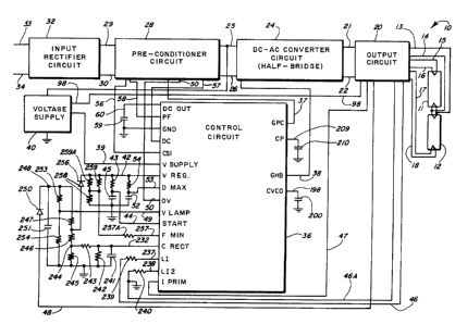
Reference numeral 10 generally designates a
fluorescent lamp controller constructed in accordance with
the principles of this invention. As shown in Figure 1,
two lamps 11 and 12 are connectable through wires 13-18 to
an output circuit 20, wires 13 and 14 being connected to
one filament electrode of lamp 11 and one filament
electrode of lamp 12, wires 15 and 16 being connected to
the other filament electrode of lamp 11 and wires 17 and 18
being connected to the other filament electrode of lamp 12.
It will be understood that the invention is not limited to
a controller for use with two lamps only.
The output circuit 20 is connected through lines
21 and 22 to the AC output of a DC-AC converter circuit 24
which is connected through lines 25 and 26 to the output of
a pre-conditioner circuit 28, the circuit 28 being
connected through lines 29 and 30 to the output of input
rectifier circuit 32 which is connected through lines 33
and 34 to a source of a 50 or 60 Hz, 120 volt RMS voltage.
In the operation of the illustrated embodiment, the pre-
conditioner circuit 28 responds to a full-wave rectified 50
or 60 Hz voltage having a peak value of 170 volts,
developed at the output of circuit 32 to supply to the DC-
AC converter circuit 24 a DC voltage having an average
magnitude of about 245 volts. The DC-AC converter circuit
24 converts the DC voltage from the pre-conditioner circuit
28 to a square wave AC voltage which is applied to the
output circuit 20 and which has a frequency in a range of
from about 25 to 50 KHz. It will be understood that values
of voltages, currents, frequencies and other variables, and
also ~he values and types of various components, are given
by way of illustrative example to facilitate understanding
of the invention, and are not to be construed as
limitations.
-12- 1337211
Both the pre-conditioner circuit 28 and the DC-
AC converter circuit 24 include SMPS (switch mode power
supply) circuitry and they are controlled by a control
circuit 36 which responds to various signals developed by
the output circuit 20 and-the pre-conditioner circuit 28.
In ~he .llustrated controller 10, the pre-conditioner
circui~ 28 is a variable duty cycle up-converter and is
supplied with a pulse-width modulated gating signal "GPC"
which is applied through line 37 from the control circuit
36. The DC-AC converter circuit 24 is a half-bridge
converter circuit in the illustrated controller 10 and is
supplied with a square wave gating signal "GHB" which is
applied through a line 38 from the control circuit 36. In
accordance with an important feature of the invention, such
gating signals are synchronized and may be phase shifted to
avoid interference problems and to obtain highly reliable
operation. In the illustrated preferred embodiment, they
are developed at the same frequency.
The control circuit 36 is an integrated circuit
in the illustrated embodiment and it includes logic and
analog circuitry which is shown in Figures 8, 9 and 10 and
which is arranged to respond to various signals applied
from the pre-conditioner and output circuits 28 and 20 to
develop and control the "GPC" and "GHB" signals on lines 37
and 38. Certain external components and interface
circuitry which are shown in Figure 1 are also shown in
Figure 9 and are described hereinafter in connection with
Figure 9.
Upon initial energization of the controller and
during operation thereof, an operating voltage is supplied
to the control circuit 36 through a "VSUPPLY" line 39 from
a voltage supply 40. A voltage regulator circuit within
the control circuit 36 then develops a regulated voltage on
- -13- 1337211
a "VREG" line 42 which is connected to various circuits as
shown.
,
- As shown, the "VREG" line 42 is connected
through a resistor 43 to a "START" line 44 which is
connected through a capacitor 45 to circuit ground.
Following energ ~ation of the controller 10, a voltage is
developed on the "START" line 44 which increases as a
exponential function of time and which is used for control
of starting operations as hereinafter described in detail.
In a typical operation, there is a pre-heat phase in which
high frequency currents are applied to the filament
electrodes of the lamps 11 and 12 without applying lamp
voltages of sufficient magnitude to ignite the lamps. The
pre-heat phase is followed by an ignition phase in which
the lamp voltages are increased gradually toward a high
value until the lamps ignite, the lamp voltages being then
dropped in response to the increased load which results
from conduction of the lamps.
Important features relate to the control of lamp
voltages through control of the frequency of operation,
using components in the output circuit 20 to obtain
resonance and using a range of operating frequencies which
is offset from resonance. In the illustrated embodiment,
the operating range is above resonance and a voltage is
developed which increases as the frequency is decreased.
For example, during the pre-heat phase, the frequency may
be on the order of 50 KHz and, in the ignition phase, may
then be gradually reduced toward a resonant frequency of 36
KHz, ignition being ordinarily obtained before the
frequency is reduced to below 40 KHz.
Upon ignition and as a result of current flow
through the lamps, the resonant frequency is reduced from a
higher no-load resonant frequency of 36 KHz to a lower
-14- 1337211
load-condition resonant frequency close to 20 KHz. The
operating frequency is in a relatively narrow range around
30 KHz, above the load-condition resonant frequency. It is
controlled in response to a lamp current signal which is
5 developed within the output circuit 20 and which is applied
to the control circuit 3~ t~r~gh current sense lines 46
and 46A, the line-46A being a ground reference line. When
the lamp current is decreased in response to changes in
operating conditions, the frequency is reduced toward the
lower load-condition resonant frequency to increase the
output voltage and oppose the decrease in lamp current.
Similarly, the frequency is increased in response to an
increase in lamp current to decrease the output voltage and
oppose the increase in lamp current.
As hereinafter described, the use of an
operating frequency which is above the load-condition
resonant frequency has an important advantage in providing
a capacitive load protection feature, operative to protect
against a capacitive load condition which might cause
destructive failure of transistors in the DC-AC converter
circuit 24. Additional protection is obtained through the
provision of circuitry within the output circuit 20 which
develops a signal on a "IPRIM" line 47 which corresponds to
the current in a primary winding of a transformer of the
circuit 20 and which is applied to the control circuit 36.
When the phase of the signal on line 47 is changed beyond a
safe condition, circuitry within the circuit 36 operates to
increase the frequency of gating signals on the "GHB" line
38 to a safe value, to provide additional protection of
transistors of the DC-AC converter circuit 24.
During the pre-heat and ignition phases of
operation, and also in response to lamp removal, a lamp
voltage regulator circuit limits the maximum open circuit
voltage across the lamps, operating in response to a signal
1337211
applied through a voltage sense line 48 and to a "VLAMP" input
line or terminal 49 of the control circult 36, through
lnterface clrcultry whlch ls shown ln Flgure 1 and also ln
Flgure 9 and whlch ls descrlbed herelnafter ln connectlon wlth
Figure 9. The lamp voltage regulator circuit operates to
effect a re-ignltlon operatlon ln whlch the operating frequen-
cy is rapldly swltched to lts maxlmum value and then gradually
reduced from its maximum value to lncrease the operatlng
voltage, to thereby make another attempt at ignltlon of the
lamps.
The lamp lgnltion and re-lgnltlon operatlon is also
effected ln response to a drop in the output voltage of the
pre-conditloner clrcult 28 below a certaln value, through a
comparator wlthin clrcult 36 which ls connected through an
"OV" llne 50 to a voltage-dlvlder clrcult wlthin the pre-
conditloner clrcuit 28, the voltage on the "OV" line 50 being
proportional to the output voltage of the pre-conditloner
circuit 28 to prevent operation at a low pre-conditioner
voltage.
The deslgnatlon of llne 50 as an "OV" line has
reference to its connectlon to another comparator wlthln
clrcult 36 whlch responds to an over voltage on the llne 50 to
shut down operatlon of the pre-condltloner clrcuit 28.
Another important protective feature of the control-
ler relates to the provision of low supply lock-out protection
clrcuitry, operative to compare the voltage on the "VSUPPLY"
line 39 with the "VREG" voltage on line 42 and to prevent
20104-8557
15a 1337211
operatlon of the pre-condltloner clrcult 28 and the DC-AC
converter circuit 24 until after the voltage on line 39 rises
above an upper trlp-polnt. After clrcults 28 and 24 are
operatlve, the same circultry operates to dlsable the clrcults
28 and 24 when the voltage on line 39 drops below a lower
trip-polnt. Then the DC-AC converter
20104-8557
-16- 1337211
circuit 24 is not allowed to be enabled until after the
voltage on line 39 exceeds the upper trip point and a
minimum time delay has been exceeded. The required time
delay is determined by the values of a capacitor 52 which
S is connected between a "DMAX" line 53 and ground and a
resistor 54 connected between line 53 and the "VREG" line
42.
-
- Another feature of the controller 10 relates to
the provision of an overcurrent comparator within circuit
36 which is connected through a "CS1" line 56 to the pre-
conditioner circuit 28 and which operates to disable
application of gating signals from the "GPC" line 37 to the
pre-conditioner circuit 28 when the current to the circuit
28 exceeds a certain value.
Additional features relate to the control of the
duration of the gating signals applied from the "GPC" line
37 to the pre-conditioner circuit 28 to maintain the output
voltage of the pre-conditioner circuit 28 at a
substantially constant average value while also controlling
the durations of the gating signals in a manner such as to
minimize harmonic components in the input current and to
obtain what may be characterized as power factor control.
In implementing such operations, the control circuit 36 is
supplied with a DC voltage on a "DC" line 57 which is
proportional to the average value of the output voltage of
the pre-conditioner circuit 28. Circuit 36 is also
supplied with a voltage on a "PF" line 58 which is
proportional to the instantaneous value of the input
voltage to the pre-conditioner circuit 28. An external
capacitor 59 is connected to the circuit 36 through a
"DCOUT" line 60 and its value has an advantageous effect on
the timing of the gating signals. It is also important for
loop compensation of the pre-conditioner control circuit
28.
1337211
17
As shown in Flgure 2, the output clrcult 20
comprlses a transformer 64 whlch ls preferably constructed ln
accordance wlth the teachlngs ln the Stupp et al. U.S. Patent
No. 4,453,109. As dlagrammatlcally lllustrated, the trans-
former 64 comprises a core structure 66 of magnetlc materlal
whlch lncludes a sectlon 67 on whlch a prlmary wlndlng 68 ls
wound and a sectlon 69 on whlch secondary wlndlngs 70-74 are
wound, sectlons 67 and 69 havlng ends 67A and 69A adiacent to
each other but separated by an alr gap 75 and havlng opposlte
ends 67B and 69B lnterconnected by a low-reluctance sectlon 76
of the core structure 66. In addltlon, although not used ln a
preferred embodlment, the core structure may optlonally
lnclude a sectlon 77 as lllustrated, extendlng from the end
69A of the sectlon 69 to a polnt whlch ls separated by an alr
gap 78 from an lntermedlate polnt of the sectlon 77. After
lgnltlon, a relatively hlgh current flowing ln the secondary
wlndlngs 70-74 produces a condltlon ln whlch the resonant
frequency ls reduced and the "Q" ls also reduced.
Secondary wlndlngs 70, 71 and 73 are fllament
wlndlngs coupled to the heater electrodes through capacltors
whlch protect agalnst shortlng of fllament wlres. Wlndlng 72
ls the lamp voltage supply wlndlng and windlng 74 supplies the
lamp voltage signal on llne 48. As shown, one end of windlng
70 ls connected through a capacltor 79 to the wlre 13, the
other end being directly connected to wlre 14. One end of
wlndlng 71 ls connected through a capacltor 80 to the wire 15
whlle the other end ls dlrectly connected to the wlre 16. One
20104-8557
17a 133~
end of wlnding 73 is connected to the wlre 17 through a
primary windlng 81 of a current transformer 82 whlle the other
end of windlng
20104-8557
-18- 1337211
73 is connected to the wire 18 through a capacitor 83 and
through a second primary winding 84 of current transformer
82. One end of winding 72 is connected to wire 16 while
the opposite e,nd thereof is connected through a capacitor
86 to a junction point which is connected through a
capacitor 87 to the wire 16, through a capacitor 88 to the
wire 14 and throug~ the winding 81 to the wire 17. The
current transformer 82 has a secondary winding 90 which is
connected in parallel with a resistor 91 and to the current
sense lines 46 and 46A.
,~ One end of the primary winding 68 is connected
,through a coupling capacitor 93 to the input line 21 while
the ,other end thereof is connected through a current sense
resistor 94 to the other input line 22 which is connected
to circuit ground. Coupling capacitor 93 operates to
remove the DC component of a square wave voltage which is
applied from the DC-AC converter circuit 24. The "IPRIM"
line 47 is connected through a capacitor 95 to ground and
through a resistor 96 to the ungrounded end of the current
sense resistor 94. A tap on the primary winding 68 is `-
connected through a line 98 to the voltage supply 40, to
supply a square wave voltage of about + 20 volts for
operation of the voltage supply 40 after a start operation
as hereinafter described.
The output circuit operates as a resonant
circuit, having a frequency determined by the effective
leakage inductance and the secondary winding inductance and
the value of capacitor 87 which operates as a resonant
capacitor. Capacitor 87 is connected across the series
combin~tion of t~e two lamps 11 and 12 and is also
connected across the secondary winding 72 through the
capacitor 86 which has a capacitance which is relatively
high as compared to that of the resonant capacitor 87 and
which operates as a anti-rectification capacitor.
-lg- 1337211
Capacitor 88 is a bypass capacitor to aid in starting the
lamps and has a relatively low value.
The graph of Figure 3 shows the general type of
operation obtained with an output circuit 20 such as
illustrated. Dashed line 100 indicates a no-load response
curve, showing the voltage which might theoretically be
produced across the secondary winding 72 with frequency
varied over a range of from 10 to 60 KHz, and without lamps
in the circuit. As shown, the resonant frequency in the
no-load condition is about 36 KHz and if the circuit were
operated at that frequency, an extremely high primary
current would be produced which might produce thermal
breakdowns of transistors and other components. At a
frequency of about 40 KHz, a relatively high voltage is
produced, usually more than sufficient for lamp ignition.
Dashed line 102 indicates the voltage which would be
produced across the secondary winding 72 in a loaded
condition, with a load which is electrically equivalent to
that provided with lamps in the circuit. The resonant
frequency at the loaded condition is a substantially lower
frequency, close to 20 Khz as illustrated. The resonant
peak in the loaded condition is also of broader form and of
substantially lower magnitude due to the resistance of the
load. It should be understood that resonant peaks are
shown for explanatory purposes and that the operating range
is offset from resonance.
Actual operation is indicated by a solid line in
Figure 3. Initially, the frequency of operation is at a
relatively high value, at about 50 KHz as illustrated and
as indicated by point 105. At this point, the voltage
across the lamps is insufficient for ignition, but a
relatively high voltage is developed across the heater
windings 70, 71 and 73. During the pre-heat phase, the
frequency is maintained at or near the point 105. Then a
~~ -20- 1337211
pre-ignition phase is initiated in which the frequency is
gradually reduced toward the no-load resonant frequency of
36 KHz, following the no-load response curve 100. The
lamps 11 and 12 will ordinarily ignite at or before
reaching a point 106 at which the frequency is about 40 KHz
and the voltage is about 600 volts.
After ignition, the effective load resistance is
decreased, shifting the operation to the load condition
curve 102. In response to load current after ignition, the
frequency of operation is rapidly lowered to a point 108
which is at a frequency of about 30 KHz, substantially
greater than the loaded condition resonant peak 103.
Operation is then continued within a relatively narrow
range in the neighborhood of the point 108, being shifted
in response to operating conditions to maintain the lamp
current at a substantially constant average value.
The illustrated circuit 24 is in the form of a
half-bridge circuit and it comprises a pair of MOSFETs 111
and 112, MOSFET 111 being connected between input line 25
and the output line 21, and MOSFET 112 being connected
between the output line 21 and the output line 22 which is
connected to circuit ground, as is also the case with the
input line 26. Resistors 113 and 114 are connected in
parallel with the MOSFETs 111 and 112 to split the applied
voltage during start up and a snubber capacitor 115 is
connected in parallel with the MOSFET 111. A level shift
transformer 116 is provided for driving the gates of the
MOSFETs 111 and 112 and effecting alternate conduction
thereof to produce a square-wave output at the output line
21, shifting between zero and a voltage of about 245 volts.
The transformer 116 includes a pair of secondary windings
117 and 118 coupled through parallel combinations of
-21- 1337211
resistors 119 and 120 and diodes 121 and 122 to the gates
of the MOSFETs lll and 112, with pairs of protective Zener
diodes 123 and 124 being provided, as shown. Resistors 119
and 120 shape the turn-on pulses and diodes 121 and 122
provide fast turn-off. The combination of resistors 119
and 120 and diodes 121 and 122 also operates in conjunction
with the gate capacitances o~ the MOSFETS lll and 112 to
provide turn-on delays and to prevent cross-conduction of
the MOSFETS lll and 112.
The level shift transformer 116 has a primary
winding 126 which has one end connected to the grounded
input and output lines 26 and 22 and which has an opposite
end coupled to the "GHB" line 38 through a level shift and
coupling capacitor 127, a diode 128 being connected in
parallel with capacitor 127, another diode 129 being
connected between line 38 and ground and a third diode 130
being connected between line 38 and the "VSUPPLY" line 39.
The circuit 28 comprises a choke 132 which is
connected between the input line 29 and a circuit point 133
which is connected through a MOSFET 134 to the grounded
output line 26. A diode 135 is connected between circuit
point 133 and the output line 25 and a capacitor 136 is
connected between the output line 25 and ground. ln
addition, a resistor 137 and a capacitor 138 are connected
in series between the circuit point 133 and ground.
A resistance network is provided for developing
the voltages which are applied through the aforementioned
"oV" and "DC" lines 50 and 57 to the control circuit 36,
such lines being connected through capacitors 141 and 142
to ground. Capacitor 141 has a relatively small
capacitance so that voltage on "OV" line changes rapidly in
-22- 1337211
response to changes in the output voltage. Capacitor 142
has a relatively large value so that the response is
relatively slow, the voltage on the "DC" line being used
for maintaining the average output voltage at a
substantially constant level in a manner as hereinafter
described. The resistance network includes four resistors
143-1~6 c~nnected in-series from line 25 to line 26 and a
resistor lA7 connected between line 57 and the junction
between resistors 144 and 145, the line 50 being connected
to the junction between resistors 145 and 146.
To develop the current signal on the "CSl" line
56, it is connected through resistors 148 and 149 to
grounded output line 26 and the input line 30 with a
resistor 150 being connected between lines 26 and 30. To
develop a voltage proportional to input voltage on the "PF"
line 58, it is connected through a resistor 151 to line 29
and through a resistor 152 to the line 30.
In operation of the pre-conditioner circuit 28,
high frequency gating pulses are applied through the "GPC"
line 37 to the gate of the MOSFET 134. During each pulse,
current builds up through the choke 132 to store energy
therein. At the end of each pulse, a "fly-back" operation
takes place in which the stored energy is transferred
through the diode 135 to the capacitor 136. As hereinafter
described, the widths of the gating pulses applied through
the "GPC" line 37 are controlled from the voltage developed
on the "PF" line 58 during each half cycle of the full wave
rectified 50 or 60 Hz voltage which is supplied to the pre-
conditioner circuit 28 and the widths of the gating pulses
are also controlled from the voltage developed on the "DC"
line 57. The controls are effected in a manner such that
the average value of the input current varies in proportion
to the instantaneous value of the input voltage while, at
the same time, the output voltage of the pre-conditioner
-23- 1337211
circuit 28 is maintained substantially constant.
The capacitance of the output capacitor 136 is
relatively large, such that the product of the capacitance
and the effective resistance of the output load is large in
relation to the duration of one half cycle of the full wave
rectified 50 or 60 Hz voltage supplied to the circuit. The
duration of each gating pulse can be varied to vary the
average input current flow during the short duration of
each complete gating pulse cycle in accordance with the
instantaneous value of the input voltage and each pulse
results in only a relatively small increase in the output
voltage across the large output capacitance. At the same
time, the durations of the pulses can also be controlled in
a manner such as to control the total energy transferred in
response to all of the high frequency gating pulses applied
during each complete half cycle of the applied full wave
rectified low frequency 50 or 60 Hz voltage and to maintain
the voltage across the output capacitor 136 substantially
constant and at the desired level.
The circuit 32 includes four diodes 155-158
forming a full wave bridge rectifier to provide output
terminals 159 and 160 connected to lines 29 and 30 and
input terminals 161 and 162 which are connected through a
filter network and through protective fuse devices 163 and
164 to the input lines 33 and 34. The filter network
includes series choke coils 165 and 166, input and output
capacitors 167 and 168 and a pair of capacitors 169 and 170
to an earth ground 171, separate from the aforementioned
circuit or reference ground for the various circuits of the
controller lo. A capacitor 172 is connected between the
output lines 29 and 30 and supplies current during
conduction of the MOSFET 134 of the pre-conditioner circuit
-24- 1337211
28 (FIG. 5). The value of capacitor 172 is such as to
provide a time constant which is relatively short as
compared to one cycle of the input voltage to the circuit
32, but which is longer than the duration of each high
frequency gating pulse cycle.
The input current flow to the bridge rectifier
is thus in the form of short high frequency pulses of
varying durations. However, the filter network formed by
components 165-170 and 172 operates to average the value of
each pulse over each complete gating cycle and minimizes
the transmission of high frequency components to the input
power lines~ .
-
The voltage supply circuit 40 is arranged to
supply a voltage on the "VSUPPLY" line 39 which is obtaineddirectly through the pre-conditioner circuit 28 and input
rectifier circuit 32 during a start-up operation and which
is obtained from the DC-AC converter circuit 24 when it
becomes operative after start-up. Line 39 is connected
between an output capacitor 174 and ground and is connected
to the emitter of a transistor 175 the collector of which
is connected through a resistor 176 to the output line 25
of the pre-conditioner circuit 28. When the controller is
initially energized, and before the MOSFET 134 is
conductive, there is a path for current flow from the
output of the input rectifier circuit and through choke
132, diode 135, resistor 176 and transistor 175 to the line
39, such that the required voltage on line 39 can be
developed through conduction of the transistor 175. The
line 39 is also connected through resistors 177 and 178 and
a diode 179 to the line 98 which is connected to a tap of
the primary winding 68 of the transformer 64 of the output
circuit 20, so that the required voltage on line 39 can be
_ -25- 1337211
obtained from the output circuit 20 when power is applied
thereto.
The voltage at line 39 is regulated by a
transistor 180 which has a grounded emitter, a collector
connected through a capacitor 181 to ground and through a
diode 182 to the-ltne-39 and a base connected through a
resistor 183 to ground and through a Zener diode 184 to the
line 39. The base of transistor 175 is connected through
resistors 185 and 186 to the line 25. When the controller
10 is initially energized, there is a path for current flow
from the input bridge rectifier 155-158 (Fig. 6) to the
line 25, as aforementioned, the capacitor 181 can be
charged through the resistors 185 and 186, and a positive
bias may be applied to the base of transistor 175 to render
1~ it conductive and develop a voltage on the "VSUPPLY" line
39 for operation of the control circuit 36 and to
thereafter effect a power up of the pre-conditioner circuit
28, the DC-AC converter circuit 24 and the output circuit
20, as hereinafter described. Then, through current flow
through the diode 179 and resistors 178 and 177 after power
up, a voltage is developed on the line 39 which is
sufficient to cause current flow through the diode 182 and
to reverse-bias the base of transistor 175 to cut off
current conduction therethrough.
Circuitry within the control circuit 36 and
associated external components and interface circuitry are
shown in Figures 8, 9 and 10. Figure 8 shows pulse width
oscillator and oscillator circuitry for producing the "GPC"
and "GHBN gat~ng signals on lines 37 and 38; Figure 9 shows
circuitry for applying variable frequency and control
signals to oscillator circuity shown in Figure 8; and
Figure 10 shows circuity for applying control signals to
-26- 1337211
the pulse width modulator circuitry shown in Figure 8.
As shown in Figure 8, the "GPC" and "GHB" lines
37 and 38 are connected to the outputs of "PC" and "HB"
burr~rs 1~1 and 192 of the control circuit 36. The input
of the "PC" buffer lgl is connected to the output of an AND
gate 193 which has three inputs including one which is
connected to the output of a "PC" flip-flop 194 operative
for controlling the generating of pulse width modulated
pulses. The input of the "HB" buffer 192 is connected to
the output of a comparator 195 having inputs connected to
the two outputs of a "HB" flip-flop 196 which is controlled
to operate as an oscillator and generate a square-wave
signal.
Circuits used for the "HB" oscillator flip-flop
196 are described first since they also control the time at
which the "PC" flip-flop 194 is set in each cycle, reset of
the "PC" flip-flop 194 being performed by other circuits to
control the pulse width. As shown, the set input of the
"HB" flip-flop 196 is connected to the output of a
comparator 197 which has a plus input connected through a
"CVCO" line 198 to an external capacitor 200. The minus
input of comparator 197 is connected to a resistance
voltage divider, not shown, which supplies a voltage equal
to a certain fraction of the regulated voltage "VREG" on
the line 42, a fraction of 5/7 being indicated in the
drawing. The reset input of the "HB" flip-flop 196 is
connected to the output of an OR gate 201 which has one
input connected to the output of a second comparator 202.
The minus input of` comparator 202 is connected to the
"CVCO" line 198, while the plus input thereof is connected
to a voltage divider which supplies a voltage equal to a
certain fraction of the "VREG" voltage, less than that
-27- 1337211
applied to the minus input of comparator 197, a fraction of
3/7 being indicated in the drawing.
The "CVCO" line 198 is connected through a
current source 204 to ground. Current source 204 is bi-
S directional and controlled through a stage 205 from theoutput of the "HB^' flip-flop 196 to charge the capacitor
200 at a certain rate when the "HB" flip-flop 196 is reset
and discharge the capacitor 200 at the same rate when the
"HB" flip-flop 196 is set. The rate of charge and
discharge is the same and is maintained at a constant rate
which is adjustable under control by a control signal on an
"FCONTROL" 1 ine 206.
In the operation of the "HB" oscillator circuit
as thus far described, the capacitor 200 is charged through
the source 204 until the voltage reaches the upper level
set by the reference voltage applied to comparator 197 at
which time the flip-flop 196 is set to switch the source
204 to a discharge mode. The capacitor 200 is then
discharged until the voltage reaches the lower level set by
the reference voltage applied to comparator 202 at which
time the flip-flop 196 is again reset to initiate another
cycle. The frequency is controlled by the charge and
discharge rate which is controlled by the control signal on
the "FCONTROL" line 206.
In the pulse width modulator circuitry, a
current source 208 is provided which is connected between
ground and a "CP" line 209 to an external capacitor 210 and
which is also controlled by the signal on the "FCONTROL"
line 206, current source 208 being operative only in a
charge mode. A solid state switch 211 is connected across
capacitor 210 and is closed when the flip-flop 194 is
reset. When a signal is developed at the output of
1337211
28
comparator 202 to reset the "HB" fllp-flop 196, lt ls also
applied to the set lnput of the "PC" fllp-flop 194 whlch then
operates to open the swltch 211 and to allow charging of the
capacitor 210 at the constant rate set by the control slgnal
on the "FCONTROL" llne 206.
In normal operatlon charglng of the capacltor 210
contlnues untll lts voltage reaches the level of signal on a
"DCOUT" llne 60 whlch ls developed by other clrcultry wlthln
the clrcult 36 as herelnafter descrlbed ln connectlon wlth
Flgure 10.
The "DCOUT" slgnal on llne 60 ls applled to the
mlnus lnput of a comparator 214, the plus lnput of whlch ls
connected to the "CP" llne 209. The output of the comparator
214 ls applled through an OR gate 215 and another OR gate 216
to the reset lnput of the "PC" fllp-flop 194 whlch operates to
close the swltch 211 and to dlscharge the capacltor 210 and
place the llne 209 at ground potentlal. The llne 209 remalns
at ground potentlal untll the fllp-flop 194 ls agaln set ln
response to a slgnal from the output of the comparator 202.
The "PC" fllp-flop 194 may also be reset ln response
to any one of three other events or condltlons. The second
lnput of the OR gate 216 ls connected to a "PWMOFF" llne 217
whlch ls connected to other clrcultry wlthln the control
clrcult 36, as descrlbed hereinafter ln connectlon wlth Flgure
10. The second lnput of the OR gate 215 ls connected to the
output of a comparator 218 whlch has a plus lnput connected to
the "CP" llne 209 and whlch has a mlnus lnput connected to a
20104-8557
1337211
29
reslstance voltage divider, not shown, whlch supplies a
voltage e~ual to a certain fraction of the regulated voltage
"VREG" on the line 42, a fraction of 9/14 being lndicated in
the drawing. If, at any time after the flip-flop 194 is set,
the voltage on llne 209 exceeds the reference voltage applled
to the minus input of comparator 218, the fllp-flop 194 wlll
be reset. Thus, there ls an upper llmlt on the wldth of the
generated pulse.
A third lnput of the OR gate 215 ls connected to the
output of a comparator 220 whlch has a plus lnput connected to
the llne 209 and a minus input connected to the aforementioned
"DMAX" line 53. The "DMAX" line 53 is also connected to other
circuitry within the control circuit 36 and the operation in
connection with the "DMAX" line 53 is described hereinafter.
Provlslons are made for dlsabllng both the half
brldge osclllator and pulse wldth modulator clrcults ln
response to a slgnal on a "HBOFF" line 222 which is connected
to solld state swltches 223 and 224 operatlve to connect the
"CVCO" and "CP" llnes 198 and 209 to ground. Line 222 is also
connected to a second input of the OR gate 201 to reset the
"HB" fllp-flop 196. An lnverter clrcuit 225 is connected
between the set lnput of fllp-flop 194 and an lnput of the AND
gate 193. Another lnverter 226 is connected between the
output of the OR gate 215 and a thlrd lnput of the AND gate
193l for the purpose of lnsurlng development of an output from
the pulse wldth modulator clrcult only under the appropriate
conditions.
20104-8557
29a 1337211
The frequency control clrcultry shown ln Flgure 9 ls
also lncorporated withln the control clrcult 36 and operates
to control the level of the frequency control slgnal on llne
206. Llne 206 ls connected to the output of a summlng clrcult
228 whlch has lnputs connected to two current sources 229 an~
230. The current source 229 ls controlled ln coniunctlon wlth
startlng operatlons and
20104-8557
_30_ 1337211
operations in which attempts are made and !'retried"
operations made when the lamps fail to ignite in a starting
operation. The current source 230 is controlled in
response to output lamp current.
In normal operation, after ignition,-the current
of the current source 229 is constant, changes in frequency
being controlled solely by the current source 230. Current
source 230 is connected to the output of a lamp current
error amplifier 231 which has a minus input supplied with a
reference voltage developed by voltage divider (not shown)
within the circuit 36, a reference voltage of 2/7 of the
regulated voltage "VREG" being indicated. The plus input
of the comparator 231 is connected to a "CRECT" line 232
and is also connected through a current source 234 to
ground. Current source 234 is controlled by an active
rectifier 236 having inputs which are connected through
"LI" and "LI2" lines 237 and 238 and external resistors 239
and 240 to the current sense lines 46 and 46A. As shown,
the current sense line 46A is a ground interconnect line.
The "CRECT" line 232 is connected through an
external capacitor 241 and parallel resistor 242 to ground
an is also connected through a resistor 243 to a circuit
point 244 which is connected through a resistor 245 to
ground and through resistors 246 and 247 to a circuit point
248. Circuit point 248 is connected through a diode 250 to
the voltage sense line 48, through a capacitor 251 to
ground and also through a pair of resistors 253 and 254 to
ground, the "VLAMP" line 49 being connected to the junction
between resistors 253 and 254. A diode 256 is connected
between the junction between resistors 246 and 247 and the
"VREG" line 42 to limit the voltage at that junction to the
regulated voltage on line 42.
In operation, the active rectifier 236 controls
- -31- 1337211
the current source 234-in accordance with the lamp current
which is sensed by the current transformer 82. The current
source 234, in turn, controls the amplifier 231 to control
the current source 230 which operates through the summing
circuit 228 and line 206 to control the current source 204
(Fig. 8) and thereby control the frequency of operation.
.
- The "CRECT" line 232 applies a correction signal
to adjust the operation in accordance with the type of
lamps used, the correction signal being controlled by the
lamp voltage and normally being of relatively small
magnitude, being essentially zero in some cases. The diode
256 serves to limit the voltage developed at the "CRECT"
line during start-up.
To establish a minimum frequency of operation, a
control current is applied to the current source 229
through a "FMIN" line 257 which is connected through a
resistor 257A to a circuit point which is connected through
a resistor 258 to ground and through a pair of resistors
259 and 259A to the "VREG" line 42.
The current source 229 is also controlled by a
"frequency sweep" amplifier 260 which has a plus input
connected to a reference voltage source, a reference of 4/7
of the regulated voltage on line 42 being shown. The minus
input of amplifier 260 is connected to the "START" line 44
and is also connected through two switches 261 and 262 to
ground. Switch 261 is controlled by a comparator 263 to be ~
closed when the output voltage of the pre-conditioner
circuit 28 is less than a certain threshold value. As
shown, a referenc~ v~ltage of 5/7 of the regulated voltage
on line 42 is applied to its plus input and its minus input
is connected to the "OV" line 50.
The switch 262 is connected to an output of a
1337211
-32-
"VLAMP OFF" flip-flop 264 which has a reset input connected
to the output of a "START" comparator 265. The minus input
of comparator 265 is connected to the "START" line 44 and
the plus input thereof is connected to a reference voltage
source, a reference of 3/14 of the regulated voltage on
line 42 being indicated. The set input of the flip-flop
- 264 is connected to ~he output of an OR gate 266 which has
inputs for receiving any one of three signals which can
operate to set the "YLAMP OFF" flip-flop and to cause
closure of the switch 262.
One input of OR gate 266 is connected to the
output of a lamp voltage comparator 267, the minus input of
comparator 267 being connected to the "VREG" line 42 and
the plus input thereof being connected to the "VLAMP" line
49. When the lamp voltage exceeds a certain value, a
signal is applied from the lamp voltage comparator 267 to
set the flip-flop 264 and to thereby effect closure of the
switch 262 and grounding of the "START" line 44.
A second input of OR gate 266 is connected to be
responsive to setting of a flip-flop of pulse width
modulator circuitry shown in Figure 10 and described
hereinafter.
A third input of OR gate 266 is connected to be
responsive to a signal which is generated by circuitry
described hereinafter, to effect operation of the flip-
flop 264 when the phase of the signal on the "IPRIM" is
changed beyond a safe value.
In the start operation, the current of the
current source 229 has a maximum value and the current of
source 230 has a minimum value and the frequency is at a
certain maximum value, such as 50 KHz. The voltage applied
by the output circuit, once the pre-conditioner and DC-AC
~ -33- 1337211
converter circuits 28 and 24 are operative, is sufficient
for heating the lamp filaments but insufficient for
ignition of the lamps. -When power is initially supplied to
the controller 10, the switch 261 is closed and the switch
262 is open. After the voltage on the "OV" line 50 exceeds
5/7 (VREG), the switch 261 is opened by the low HB voltage
~.omparator 263. Then the voltage of the "START" line 44
will start to rise exponentially in response to current
flow through the resistor 43.
When the voltage of the "START" line 44
appr~aches a certain level, determined by the reference
voltage applied to the frequency sweep amplifier 260, at
around 4/7 ("VREG"), the ignition phase is initiated. At
this time, the frequency sweep amplifier 260 starts to
decrease the current through the current source 229 to
operate through the summing circuit 228 and the line 206 to
decrease the frequency of operation. When the frequency is
decreased to a certain value, the lamps will ignite,
usually at a frequency above 40 KHz. The lamp operation
phase is then initiated. At this time, the effective
resonant frequency of the output circuit is lowered
substantially. At the same time, the current through the
lamps is sensed by the current transformer 82 and a control
signal is developed by the active rectifier 236 to operate
to drop the frequency to a range appropriate for operation
of the lamps, at around 30 KHz.
If the lamps should fail to ignite during the
ignition phase, the freguency will continue to be lowered
and the lamp voltage will continue to increase until
voltage on the "VLAMP" line 49 reaches a certain value, at
which t-me the lamp voltage comparator 267 will apply a
signal through the OR gate 266 to set the flip-flop 264 and
to effect momentary closure of the switch 262 to ground the
"START" line 44 and discharge the capacitor 45. The
~34~ 1~37211
voltage of "START" line 44 is then dropped below a certain
value and a reset signal is applied from the start
comparator 265 to reset the flip-flop 264. Then the
voltage of the "START" line will again start to rise
exponentially. When it reaches a certain higher value, the
ignition phase is again initiated through operation of the
frequency sweep comparator 260 in the manner as above
described. Thus-one or more "retry" operations are
effected, continuing until ignition is obtained, or until
energization of the controller is discontinued.
As aforementioned, the flip-flop 264 may also be
operated to a set condition when the phase of the signal on
the "IPRIM" line changes beyond a safe value. The circuitry
shown in Figure 9 further includes a primary current
comparator 268 having a minus input connected to the
"IPRIM" line 47 and having a plus input connected to a
source of reference voltage, which is not shown but which
may supply a reference voltage of -0.1 volts as indicated.
The output of the comparator 268 is connected to one input
of an AND gate 269 and is also connected to one input of a
NOR gate 270. The output of the AND gate 269 is connected
to the reset input of a "CLP" flip-flop 272 having an
output connected to a second input of the NOR gate 270.
The set input of the flip-flop 272 is connected to the
output of an inverter 273. The input of the inverter 273
and a second input of the AND gate 269 are connected
together through a line 274 to the half bridge oscillator
circuitry shown in Figure 8, being connected to the output ~
of the half bridge flip-flop 196. The output of the NOR
gate 270 is connected through the OR gate 266 to the set
input of the flip-flop 264.
In operation, the output of the NOR gate 270 is
high only when the flip-flop 272 is reset and, at the same
time, the output of the primary current comparator 268 is
~35~ 1337211
low. Such conditions can take:place only when the phase of
the current on the iine 47 relative to the signal applied
on the line 274 is changed in a leading direction beyond a
certain threshold angle which is determined ~y the
reference voltage applied to the primary current comparator
268. The signal on line 274 is supplied from the output of
;~the "HB" flip-flop 196 (FIG. 8) which ~upplies the gating
signals to the DC-AC or half bridge converter circuit 24.
Figure ll is a graph which shows the
relationships of the voltages on line 274 and at the
outputs of comparator 268, flip-flop 272 and NOR gate 270
as the phase of the signal on the "IPRIM" line is advanced
in a leading direction. When the trailing edge of the
output of comparator 268 occurs before the leading edge of
the output of flip-flop 272, the output of NOR gate 270
goes high and is applied through the OR gate 266 to set the
"VLAMP" flip-flop 264, and to cause the frequency sweep
high in the manner as described above.
The circuitry shown in Figure 9, including
components 268, 269, 270, 272 and 273, is operative in the
arrangement as shown for checking only the conduction of
one of the MOSFETS of the circuit 24. Normally, it will
provide more than adequate protection with respect to the
other MOSFET, using the circuitry as shown and described.
However, it will be understood that for additional
protection or with other types of converter circuits, a
phase comparison arrangement as shown may be provided for
each other MOSFET or other type of transistor of the
converter.
The voltage on the "DCOUT" line 60, which
controls the width of the pulses generated by the pulse
-36- 133~ 2~
width modulator circuit of Figure 8, is developed at the
output of a multiplier circuit 276 which has one input
connected to ground-through a current source-277 which is
controlled-by a DC error amplifier 278. The plus input of
the amplifier 278 is connected to the voltage regulator
line 42 while the minus input thereof is connected to the
"DC" l*n~ 57 on which a voltage is applied proportional to
the output voltage of the pre-conditioner circuit 28. The
other input of the multiplier circuit 276 is connected to
the output of a summing circuit 280 which is connected to
two current sources 281 and 282.
Current source 281 supplies a constant reference
or bias current in one direction while current source 282
supplies a current in the opposite direction under control
of the voltage on the "PF" line 58. The source 282 is
connected to the output of a "PF" amplifier 283 which has a
plus input connected to line 58 and a minus input connected
to ground. In operation, the input waveform is, in effect,
inverted through control of the current source 282 and then
added to a reference determined by the current source 281,
the waveform being multiplied by a value proportional to
the average output of the pre-conditioner circuit 28.
With proper adjustment, a control of the width
of each gating pulse is obtained such that the average
input current flow during the short duration of each
complete gating pulse cycle is proportional to the
instantaneous value of the input voltage to the pre-
conditioner circuit. At the same time, the pulse widths
are controlled through the current source 277 to control
the total energy transferred in response to all of the high
frequency gating pulses applied during each complete half
cycle of the applied full wave rectified low frequency 50
or 60 Hz voltage. The result is that the output voltage of
the pre-conditioner circuit 28 is substantially constant
~ -37- 1337211
while at the same time, the input current waveform is-
proportional to and in phase with the input voltage
waveform, so that-the input current waveform is sinusoidal
when the input voltage-waveform is sinusoidal.
The "PWMOFF" line 2i7 is connected to the output
of an OR gate 286 which has one input connected to the
output of an over-current comparator 287. The plus input
of comparator 287 is connected to a reference voltage
source (not shown) which-may supply a voltage of -0.5
volts, as indicated. The minus input of the comparator 287
is connected to the "CSl" line 56. In operation, if the
input current to the pre-conditioner circuit-28 should
exceed a certain level, the over-current comparator 287
applies a signal to the OR gate 286 to the line 217 and
through the OR gate 216 to reset the pre-conditioner flip-
flop 194 (see Fig. 8).
A second input of the OR gate 286 is connected
to an output of a "PWM OFF" flip-flop 288 which has a set
input connected to the output of a Schmitt trigger circuit
289 having one input connected to the "VSUPPLY" line 39 and
having a second input connected to the voltage regulator
line 42. As shown, a voltage regulator 290 is incorporated
in the control circuit 36 and is supplied with the voltage
on line 39 to develop the regulated voltage on line 42.
The output of the Schmitt trigger circuit 289 is also
applied to the set input of a flip-flop 292 which is
connected to the "HBOFF" line 222. In operation, if the
supply voltage should drop below a certain level, both
flip-flops 288 and 2g2 are set to disable the pulse width
modulator and half bridge oscillator circuits.
The reset input of the flip-flop 292 is
connected to the output of a "DMAX" comparator 294 which
has a plus input connected to the "DMAX" line 53, the minus
1337211
-38-
input of the comparator 294 being connected to a source of
a reference voltage which may be 1/7 ("VREG") as indicated.
The reset input of the flip-flop 288 is connected to the
output of an inverter 295 which has an input connected to
the output of the comparator 294. The "DMAX" line 53 is
also connected through a switch 296 to ground, switch 296
being contr~lled by the "PWM OFF" flip-f'op 288.
It is noted that the output of the flip-flop 288
is also connected through a line 297 to a third input of
the OR gate 266 in the frequency control circuitry shown in
Figure 9. An overvoltage comparator 300 has an input
connected to the "OV" line 50 and an output connected
through the OR gate 256 to the "PWM OFF" line 217.
In the operation of the pulse width modulator
control circuitry of Figure 10, the flip-flops 288 and 292
are, of course, in a reset condition when the controller is
initially energized. After a certain time delay, as -
required for the voltage on the "VSUPPLY" and "VREG" lines
39 and 42 to develop, the Schmitt trigger circuit operates
to set both flip-flops 288 and 292 but thereafter, the
flip-flop 288 is reset through the inverter 295 from the
output of the "DMAX" comparator 294. Then, when the "DMAX"
capacitor 52 is charged to a value greater than 1/7 (VREG),
the "DMAX" comparator operates to reset the "HBOFF" flip-
flop 292. At this time, operation of the "HB" oscillator
flip-flop 196 (Fig. 8) may commence. The operation of the
"PC" flip-flop 194 (FIG. 8) may also commence. Initially
the width of the "GPC" gate pulses are controlled by the
increasing signal on the "DMAX" line 53 so that the output
of the pre-conditioner circuit 28 gradually increases and
thus, a "soft" start is obtained.
The "DMAX" voltage thus controls a time delay in
turning on the oscillator circuitry after initial
.
13372 11
39
energizatlon and thereafter controls the wldth of pulses
generated by the pulse wldth modulator fllp-flop 194, so as to
obtaln the gradually increasing voltage and the "soft" start.
The system of the lnvention thus provides dynamic
controls which automatically respond to varlatlons ln opera-
ting condltlons and ln the values or characterlstlcs of
components ln a manner such as to obtaln safe and rellable
operatlon whlle at the same tlme achieving optimum performance
and efflciency. In connection with the frequency sweep
feature, for example, there can be a substantial variations ln
the resonant frequency in the output circuit. The required
lamp ignition voltage ls approached by gradually lowering the
frequency from a high frequency to thereby gradually increase
the voltage, the operation being temporarily aborted and a
"retry" operation being effected only if the lamp voltage
exceeds a safe value. If, by contrast, a fixed frequency were
chosen for starting and if the resonant frequency shifted from
the design value, the chosen frequency might be either so high
as to prevent reliable starting or so low as to produce
resonant or near resonant conditions, excessive voltages and
breakdowns of transistors or other components.
The dual mode control arrangement, using voltage
control for ignition and current control after lgnition is
also highly advantageous as is also the downward shift in the
resonant frequency upon ignition. Any possible problems which
might result from lamp removal or failure are avoided through
the arrangement which rapidly responds to a change in phase
20104-8557
39a 1337 211
beyond a safe value to shlft a safe operating level, by
shlftlng to a high frequency.
As a result of these and other features, the
20104-8557
1337211
controllers as shown and describ~d herein are adaptable for
a variety of uses and are highly versatile. When used to
control lamps, the light,output can be-accurately regulated
and controlled and the circuitry may be u~e,d in manually or
automatically controlled dimming arrangements. The
controllers can be used with various types of power
supplies. ~
It will be understood that modifications and
variations may be effected without departing from the
spirit and scope of the novel concepts of this invention.