Note: Descriptions are shown in the official language in which they were submitted.
1 337441
DETECTO R ~N D LOCALI7,ER
FOR LO W ENERG Y R~ DIATION E~iISSlONS
This application is a clvisional of a~plication
Serial No. 561,4~; liiea Marcn l~, 198~.
BackFround
The detection and treatment of cancerous tissue has been the subject
o~ intense investigation for many years. One among tlle many approaches to
its detection llas concerned the identification of tumor specific antigens.
Where these antigens can be identi~ied, radionucleid labeled antibodies have
5 been employed which tend to collect at tumor sites. When so concentrated,
somewhat elaborate radiation detection equipment then is employed to
record, for example, by imaging the concentrations of the emissive
substances and thus to locate neoplsstic tissue. Important advances in this
procedure have been evidenced through the use of monoclonal antibodies or
10 fragments thereof witll a variety of radionucleides. Typical techniques for
carrying out imaging of these antibodies have involved, for example,
tomographic scanning, immunoscintigraphy and the like. The particular
choice of radionucleid for labeling antibodies is dependent upon its nuclear
properties, the physcial half life, the detection instrument capabilities, the
15 pharmacokinetics of the radiolabeled antibody, and the degree of difficulty
of the labeling procedure. The most widely used of these radionucleides in
nuclear medicine imaging include technetium, Tc99m, iodine I125, I131, and
indium, INlll. Of tlle above, for localizing tumors of the gastro-intestinal
tract, the radionucleid I131 is used as the marker or label in conjunction
20 with imaging gamma cameras and the lil~e which are relatively large and
elaborate devices positioned above the patient during tile imaging process.
In spite of its somewhat extensive utilization, I131 is not an ideal
radionucleid for use in diagnostic medicine. The high energy gamma-photon
emitted from I13 1 is poorly detected by classic gamma camera and like
25 instrumentation. In addition, the particular admissions of emissions deliver
a high radiation dose to tlle patient. Further, the imaging de~inition of
these external imaging devices have not been satisfactory for many reasons.
As tumor sites become smaller, the radionucleid concentrations thereat will
tend to be lost, ~rom an imaging standpoint, in the background or blood pool
30 radiation necessarily present in the patient.
-1- ,
1 33 744 1
Over the recent p~st, a surgical procedure l~as been developed
concerning tlle differenti~tion and removal of such neoplastic tissue t~rough
the use o~ much lower energy gamma emission levels for ecampLe, I125 (27-
35 Icev). While such a radiolabel cannot be employed with conventional
5 external imaging Ol scanning devices, it has been found that when employed
with a probe type detection structure, a highly effective differentiation
techniquc can be evolved. More particularly, the longer half life of this
type of radiolabel coupled with a surgical methodology involving the waiting
of appropriate intervals from the time of introduction of the radiolabelled
l() antibody to the patient to the time of surgery, can evolve a highly accuratedifferentiation of cancerous tumor. Tllis improved method of localization,
differentintion and removal of cancerous tumor involves a surgical
procedure wherein the patient suspected of containing neoplastic tissue is
administered an effective amount of a labeled antibody specific for
15 neoplastic tissue and labeled with a radioactive isotope as above-noted
e~thibiting photon emissions of specific energy levels. Next, the surgical
procedure is delayed for a time interval following such administration for
permitting the labeled antibody to preferentially concentrate in any
neoplastic tissue present in the patient so as to increase the ratio of photon
20 emissions from the neoplastic tissue to the background photon emissions.
Thereafter, an operative field of the patient is surgically accessed and
tissue within the operative field to be e~amined for neoplastic tissue has the
background photon emission count determined. Once the background photon
emission count for the tissue within the operative field has been determined,
25 t~lis hand-held probe is manually positioned within the operative field
adjacent tissue suspected of being neoplastic. Readouts then can be
achieved from probe counting for differentiation. In the above regard,
reference is made to the following technical publications:
I. "CEA-Directed Second-Loolc Surgery in the
Asymptomatic Patient after Primary
Resection of Colorectal Carcinoma", E.W.
Martin, Jr., MD, J. P. Minton, MD, PhD,
I,arry C. Carey, MD. Annals of Surgery
202:1 (Sept. 1985 301-12.
Il. "Intraoperative Probe-Directed Im-
munodetection Using a Monoclonal
4~ Antibody", P.J. O'Dwyer, MD, C.M.
1 337441
MC j Z S ' .~ S, G.~. h .~kl~, ~Ph, ~S, ~.
~ousseau, J. Olsen, ~D, S.E. Tut_le, MD, R.-.
Bar.h, Ph3, MO, Thurston, PhD, D.~. McCsbe,
MD, w.3. Far~ar, MD, E.W. Martin, Jr., MD.
Archives of Surcerv, 121 (Dec. 1986) 1321-
139~.
~~_. "Intraope_ative Radloi~muncdetection cf
:3 Colorectal Tumors with 2 Hand-:~eld Rzd atian
Detec_~r", D.T. Martin, ~D, C-.~. ~ink'-, MS
RPh, S. Tuttle, MD, J. Olsen, MD, ~. ~del-
Nabi, MD, D. Houchens, PhD, M. hurs.on, PhD,
E.W. Martin, Jr.,- MD. Americ2n Journ21 cf
Sur~erv, 1~0:6 (Dec. 1985) 672-75.
I~i. "~ortable Gamma Probe for Radloimmune
Lccaliz2tion of Experimental Colon rU~.or
Xenografts", D.R. Aitken, MD, ~.O. Thurston,
^~ PhD, G.~. Hinkle, MS RPh, D.T. ~2rtin, ~D,
D.E. Haagensen, Jr., MD, PhD, D. Houchens,
PhD, S.E. Tuttle, MD, E.W. Martin, Jr., MD,
Journ21 of Surical Rese2rch, 36:5 (1984) a~o-
4~9.
V. 'IRadioimmunogu_ded Surgery: Intraoperative ~-52
o~ Monoclonal Antibody 17-lA in Color~ctal
Cancer", E.W. Martin, Jr., MD, S.E. Tu.tle,
MD, M. Rousseau, C.M. Mo~zisik, R~ ~S, P.J.
O'Dwyer, MD, G.h. HinXle, MS RPh, E.A. Miller,
R.A. Goodwin, O.A. Oredipe, L~, R.F. B2rth,
MD, J.O. Olsen, MD, D. Houchens, PhD. S.D.
Jer~ell, MS, D.M. Bucci, BS, D. Adams, Z.
S~epler~ski, M.O.-Thurston, PhD, Hvbridoma
Suppl 1 (1986) S97-108.
The success of this highly effective differentiation and
localization techniaue is predicated upon the availability of a
probe-type detecting device capable of detectinc extremely low
.~ amounts of radiation necessarily developed with the proc~dure. In
this resard, low energy radionucleides are used suc;~ as I125 an~ the
distribution or radiolabeled antibody with the nucleid is cuite
s 2~se so that bac~ground e~issions can be mini~ized and the ratio
o tumor-speciflc counts received t~ bac~ground counts c2n be
m2x mized. conventlonal radiation detection ~robe-type devices zr2
-- 3
1 337441
inefrective for th,s 2urpose. Generally, because a detection device is
required for the ?robes which is capable of per~orming at room
temperatures, n detection crystal such as cadmium telluride is employed.
The probe using âuc!l a crystal must be capable of detecting as little as a
S single gamma ray emission which may, for example, create electron-hole
pairs in the crystal of between about 2,000 and 4,000 electrons. Considering
that an ampere generates 6.25 x 10¹⁸ electrons per second, one may observe
that e~tremely sinall currents must be detectable with such probe.
llowever, the probe system also must be capable of discriminating such
10 currents from any of a wide variety of electrical disturbances, for example
which may be occasioned from cosmic inputs, room temperature moiecular
generated noise and capacitively induced noise developed from the mere
manipulation of the probe itself. While being capable of performing under
these e:ctreme criteri~, the same probe further must be capable of
15 performing under t~le requirements of the surgical theater. In this regard, it
must be sterilizable and rugged enough to withstand manipulation by the
surgeon within the ~ody cavity of the patient. Further, the system with
which the probe is employed, must be capable of perceptively apprising the
surgeon of when neoplastic tissue is being approached such that the device
20 may be employed îor the purpose of guiding the surgeon to the situs of
cancer. ~inally, for sugrical use, the probe instrument must be small, so as
to be effectively manipulated through surgical openings and the lil<e. Such
dimunitive size is not easily achieved under the above operational criteria.
This technique has been described as "radioimmuno-guided surgery~', a
25 surgical approach developed by E.W. Martin, Jr., MD, and M.O. Thurston,
PhD.
Sum mary
The present invention is addressed to apparatus and system for
30 detecting and locating sources of emitted radiation and, particularly,
sources of gamma radiation. Detection is achieved under room temperature
conditions using a crsytal such as cadmium telluride and with respect to
very low energy emissions. To achieve the extreme sensitivity capabilties
of the apparatus, an instrumentation approach has been developed in which
35 the somewhat fragile crystal is securely retained in isolation from
externally induced incidents otherwise creating excessive noise. In this
regard, microphonic effects are minimized through employment of a
--4--
1 3374~1
sequence of materials exhibiting divergent acoustic impedances.
Capacitive effects occasioned by the most minute of inter-
component movements are controlled to acceptable levels.
The probe instrument design incorporates a preamplifier with
an integrator structure which resides in substantial adjacency
with the crystal within the probe instrument and which achieves
very substantial amplifying gain of relatively minute crystal
derived charge signals. This sensitivity permits medical uses
of the instrument, for example, in immuno-guided surgery where
low energy gamma emissions are located to differentiate cancerous
tumor. The system of the invention employs an audibly percep-
tible output in conjunction with a count rate analysis of
detected emissions to guide the surgeon to tumor sites with a
siren effect wherein the frequency of the audible output increase
as the count rate increases and vice versa.
The invention broadly provides a system for detecting and
locating sources of gamma radiation comprising: a hand manipular
probe including: a housing having a forward portion extending to
a window positionable in the vicinity of the source and a hand
graspable portion extending from the forward portion; detector
circuit means within the housing for deriving induced charges in
response to gamma ray interaction therewith and providing output
signals corresponding therewith; transmission means for
transmitting the output signals; and signal treatment means
including: energy level analysis network means for evaluating the
output signals with respect to noise phenomena and deriving pulse
data output signals; annunciator means responsive to drive
signals for providing an audibly perceptible output variable in
response to the frequency of the drive signals; and control means
responsive to the pulse data output signals for deriving the
rates of occurrence thereof for predetermined intervals and
responsive to each the derived rates for generating a correspon-
ding drive signal of unique frequency.
- 5 -
1 33 744 1
Other objects of the invention will, in part, be obvious and will, in
part, appear hereinafter.
The invention, accordingly, comprises the apparatus and system
possessing the construction, combination of elements and arrangement of
5 parts which are eYemplified in the following detailed disclosure. For a
fuller understanding of the nature and objects of the invention, reference
should be had to the îollowing detailed description taken in connection with
the accompanying drawings.
10 Brief Description of the Drawings
Fig. 1 is a perspective view of the probe instrument and associated
console representing the instrumentation system of the invention;
Fig. 2 is a side elevational view of the probe instrument shown in Fig.
1 with portions broken away to reveal internal structures;
Fig. 3 is an e~cploded view of one embodiment of the forward
assemblage of the instrument of Fig. 2;
Fig. 4 is a sectional view of the forward portion of the instrument of
Fig. 2;
Fig. 4A is a sectional view of an alternate embodiment of the forward
portion of the instrument as described in conjunction with Fig. ~;
-- 6 --
1 337441
Fig. 5 is an elec~. ic21 schem2_ c d agram or
pre~pli~ier ir.corpc~ated within the instrument of Fig. 3;
Fig. 6 is 2 layout drawing of the component posi_icninS
on a circuit board implementing the circuit of Fig. 5;
Figs. 7A and 7B combine as labelled to ^orm a ~l^c,~
dl-c~am of the functional componenls of the sys~em o_ t~.e
nven~1on;
Figs. 8A-~C combine as la~e7led to provide an elec'-lc~l
sche~.atic diagram of the analog sisn21 treatment components of _he
10appa-atus of the invention;
F.g. 9, ~hich is on the same sheet of drawings as Flg.
8A, s an electric~l sc:~ematic diagram of the volume con;roi ~
audio a~lification components of the apparatus of the inventl-n;
Fis. lOA and lOB combine as labelled to provide an
elec_.icai schematic diagram of the digital componen.s or ~he
app2-atus of the invention;
Fig. 11, which is on the same sheet of drawings as ri~.
4, is a slde vie~ of the probe instrument of Fig. 2 showing l_s
e~ployment with a sterile cover;
20Fig. 12, which is on the same sheet of drawings as Fig.
4, is a partial side view of the probe instrument of Fig. 2,
showing its association with a check source insert;
Fig. 13, which is on the same sheet of drawings as Fic.
4, is a top view of the check source insert represented in Fig. 12;
Fig. 14 is a flow chart showing the main program of the
appa-atus of the invention;
Fig. 15 is a flow chart showing an interrupt routine
employed with the control features or the invention;
Fig. 16, which is on the same sheet of drawings as Fi~.
301, is a schematic representation of a readout provided ~ith the
console shown in Fig. 1;
Fig. 17 is a flow chart sho~-ing 2 count r~te
deter~ination carried out with the in.errupt update routine or the
cont-ol of the invention;
-- 7 --
1 33744 1
~ig. 13 is a _low chart showing the d-spl~y ll~cat_
--utine emplcved with t;~e controi ,eatures of the a~ara~s c~ ..
nvention;
Fig. 19 is a flow chart showing the programming interf2ce
features of the c~ntrci components OL the apparatus of .he
invention;
Fig. 20 is 2 flow chart snowing the self-d-2gncs.ic
rout~ne carried out by t:-e control fe2tures of the lnvention;
Fig. 21 is a flow chart showing the technicue for
carrying out siren type audio outputs employed 2S par_ o.^ the
control features of the apparatus or the invention;
Fig. 22, wh ch ls on the same sheet of drawings as ~is.
1, is a schematic represent~tion of a dlsplay which may occ~r a_
the readout of the consol~ shown 1n Flg. l;
Fig. 23 is a .lo~-chart showins the remote displzy upcat~
routine employed hy the c-ntrol features of the ap~aratus OL the
lnvention;
Fig. 24 is a L' ~W chart showing the cali~ration routine
carrled out by the cor..rol featu~es of the apparatus of the
invention;
Fig. 25 is an e~loded view of another embcdiment of the
forw2rd assemblage OL the instrument of Fig. 2; and
Fig. 26 is a sectional view of the forward portion of the
instrument embodiment represented in Fig. 2S.
Detailed Descri~tion of the Invention
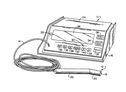
- Referring to Fig. 1, an embodiment of the instrument or
the invention particularly designed for employment in the medical-
surgical field is represented generally at 10. This instrument
- includes a hand-manipular probe represented senerally at 12 which
- is coupled by a triaxial cable 14 to a console 15. The probe 12,
which preferably is reta ned by the surgeon within a disposable
polymerlc sheath or cover is maneuvered about .he region c-
sursical interest t^ loca_e tumerous tissue for resection. ~hen
used in conjunction with colonic surgery, for example, the ~ o~e 12
-- 8 --
1 3374~1
, ~ane1lvered -hr_u~;~ a surg.cal c~eninc in =~.e '~cdy -_v_ty ar.-
essentially br^ugn_ into c_ntac= wi_. or~,a~.s under a~dy ~y _.~
surgecn. When _mplcved in a radiol~LL.uno-guiced mode, 2 l__dspeaker
or annunciator ~ithin the console 16 may be employed .o ~rovide a
"siren" form o^ output which apprises the su-geon tha- the probe 12
is nearing a s-.e o^ cancer. Thus, it is necessary t~at _..e device
12 be of convenient length and comfor~a~le .^ grasp. .h- ~ro~e 12
is seen to include a window 18 located 2t t:-.e tip OL an znsul2rly
criented port_on thereor 20. Por_ion 20 extends fror.i a hand-
lC grippable por. on 22 at an angle of akout 30' to faci''=~te its
manuever~bility about the bac~ or hidcer. side or organs.
Because the assembl2ge 10 is used in a surg ca .hea.er,
the console 15 also is readily cleaned, hzving a smooth, one-piece
toucn sensitive -olymeric surface 24 su~...cunt~ng z relativelY large
LCD readout or displ2y 26, a duai colcrec LED readcu. 28 znd a
seauence of finger-actuated switches hzvins a tac.il- ~edkac';.
These switches ^r k-~yboard as represen_-c sener211y a= 3~ permit
the mlcroprocessor driven console 16 to carr,-cut an ins.-_cti~e or
1 337441
~~ "user friendly" dialogue with the practitioner. For purposes of safety, the
device is po~Jered by a rechargeable battery.
In addition to conventional on and off switches shown, respectively, at
32 and 3~, tlle switches provided on the console 16 include a count mode
5 switch 3~, a sound switch 35, a reset count switch 36, a range function
switch 37, a calibration function switch 38, and up and down incrementing
switches for adjustment within certain of the switch generated modes as
shown, respectively, at 39 and 40.
The probe 12 must be capable of performing essentially at room
10 temperature. Thus, the device employs a cadmium telluride crystal and,
because of the preferred low energy levels of radiation which it may detect,
must be capable of operatively reacting to low energy gamma ray
interactions. The interaction of gamma rays with such crystals is primarily
through three processes, namely the photo-electric effect, Compton
15 scattering, and pair production. In the photo-electric effect, a photon of
energy, hv, interacts with an atom as a whole. Its energy is completely
transferred to an electron, usually in the innermost shell. The electron is
ejected with a kinetic energy: ekin = hv - Eb, where Eb is the binding energy
of the orbital electron, h is Planck's constant, and v is the frequency
20 associated with the wave nature of the gamma radiation. In Compton
scattering, the primary photon may interact with any one of the orbital
electrons. The electrons are considered essentially as free electrons under
the condition that the primary photon energy is large compared with the
electron binding energy. The interaction may be analyzed as the elastic
25 collision between the primary photon and the electron. Energy is shared
between the - recoil electron and the secondary photon. This secondary
photon travels in a direction different from that of the primary photon, and
is referred to as the scattered photon.
Thus, as an incoming gamma ray is absorbed by the crystal, it
30 transfers some or all of its energy to electrons, which as charged particles
pass through the semi-conductor producing electron-hole pairs and,
therefore, the capability of charge-transfer within the crystal medium.
When a charge particle produces electron-hole pairs in the semi-
conductor, the electric field causes these charge carriers to move toward
35 and accumulate at the appropriate electrodes. As these charges are
collected at the electrodes, they induce a charge or electrical pulse signal in
the circuit external to the detector. It is then necessary to pre-amplify
-- 10 --
1 33744 1
these signals and feed them to the electronics of the e^ntrol unit or console
16.
For effective performance, the probe 12 iust be capable of
generating and discerning signals representing gamma .a~ strikes which are
S of extremely low energy. In this regard, a gamma ra~; interaction with the
cadmium telluride crystal may produce two to four thousand electrons. It
being recognized that ~.25 x 1018 electrons per second represent one
ampere of current, the relative sensitivity of the instant device will become
apparent. As a consequence, the mechanical structuring of the mounting
10 arrangement for the crystal within the probe 12 is of critical importance as
is the technique for detecting and treating these significantly small charges
representing gamma ray interactions.
Looking to Fig. 2, a more detailed representation of the probe device
12 is revealed. The angular orientation of the front portion 20 is shown
-- 15 having the noted 30 cant with respect to the central axis of the hand
gripped portion 22. Device 12 is smnll having an overall length of about
19 cm and portion 22 having a length of about 12.7 cm. The overall
diameter of the cylindrical structure 12 is about l.g cm. Front portion 20 is
formed having a groove 42 for retaining a collimator .vhich optionally may
20 be positioned over the portion 20 and window 18 to provide a higher
directional aspect for the device. The hand grip portion 22 carries a
- preamplifier on an elongate circuit board as represented in general at 44.
Depending upon the energies of radiation encountered, the probe 12
structure is formed of an electrically conductive and thus shielding material
25 which further functions to attenuate radiation.
Cable 14 supplies power to the preamplifier of the probe, as well as
bias to the crystal and functions to transmit the preamplifier treated output
signals. Cable 14 includes tin copper cladding components 46 and 48 which
are mutually insulated and spaced by a silicon rubber tube 50 which is
30 somewh~t loose to permit flexure. The innermost leads of the arrangement
at respective lines 52 and 54 carry the output signals from the preamplifier
44 and a bias signal, for example 30 volts, for application to the rear side of
the crystal within the device 12. Clad 46 carries a 12 v power supply for the
preamplifier circuit, while outer clad 48 carries ground for the system. An
35 outer silicon rubber cover then is provided at 56.
Lool~ing to Fig. 3, an exploded detail of the nose or forward portion 20
of probe 12 is provided. This portion 20 retains the cadmium telluride
-- 11 --
1 337441
crystal in a light-tight and mechanically secure orientation while
mQintaining necessary ground and bias conditions upon it. Generally, such
crystals as at 58 will have a rigi~ity or physical consistency somewhat
simliar to cllalk and are formed having very light gold coatings on their
5 surfaces. Device 58 is retained within an outer electrically insulative
coating 60 of U-shaped cross section. The forward or front surface 62 is
grounded and, in effect, represents the most negative electrode in the
system. Its rearward face 64, Oll tlle other hand, has a bias, for example
30 v, applied to it, an available bias range of lOv to lOOv generally being
10 desired. Thus, these electrical parameters are required with respect to the
crystal 58 while it is maintained in a carefully electrically shielded,
acoustically dead and light-tight environment. The outer surface of front
portion 20 is an electrically conductive tube or collar 66 formed, for
e~ample, of copper so as to provide an electrical shield as well as an
15 attenuator for radiation of the energy range contemplated. The forward
edge of tube 6B is closed by tlle window 18 whicll is formed of a silicon-
aluminum alloy about 0.015 in. thick soldered thereto.
Crystal 58 and various components associated with its mounting are
assembled within the cup-shaped structure including window 18 and shell 66
20 in a sequence represented in Fig. 3 which includes a foamaceous,
electrically conductive insert G8 llaYing a diametric e.Ytent such that it is incontact with ground, here the internal electrically conductive surface of
shell 66. Generally, the insert 68 may be provided as a carbon impregnated
foam wllic}l functions to assist in the compression of the components under
25 final assembly. Insert 68 is shown in Fig. 3 exhibiting its expanded, pre-
assembly cross-sectional configuration.
Next in the assembly sequence is a disk-shaped insert 70 formed of
carbon filled silicon rubber having a thickness, for example, of 0.020 in. The
diametric extent of the insert 70 is such that it is in contact with electrical
30 ground about the internal periphery of the tube portion 66. Marketed, for
example, by Tecknit Company of Cranford, New Jersey, insert 70 is both
pliant and e~chibits an adhesive-like surface which, in final assembly, tends
to adhere to the forward surface 62 of the crystal 58. It has been found that
the use of this disk, substantially improves the noise immunity of the device.
3~ Thin aluminum foil has been employed in place of the carbon illed rubber
for insert 70, however, any slight rubbing of the foil insert against the face
62 will create a static electricity build-up and, thus, noise. While
1 337441
~_ considerable improvement was fourld in emplo~ing tlle aluminum disl~, it also
was îound that the probe functioned only wherl held motionless during a
count, the mere sliding of a fingertip across the surface of the probe causing
unacceptable noise levels with the latter arrangement. A similar disk of the
5 conductive silicon rubber materiai but o~ lesser diametric extent is
positioned for engagement with the rearward surface 64 of the crystal 58 as
represented at 72. The noted crystal bias voltage is asserted through this
adllesive surrace insert 72 from a disk-shaped copper electrode 74. Provided
llaving a thickness, ~or e~ample, of about 0.050 in., the electrode 74 may be
10 gold-plated at least on its contact surface to improve conduction and avoid
corrosive effects. The rearward side of the insert 74 carries a bead of
solder ~G to effect a union with a short length of insulated wire 7~. The
assemblage of crystal 58, insert 72, and electrode 74 is configured to nest
within an insulative cup 80 formed, for e~cample, of Teflon or the like. Cup
15 80 is configured having a hole 82 at the center point thereof for the purposeof receiving wire 78 and accommodating solder bead 76. To assure removal
of all ionic contaminants, cup 80, shell 66 and window 68 are boiled
repeatedly in distilled water prior to assembly.
Cup 80 and its internested components are slideably retained within a
20 cylindrical cavity 84 bored within a slug or blocking component 86. Formed
having a principal diameter which is slideable within the tube 66, the slug ~6
is fashioned of copper or tungsten or the lil~e and functions both to provide a
secure support for the crystal mounting components and to assure radiation
blockage with respect to any radiation impinging from the rearward portion
of the probe 12. Component 86 is counterbored at 88 to accommodate for
the solder bead 76 upon assembly. Communicating from counterbore 88 is a
bore 90 of small diameter selected to receive the small wire 78 which
extends to an electrical connector 92. Connector 92 is covered with an
electrically insulated material and is slideably inserted into bore 9Q, the
outer head portion thereof at 94 residing within a counterbore 96 within
component 86. Blocking or bacl~ing component 86 additionally is configured
having a coupling portion of lesser outer diameter 98 which is configured to
be slideably received witllin the internal diameter of a supporting tubular
portion 100. The forwardly disposed tubular region of portion 100 at 102 is
configured having a diameter to, in turn, coincide with that of the main
diametric component of slug 86 so as to slideably receive tubular portion 66
upon assembly. Upon such assembly, as shown in Fig. 2, an additional
-- 13 --
1 337441
~, retainer groove us at 1(1~ is developed. ~or assembly, additionally, a
connector wire us at 106 pro~ddes elcctrical connection between connector
92 nnd the preamplirier 44 (Fig. 2).
The sub-assemblQge of electr~de 74, cup 80 and slug componcnt 86
5 along with connector 92 is provided prior to a final combination of the
forward probe part. In this regard, it is desired that the wire 78 be
maintained in tension to assure no mechanical movement in the sub-
assembly. To provide this, tlle wire is coupled to the connector 92 and
supported so as to extend througll bore 80 and into contact with the solder
bcad 76 within the cup 80. Cup 80 will have been positioned along with the
electrode 74 within cavity 84. The disk electrode 74 then is heated such
that a sweat soldering of the wire tal~es place and connection is made with
the components in a heated state. Upon cooling, the resultant assemblage
provides for the wire remaiIling in tension to secure against component
15 molion. l~n avoidance of any relative motion of the components is
important because of the cnpacitive effect developed with any relative
- motion between the components of the assemblage. The noted sub-assemblage along with the remaining components described in connection
witIl Fig. 3 then are "slid" together under a dry nitrogen atmosphere.
20 - Lool<ing to Fig. 4, the components shown in expanded form in Fig. 3
are represented in their post-assernbly orientations. Note that the
foamaceous insert G8 has been compressed to aid in securing the remaining
cofnponents from any motion. The foam material is compliant in this regard
to assure a uniform compression of all components into the crystal 58.
25 Similarly, the slightly adllesive and compliant silicon rubber inserts 70 and72 aid in this securement. Components 100 and 6G may be retained
togetller, for example, USillg an epoxy adllesive. ~s noted earlier, the
mildest of vibrational movement may create a capacitive alteration on the
order of a gamma strike for the very delicate instrument. Thus, the
30 arrangement shown serves to provide mechanical securement. There also is
a potential for vibration and tlle noise dif ficulties that ensue due to the
microphonic effects occasioned by the occurrence of noise or the mildest of
disturbance at tlle window 18. I;oamaceous material 68, as well as the
inserts as at 70 provide a protection for such effect due to the change of
35 acoustic impedance. For example, any microphonic effects at the window
surface 18 will be damped by the change of acoustic impedance at the
junction between window 18 and foamaceous material 68. A similar
1 33744 1
~_ alteration occurs between the insert (;8 and the ne~t subsequent silicon
rubber insert 70. This alteration Or acoustic impedance is analogous to the
difficulties in vocally communicating from the atmosphere to a listening
position benenth the surface of water. Generally, the principal source of
5 microphonics e~fects is occasioned with rubbing at the surface of window
18, a condition to be encountered in normal operations. Of course the
maintaining of tubular portion 66 and the entire housing of the probe
including components 100 and handle 22 at ground reference functions to
provide an electrical shielding. It has been found helpful to dampen acoustic
10 vibration of window 18 by applying a polymeric coating to its outside or
inside surface, i.e. Teflon or the like.
~ Referring to Fig. 4A, an alternate and effective arrangement of the
forward portion 20 of the instrument 12 is portrayed in silTiilar fashion as
Fig. 4. In the figure, a disl~ of the earlier-described electrically conductive
15 silicon rubber 71 is positioned against the inner surface of window 18. The
opposite face of tllis insert 71 then confronts a dead air space 73 which, in
turn, extends to an assemblage comprising the earlier-described electrically
conductive foamaceous material 68, rubber insert 70 and crystal 58. These
components are retained compressively together by a band 75 which is
2~ structured of a material permitting the transmission of gamma radiation
therethrough but which, preferably, additionally is electrically conductive.
~luminum, for e~cnmple, may be used for the band 75. The remainder of the
- structure is identical with the structure of Fig. 4 as labelled with the same
numeration. Providing a uniform resistance from the forward surface of
25 crystal 58 to ground is an important aspect of each of the embodiments
shown in Figs. 4 and 4A.
Referring to Fig. 25, a preferred structur;ng for the forward portion
20 of the instrument 12 is portrayed in similar fashion as Fig. 3. The
embodiment shown has been found to be more readily fabricable, while
30 maintaining requisite performance characteristics. Fig. 25 shows the hand-
graspable portion as at 22 extending to earlier-described supporting tubular
portion 100. The forwardly disposed tubular region of portion 100 including
surface 102 are configured llaving an internal diameter defining a cavity
1232 for receiving a generally cylindrically shaped slug or blocking
35 arrangement 1230 along with an elastomeric retainer layer which retains the
slug 1230 within the cavity 1232 while spacing its outer cylindrical surface
from the interior wall of portion 100 an amount sufficient to provide a shock
1 33744 1
'_ mounting nrrungement. Tl~is elastorner may be provided, ~or e~cample, as a
rul~ber epoxy rnnteri~l. To ac!lieve spacing ~rom thc noted interior wall n -d
facilitnte mounting, ~n elastomeric ring such as an O-ring is provided as at
123~ which serves to hold the slug 1230 in an appropriate position while the
5 elastomeric rubber epoxy sets. The O-ring 1234 is slid over the copper outer
cylindrical surface Or slug 1230 so ns to nest in a rectangular groove 1236
formed therein. Lool;hlg additionnlly to Fig. 2B, the O-ring 1234 is seen in
assemble(l position and the elastomeric retaining layer is shown at 1238. As
be~ore, slug 1230 is formed of copper or tungsten to attenuate radiation
10 impinging from a rearward direction and further includes a V-shaped groove
- 1240 extending thercabout. /~ central bore 1244 ectends tllrough the slug
1230 to carry insulative lead 106. The forwardmost face of slug 1230
provides a base support sur~ace as ut 12~6 which is coun~erl)ored at 12~8 so
as to provide an improved connection with a plastic electrically insulative
cup or support 1250 havi;lg a rearwardly disposed cylindrical portion 1252
which is nestable within the bore 1248. Cup 1250 may, for example, be
forrned Lexan or the like flnd, preferably, are adhesively attached to the
base support surface 1246 and counterbore 1248 by a compatible adhesive.
Cup 1250, as before, includes a central cylindrical cavity 1254 which
20 receives and supports an assemblage including a resiliently compressible
shock cushion layer 1256 as an initial component. Layer 1256 may, for
example, be formed a non-woven Teflsn clotll marketed under the trade
designation "Gortex" having a thickness, for example, o~ about 0.020 in. The
layer 1256 is provided having an opening in the middle thereof for receiving
the lead 106. In general. this lead 106 is formed of a multi-strand type lead
and the strands thereof are attached to a small disc 1258 of adhesive copper
tape. This disl~ 1258 serves to electrically couple lead 106 to and apply a
biasing vollage to the rearwardly disposed face 1260 of a gamma radiation
responsive crystal 1262 formed, as described above, oî cadmium telluride or
the equivalent. The forward race of crystal 1262 as at 1264 is electrically
grounded by a copper ground strap 126G which extends rearwardly to provide
electrical grounding communication with the exterior of copper slug 1230.
The assemblage o~ crystai 1262, copper adllesive tape or disk 1258, shock
cushion layer 125B, and cup 1250 are compressively retained togetller by an
elastomeric retainer 1268 which may be provided, for example, as a common
finger cot. This sheath o~ electrically insulative elastomeric material is
rolled over the assemblage and retained in position by a resilient band such
-- 16 --
1 337441
as a resilient O-rh~g 1270. This O-ring nests in the earlier-described V-
shaped circumferential groove 1240 to retain the sheath 1268 in position.
The entire assernblnge of slug 1230 and those parts compressively retained
in position by the slleath 1268 and O-ring 1270 may be maneuvered during
5 the assemblage employing rubber epoxy layer 1238 to provide appropriate
spacing accom modating for variations in component thicknesses, for
e~ample the thickness variations which may be encountered with crystal
1262. The forward assemblage inclwding tube 66 and window 18 then is
positioned over surface 102 and cemented in place, ~or example, with a
10 conductive silver epoxy cement. Note in Fig. 26 that the assemblage is so
oriented that a dead space 1272 is created between the forwardly disposed
surface 1264 of crystal 1262, as associated with retainer sheath 1268, and
window 18. This de~d air space provides an enhancement of acoustic
isolation of the crystal 1262.
As represented at circuit board 44 in Fig. 2, in order to carry out the
treatment of the very faint charges which are evolved due to gamma
interaction with crystal 58, it is important that the preamplification
function talce place as close as possible to the situs of the interaction.
Because of the operational need in surgery for the 30 cant of the central
20 axis of the forward portion 20 witll respect to the corresponding axis of the rearward support portion 22 of the probe 12, some small length of
transmission wire as at 106 is required. Because extremely small charges of
current are involved in the range of 300-600 atto coulombs, a
- preampliication stage which performs to achieve a very high gain is called
25 upon but one which performs with low noise generation. In effect, the
preamplification stage of the instant apparatus is one achieving a voltage
amplification, for example on the order of about 25,000. Correspondingly, if
one considers the current amplification function numbers of electrons
constituting very faint charges are converted to about a milliampere at the
30 output of the preampli~ication stage, an enormous gain condition (about
three trillion). The resultant power gain is about 8 x 10¹⁶.
Loolcing to ~ig. 5, a preamplifier circuit represented generally at 110
employed with the instrument 12 is revealed. In the figure, earlier
described input line 54, carrying the bias for assertion at the rearward face
35 of crystal 58 again is reproduced as extending to one side of crystal 58
through resistors Rl and R2. Resistor Rl in combination with a capacitor
Cl provides a local filter to remove any spurious noise which may be
1 337441
~" engendered in tlle line transmitting tlle noted bias signal. The opposite face
of crsytnl 58 is coupled to ground as represented at lines 112 and 114. In
gcneral, the preamplifier circuit 110 includes an integrator stage
represented generally at 116 wllich is followed by a voltage am?lification
and line driver stage represented generally at 118. Integration stage 116 is
formed of three transistors identified at Ql-Q3 performing in conjunction
with a capacitor C3.
The input to stage 116 from crystal 58 includes a crystal bias resistor
R2 of very large resistance value, for example about 50 megohms, a level
selected to avoid absorbing current disturbances from crystal 58. Generally,
the resistance for this component will be selected between about 10 to 200
megohms. The input signal to the integration stage 116 at line 120,
typically about 300-600 atto coulombs, is asserted through coupling
capacitor C2 to the gate input terminal of an N-channel junction field
effect transistor (JFET) transistor Ql. Line 120 also is coupled via line 122
and bias resistor R3 to ground at line 112. The resistance value at resistor
R3 is selected commensurately witl1 the selection of resistance for resistor
R2, preferably at about 200 megohms to avoid signal absorption. Generally,
the resistance for this component will be selected between about 10 to
10,000 megohms, the component supplying bias for transistor Ql. Also
extending from line 120 at the input to the integrator stage is line 124
leading to a coaxial capacitor C3, the opposite side of which is coupled to
integrator stage feedback line 126. Capacitor C3 is very small, typically
having a capacitance of 0.25 picofarads and, in general, having a
capacitance less than one picofarad. To create this capacitor C3, copper
tubing having a 0.050 in. outside diameter is employed in conjunction with
an insulated wire inserted in its center. Wire 126 is soldered to close the
opposite side of the tube. Thus, by moving wire 124 inwardly and outwardly
of the surrounding tube coupled to wire 126, the capacitive value at
capacitor C3 may be altered. Capacitor C3 may be tuned in the above
manner to adjust the preamplification stage 110 for gain. Such construction
of capacitor C3 may be referred to as "coaxial".
JFET transistor Ql functions, in effect, as a "source follower~' charge
amplifier, its purpose being to achieve an impedance transformation from a
very high impedance gate suited to low current and low noise. In general,
the JFET structure exhibits lowest current noise at the room temperature
operating conditions contemplated for the instant instrument. Further,
1 33744 1
these devices e~!libit high fre~uency response (wide bandwidth) as well as a
high amp1i~ication ~actor or high transconductance. In view of the latter
aspect, the device tends to create a large current disturbance at its source
terminal at line 128. Line 128 extends through a source load resistor R4 to
5 ground line 112. Tlle resistor R4 functions as a d.c. current return device.
The drain terminal of transistor Ql is coupled to +12v supply via lil~e 130,
while the same terminal is decoupled or isolated by a filter comprised of
capacitor C4 and resistor R5 connected with line 130.
The signal related voltage at line 128 is coupled via line 132 to the
10 base of NPN, bi-polar transistor Q2. Transistor Q2 performs a voltage
amplificntion and a singular bi-polaF component is elected for this function
inasmuch as such devices e:~hibit low voltage noise characteristics at room
temperatures. Additionally, the devices have a higher amplification factor
availability than corresponding field effect transistors. The use of such a
15 bi-polar device in conjunction Wit}l the input field JFET device was evolved
following significant experimentation and represents a lowest noise
combination which was achieved in conjunction with room temperature
operation.
The degree of amplification achievsble with the stage Q2 is related to
20 the impedance exhibited with respect to its emitter and collector, i.e. the
value of the collector load impedance divided by the emitter impedance. In
the arrangement shown, the emitter of transistor Q2 is coupled via line 134
to ground through resistor R6 and, importantly, the emitter is by-passed to
ground via lines 134 and 136 through capacitor CS. The latter component
25 exhibits relatively low impedance on the order of 25 ohms at the frequencies
of interest. Looking to the collector to supply arrangement at line 138,
there is a relatively high resistance value resistor R7, for example of
3 ~ohms and, in series, a resistor R8 having a 1.5 I~ohms resistance to
provide a total resistance of 4.5 Kohms. To achieve the most effectiYc
30 amplification or highest gain, NPN transistor Q3 is so coupled within the
integrator stage 116 as to provide a "boot strap" circuit to raise the
ef~ective collector impedance to transistor Q2. In this regard, the base of
transistor Q3 is coupled via line 140 to line 138, while the collector thereof
at line 142 is coupled to supply line 130 in conjunction with a decoupling
35 filter comprised of resistor R9 and capacitor C7. The emitter of transistor
Q3 is coupled to line 126 as well as to line 144 to ground through re~istor
R10. Line 126 is seen to e~ctend to line 146 incorporating capacitor C6 and
-- 19 --
1 33744 1
l,~ coupled intermediate resistors R~ and R8. Transistor stage Q3 functions as
- an emitter fo11Ower, feeding tlle noted junction between resistors R~ and R8
through capacitor C6 in boot-strapping fashion. The result is to raise the
effective impedance at the collector of transistor Q2 due to the alteration
of net current flow througll resistor R7. This provides a much higher
voltage gain achieved at the integrator stage 116. Note that a portion of
the signal from the emitter of transistor Q3 returns to the coa~ial capacitor
C3 of the integrator stage.
Voltage amplifier and line driver stage 118 is seen to be comprised of
an a.c. voltage ampliEier configured as the combination of NPN transistor
Q4 and PNP transistor Q5. Such an arrangement comprises desirably few
components and exhibits high gain and very broad bandwidth. Because the
gamn~a ray interaction of crystal 58 will e2chibit a frequency disturbance
spectrum ranging from about 50 KlIz to 200 KHz the frequency response of
the stage 118 is tailored accordingly. ~or example, the high end roll off of
this response is established by resistor R10 within line 144 and capacitor C8
within line 148. The output of the integrator stage is asserted through
resistor Rll and capacitor C~ to the base of transistor Q4. A voltage bias
to the base of transistor Q4 is provided via line 148 from supply following its
division by divider resistors R12 and R13. This bias input, amounting to
about one-fourth of the supply voltage also is treated by the filter
combination of resistor R9 and capacitor C7.
The 12 v power supply additionally is filtered by a pi filter comprised
of capacitors C10 and C12 along with resistor R14 connected within line
150. Line 150, in turn, is seen to e~tend via line 152 to the emitter of
transistor Q5 and through resistor R15 to the base thereof as ~ell as to the
collector of transistor Q4. Correspondingly, the emitter of transistor Q4
extends via lines 154, 156 and 158 to resistor R16 and the collector of
transistor QS as well as to resistor R29. The output of stage 118 is provided
at line 168 incorporating resistor R17. The gain of this output stage is set
by resistor R18 within line 154 in conjunction with resistor R16, while
capacitor Cll in that line aids in the setting of low frequency roll-off of the
stage. The high frequency roll-off characteristic is further aided by the
combination of resistor Rll and capacitor C13, the latter component being
coupled between line 145 and ground via line lG2. Low end roll-off
characteristics for the stage further are aided by the combination of
capacitor C5 and resistor R6.
-- 20 --
~ 337441
~, In view of the extreme sensitivity of the type of prearnpli~ier at hand
nnd the tcndency of such circuitry to oscillate, the layout o~ the circuit
within housing portion 22, for example on a circuit board as at 44, also
becomes an important nspect in the design of the instrument. Thus, looking
5 to Fig. 6, a layoul for the preamplifier circuit showing component
orientations and relative positioning is revealed. In general, the most
sensitive components are grouped to the left in tlle figure, a position
corresponding with a left orientation in conjunction with Fig. 2. As a
consequence, tllese components are closest to the crystal in the system.
10 Because of the very large resistance values ~or resistors R2 and R3, these
resistors are to the left in the circuit orientation and are mounted vertically
upwardly from tlle board or base, one side of them being attached at such
base. Tlle opposite sides of these resistors extend in space to couple to
cnpacitor C2. Thus, capacitor C2 is off the surface of the printed circuit
15 board to avoid leakage conditions. The most sensitive transistor in the
system is JFET transistor Ql whose source and drain terminals are coupled
to the printed circuit board, while its gate electrode extends to the common
junction in space of capacitor C2 and resistor ~ 3. Thus, this sensitive
terminal also resides in space in close proximity to the crystal itself.
20 Coa:cial capacitor C3 is mounted upon the board in a vertical orientation
sucl- that it~s tuning wire line 124 is coupled from its coaxial location withinthe component to the common juncture of the gate of transistor Ql and tlle
upstanding common junction of resistor R3. The above-described are the
most sensitive of the components and their mounting in the manner shown
25 has been found to be important to successful operation of the device.
Capacitor C18 is a radial-lead device and is seen coupled to the left side of
the circuit board for convenience as may be observed by looking to its
corresponding position in Fig. 5. Note that the component developing the
highest amplification effect, transistor Q5, is furthest to the right on the
30 circuit board away from the sensitive gate at transistor Ql. The remaining
components are shown in their orientations on the circuit board 44 along
with small lines representing the "hair pin" type mounting orientations.
Referring to Figs. 7A and 7B, a block diagrammatic representation of
the instrumentation circuitry is revealed. In Fig. 7A, the cadmium telluride
35 crystal 58 again is shown having one ace coupled to ground through line
170, while the opposite, biased face thereof is coupled via lines 172 and 174
to a bias filter represented at block 176. As noted above, this filter, for
-- 21 --
1 337441
~_ example, includes resistor R2 as well as capacitor Cl and resistor Rl. The
input to the ~ilter components 17G is represented at line 1, 3 as being applied
through the triaxial cable as described earlier at 1~ and re?resented by that
numeral herein. Line 178 corresponds with the earlier-described line 52 in
5 I;ig. 2. This bias emanates from a power supply shown at block 180 in Fig.
7B and represented at line 182.
Line 172 from the crystal 58 is shown extending to the earlier-
described integrator stage of tlle prcampliEier 110. The integrated valuation
of detected radiation disturbance then is shown directed, as re?resented by
line 184, to the driver-amplification network described generally at 118 in
Fig. 5 and identified by that numeration in block form in Fig. 7A. A 12 v
power supply is provided from the power supply 180 (Fig. 7B) as represented
at line 186 which, as shown in Fig. 7~, is directed to a probe current
network represented by block 188. Under microcomputer control as
represented by line 190, the network }88 develops signals, for e:~ample,
determining whether the probe instrument 12 has been properly connected
to the console 16. Delivery of the 12 v power supply for the preamplifier
stage 110 is represented at line 192 as extending to the driver amplifier
-from cable i4 via line 194. Line 194 corresponds with the clad 46 described
20 in conjunction with cable 14 in Fig. 2.
Ground to the instrument 12 also is developéd from the power supply
block 180 as represented at line 196 shown in Fig. 71~ as extending to cable
14 and via line 198 to the instrument and preamplification components 110.
Line 198 corresponds with the earlier-described clad at 48 in Fig. 2.
The output of the preamplification circiut 110 is represented at line
200 extending through the cable representation 14 corresponding with the
earlier-described line 54 in Fig. 2. Line 200 extends from the cable 14 as
line 202 to the input of a normalizing amplifier represented at block 204.
The network represented by block 204 functions to amplify or attenuate, i.e.
scale the noise characteristic of any given instrument 12 and normali2e the
value thereof or render it consistent for later comparison stages. Generally,
for example, the 27 kev energy level gamma ray generated pulses in the
system will be about five times higher than noise levels. Normalizing
amplifier network 204 will establish those noise levels at some
predetermined level, for example, 200 millivolts and the resultant
proportional valid gamma related pulses will become about one volt high for
purposes of ensuing comparison functions. It may be observed that the
-- 22 --
1 337441
~, amplifier networl~ at block 204 is shown controlled from a digit~l-to-an~log
converter network re?resented at block 206 via line 208. Network 206, in
turn, is controlled from line 210 e:Ytending, as shown in Fig. 7B to block 212
representing a microcomputer network. The normalized output developed
from network 204 is presented along lines 214 and 216 to a noise averager
circuit as represented at block 218. This network, represented at block 218
determines an average amplitude value for the noise of a given system with
a given instrument 12 and provides a corresponding signal as represented at
line 220 (noise amp) which is empl~yed as above-described as information
used by the microcomputer 212. This information in addition to being
employed with the normalizing amplifier network represented at block 204,
may be employed to develop a low window valuation for the comparison
func tion.
Line 216 also extends via line 222 to a pulse acquire network
represented at block 224. This network functions, when activated by the
microcomputer represented at block 212, to acquire the value of the highest
pulse amplitude witnessed at line 222. Periodically, this information then is
transmitted to the microcomputer at block 212 as represented by line 226.
Representing a rorm of peak detector, the network is sometimes referred to
as a "snapsllot circuit". Also produced from line 216, as at line 228 and
block 230 is a buffer amplifier which will provide at line 232 an output
representing received pulses which may be made available at the rearward
portion of console 16 for conventional radiation evaluation purposes.
Line 214 extends, as shown in Fig. 7B at line 234, to one input of an
upper window comparator represented at block 236 and a lower window
comparator illustrated at block 238. The threshold levels for comparative
purposes employed by the network at block 238 is shown asserted from line
240 and, preferably, is developed by the logic of microcomputer network 212
at a level just above the noise amplitude signals generated from line 220.
Of course, manual setting of such windows can be carried out. In similar
fashion, the upper window of acceptance for valid gamma ray interaction is
established from a corresponding line 242. This threshold setting may be
made from the information taken from pulse acquire network 224.
Returning to Fig. 7A, the threshold upper window and lower window
threshold selections are made under the control of the microcomputer
network at block 212 as controlled from the digital-to-analog network shown
at block 206. It is the characteristic of such networks as at block 206 to
-- 23 --
1 337441
provide an output which is comprised, for e~ample, o~ 256 ,teps o~ varying
arTpIitude. The percentage of incrementation from step-to-step will vary
somewhat over the range of voltage values provided. ~ccordingly, the
outputs rrom this conversion network at block 206, as at lines 244 and 246
are directed to squarer networks shown, respectively, at blocks 248 and 250.
These networks function to square the current outputs at lines 244 and 246
and thus acllieve a uniform percentage incrementation of the threshold
defining outputs at lines 240 and 242.
Returning to Fig. 7B, tlle outputs of the comparator networks sllown at
blocks 236 and 238 represent candidate pulses which may be above or below
the given thresholds and are identified as being presented as a "UW pulse"
and an "LW pulse" along respective lines 256 and 258. These lines are shown
directed to a real time pulse discriminator network represented at block 2G0
which carries out Boolean logic to determine the presence or absence of
15 - valid pulses. Valid pulses are introduced to the microcomputer network 212
as represented by line 262.
The microcomputer represented at block 212 performs under a number
of operational modes to provide both audio and visual outputs to aid the
surgeon in locating and differentiating tumorous tissue. In tlle former
regard, as represented at line 264 and block 266, a volume control function
may be asserted Witll amplitude variations controlled from a solid-state
form of potentiometer as represented at line 268 and block 270. Further, a
"siren" type of frequency variation may be asserted as represented at line
272 to an audio amplification eircuit represented at block 27~ for driving a
speaker as represented at 276 and line 278. With the noted siren
arrangement, the frequency output from speaker 276 increases as the
instrument 12 is moved closer to the situs of concentrated radiation. Of
course, conventional clicks and beeps can be provided at the option of the
operator.
The microcomputer network 212, as represented by arrow 274 and
block 276 also addresses an input-output network wllich, as represented at
arrow 278, functions to provide a pulse count output of varying types as well
as outputs representing volume levels, pulse height, noise levels and battery
status. Visual readout is represented in Fig. 7B as a block with the same
display 26 numeration as described in conjunction with Fig. 1. Similarly, the
input-output function represented at block 276 provides appropriate
scanning of the keyboard or switches described in conjunction with Fig. 1 at
-- 24 --
1 337441
~_ 30 and represented by the same numeration in Fig. 7B. During a countingoperation, the microcornp~lter network 2 L2 functions to control a light
emitting diode drive network represented by block 282 from line 284. The
drive network reprcsented at block 282 is s~lown providing an input, as
5 represented by line 28G to the dual LED display as described at 28 in Fig. 1
and represented in block form with the same numeration. This readout
provides a red light when a gamma ray is detected and a green light during
the counting procedure in general. A serial output port of conventioanl
variety also is provided on the console 16, such ports being represented at
block 288 being addressed frorn the microcomputer at block 212 from line
290 and having output and input components represented by arrow 292. A
real time clock-calendar having a non-volatile memory also may be provided
in conjunction with the functions of the microcomputer network 212 as
represented by block 294 and arrow 296. Further, the microcomputer may
15 be employed to monitor the performance of the power supply represented at
block 180. This is shown being carried out by the interaction of the
microcomputer network with a multiple.Yer represented at block 298 and
having an association represented by arrows 300 and 302. It may be
observed that the power supply also provides +5 sources for the logic level
20 components of the circuit as represented by line 304; a -5v source at line
306, as well as a -9v reference at line 308 for display 26 drive and, finally, a- 2.5 v reference as represented at line 310 to provide reference input to the
analog circuitry described later herein.
Returning to Fig. 7A, the microcomputer network as represented at
25 block 212 also prov~des an input to the digital-to-analog conversion network
represented at block 206 which corresponds with the instantaneous pulse
rate and this information is conveyed to a pulse rate amplifier network
represented at block 312 via line 314. The resultant output as represented
nt line 316 may be provided, for~e:~ample, at the rear of the console 16.
3~ This circuit represented at block 312 also may be employed to generate a
calibrating pulse for testing the downstream components of the system.
Thus, the microcomputer applies a predetermined pulse level through the
digital-to-analog conversion network at block 206 for presentation to the
amplifier network represented at block 312. The resultant output at line
318 is selectively switched as represented by block 32û to define pulse width
from the microcomputer input at line 322 to generate the calibrating pulse
at line 324.
-- 25 --
1 33744 1
Referring to l; igs. 8/~-8C, pulse treqt,ng analog circuits as are
maintained in console IG are revealed. In Fig 8A, the output of a 10 pin
ribbon cable which, in turn, is coupled to trinxial cable 14 is revealed
generally at 330. Of the ten connecting pins and lines of this ribbon cable,
5 five are at ground for shielding purposes as re?resented by ground line 332.
The bias supply is provided ~rom the earlier-described power supply as at
blocl~ 180 and shown again at line 182 extending through resistor R20.
Corrcspondingly, the +12v power supply earlier described at line 186 again is
reproduced as extending to the terminal 330 through resistor R21. Lines 182
and 186 are seen coupled to respective filtering capacitors C16 and C17.
FiIlally, the preamplified detector pulse output is received from the
connector 330 from along line 332 and is applied to the analog downstream
circuitry through bloclcing capacitor C18.
The probe current detector described earlier in conjunction with block
188 in Fig. 7A again is represented in general by that numeral in Fig. 8A.
This detector employs resistor R21 within -12v supply line 186. The
opposite sides of resistor R4 are tapped at lines 334 and 336 which, in turn,
are directed to a resistor network comprised of resistors R22-R25 and
tllence are directed to the inputs of an operational amplifier 338. A
filtering capacitor Cl9 additionally is coupled to one side of resistor R21.
The resistor network R22-R25 and amplifier 338 form an instrumentation
amplifier which measures the voltage difference across resistor R21 and
further functions to perform a level shift of 12v to ground. Following such
level shifting, the resulting probe current resDonsive signal at line 340 is
directed to the non-inverting input of a second amplification stage 342.
Stages 338 and 342 are shown coupled to +12v as filtered by capacitor C20
via line 344 and to -12v supply as filtered by capacitor C21 via line 346.
The inverting input to amplifier 342 at line 3~8 incorporates resistor R26
and, additionally is coupled to the output of stage 3~2 at line 350 via
resistor R27. Amplification stage 342 functions to amplify the signal from
stage 338 by a factor, for example, of 10 to provide an analog signal
representative of probe current (PROBE I) at line 352. This analog signal is
directed to the microcomputer function earlier described at block 212 in
Fig. 7B.
Line 202, carrying the preamplified gamma reaction pulses is directed,
as shown in Fig. 8B, to the input of the normalizing ampli Eier network
represented in Fig. 7A at block 204 and shown in general by that
-- 26 --
1 33744~
numeration. The signal at line 202 is filtered by a capacitor C22 while a
resistor R27 supplies bias to P~P transistor Q~. These filter components
provide a high fre(luency roll-off avoiding R~ interference which may be
encountered. The collector of transistor QG is coupled via line 352 and
5 resistor R28 to -5v supply, while the emitter thereo~ at line 35~ is coupled
through resistors R29 and R30 to +Sv supply. Resistor R30 provides a supply
- bypass filter function in conjunction with a capacitor C23 coupled with line
354 via line 356, while resistor R29 provides emitter bias for transistor QG.
~urther filtering for line 35G is provided by capacitor C23. This relatively
stable supply at line 356 is directed via line 358 to line 360 e~ctending in onedirection to the collector of NPN transistor Q7 and in the opposite direction
througll collector load resistor R31 to the collector of NPN transistor Q8.
Transistors Q7 and Q8 are coupled as a differéntial pair"laving a common
emitter connection at line 362 which e.Ytends via line 364 to the collector of
NPN transistor Q9. The base of transistor Q9 is coupled by line 364 to line
352, while the emitter thereo~ is coupled via resistor R32 to -Sv. The high
pass filter comprised of capacitor C24 and resistor R33 additionally is
coupled from the emitter of transistor Qg to -Sv.
The base of transistor Q7 is coupled to ground via line 366, while the
corresponding base of opposite transistor Q8 is coupled via line 368 to the
digital-to-analog control described in connection with block 206 in Fig. 7A.
r,ine 368 will receive a controlling current as directed by the microcomputer
network 212 to carry out a normalization process. Line 368 additionally is
coupled with a voltage dividing network comprised of resistors R34 and R35,
the former resistor being positioned within line 370 and the latter within
line 372. Note that line 370 is directed to ground. As a consequence a
slight bias voltage is applied to the base of transistor Q8 as is further
filtered by capacitor C25. Capacitor C26 within line 374 functions to filter
ground line 370 from -5v supply.
The collector of transistor Q8 is coupled via line 376 and coupling
capacitor C27 to the inverting input of an operational amplifier 378. The
non-inverting terminal of the amplifier is coupled to ground, while power
input to the device 378 is developed from +5v supply via line 380 and from
-5v supply via line 382. A capacitor C28 filters the latter line. The gain set
and high frequency roll-off characteristic of amplification stage 378 are
derived by the feedback path sllown at line 384 incorporating resistor R40
and capacitor C31 to provide an output at line 386. With the arrangement
-- 27 -- -
1 337441
shown, the a.c. signal applied to the base of transistor Q5 becomes a
fluctuating current at its collector which is referenced against -5v supply.
- There develops in conse~uence an a.c. signal across transistor Q9 which
creates a.c. current in its collector. That ~.c. current is split along two
5 paths associated with diE~erential transistors Q7 and Q8. ~3y controlling the
current input from the digital-to-analog converter at line 368, the d.c.
voltage at the base of transistor Q8 may vary above or below ground. ~here
it varies below ground, the a.c. signal into the collector of transistor Q8 is
- diminished and, conversely, if that value is above ground the current is
lû starved îrom the collector of transistor Q7 and accentuated at transistor
Q8. Operational amplifier 378 buffers the resultant signal conditioning and
applies it as raw pulse data to line 38~. In operation, the microcomputer
function described in conjunction with block 212, evaluates tlle noise
amplitude at line 220 (Fig. 7B) and adjusts the signal at line 368 such that
the noise condition achieves a nominal consistent value, notwithstanding
that different probe instruments as at 12 may be employed. This assures
performance at the upper and lower window comparator functions described
in conjunction with blocks 236 and 238 in Fig. 7B whiell is consistent and
proper from probe-to-probe.
The raw pulses at line 38G are directed, inter alia, through frequencg
shaping elements including resistor R41 and capacitor C33 in line 388 to a
buffer stage described in conjunction with blocl~ 230 in Fig. 7A which is
formed of an operational amplifier 390. The non-inverting input of the
- amplifier is coupled to ground while additional frequency shaping in gain
elements thereof are provided in feedback fashion from the output line 392
of the amplifier via line 394 to line 388. This feedback path incorporates
resistor R42 and capacitor C34. The amplifier stage 390 is powered from
+5v via line 396 coupled to +Sv which is filtered by capacitor C35 and is
coupled to -5v supply from line 398 which is filtered by capacitor C36. The
3~ resultant output, as presented through resistor R43, may be employed for
peripheral devices such as oscilloscopes and the like wherein the buffered
raw pulse data may be analyzed.
Line 386 extends additionally via line 400 to the input of comparator
stages described in conjunction with blocks 236 and 238 in Fig. 7B and
identified in general by the same numeration in Fig. 8B. These stages are
essentially identically structured and thus, identical numeration is employed
-- 28 --
1 ~37~
in their description but with primed notation in conjunction with the circuit
at ~38.
The compnrator stage 236 is formed of a type LTlOllCN8 comparator
- as at 404 into which the negative going raw pu!se data from line 400 is
asserted through a resistor R44 to the inverting input. Note that the non-
inverting input terminal of the comparator is coupled to ground via line ~06
and is thus at O uolts. As a consequence, the assertion of signals more
positive than O voltage on the inverting input will cause the output at line
25G to assume a low value, and signals more negative than O on this
inverting input will cause the output at line 256 to transition to higher
value. The reference signals which are applied to stage 236 are presented
from line 408 and extend through resistors R45 and R46 to the inverting
input to create a current to the input of the system that is essentially
balanced by the current from raw pulses at line 400. Any time these
lS currents sum at point 410 to a voltage more negative than 0, a positive pulse
will be outputted from the comparator 404. This arrangement is provided,
inasmuch as comparators perform more effectively where a small common
- mode range is involved. Capacitor C37 of the stage provides a Sv by-pass to
accommodate digital noise. Resistor R47 provides a pull-up function via
line 412 for the open collector output of the comparator, resistor R48 and
capacitor C38 provide a hysteresis for snap action as threshold switch-over
is approached by the comparator 404 and capacitor C39 provides a by-pass
for the -5v supply. Capacitor C41 provides additional filtering of the
window potential from the squaring circuits 250.
~s noted above, the configuration of comparator stage 238 providing
an output at line 258 is identical to that of comparator stage 236 and thus
its components are identified with the same numeration in primed fashion.
Now looking to the squarer circuit earlier described in conjunction
with block 250 in Fig. 7A and represented in general by that numeration in
Fig. 8B, a current is supplied from the digital-to-analog converter network
as represented at block 206 in Fig. 7A under the control of the
microcomputer function represented in Fig. 7B at block 212. This current
establishes the threshold level for the operation of comparator stage 236
and is shown herein as line 242 which is directed to the inverting input of
operational amplifier stage 414, the non-inverting input of which is coupled
to ground via line 416. ~mplifier 414 is coupled to +5v at line 418 through
- line 420 and capacitors C42 and C43 coupled with the former line provide a
-- 29 --
~ 33744 1
filtering function. The output of stage 41~ at line 422iscol~pled to the base
of PNP transistor Q10, the emitter of which is coupled tllrough line 424,
incorporating resistor R49, to the inverting input at line 2~2. Thus current
is caused to ~low ~rom the output of the amplifier 414 through the feedback
5 line 424 which develops a negative voltage at the lower end of resistor R- 9.
Generally, this control current at line 242 Will vary from O to 250
microamps and the voltage corresponding therewith across resistor R49 will
vary from zero volts to -150 millivolts. The 250 microamps required at the
- output is derived from the negative voltage supply at line 426 coupled to
10 transistor Qll of a current mirror comprised of transistors Qll and Q12
operating in conjunction with capacitor C44. In the arrangement shown, the
emitters of NPN transistors Qll and Q12 are coupled to -5v at line 426,
while their bases are in common as represented by line 428. The collector
of transistor Q 10 is shown coupled to line 428 via line 430, while the
15 corresponding collectors of transistors Q10 and Qll are coupled in common
through line 432. Correspondingly, the collector of transistor Q12is coupled
via line 434 to tlle common emitter outputs of differential pair transistors
Q13 and Q14.
In general operation, mirror structures as shown perform such that a
- 20 current which flows into transistor Qll will be split between lines 430 and
432, most of the current flowing into the collector and out of the emitter
and a fraction thereof flowing into the base and out the emitter. That
current which flows into the base of transistor Qll will cause a base-to-
emitter potential to be developed proportional to the currents flowing at the
collector base combination, i.e. proportional to the Beta of the transistor.
Transistor Q12 is identicial to transistor Q11 having a common base
therewith and thus the same voltage will be exhibited at the base of
transistor Q12 and an identical collector current will be caused to flow.
Thus, the collector current to transistor Qllis matched by a corresponding
collector current at line 434 with respect to transistor Q12 to evolve a
currrent mirror operation. In the present configuration, current is flowing
out of the collector of transistor Q12 and into the differential transistor
pair Q13-Q14 common emitter junction. The base of transistor Q14 at line
436 is at a fixed voltage, for e~ample -lOOmv by the combination of
resistors R50 and R51 which function to form a voltage divider between
ground and -5v supply. This permits the varying voltage (Ov to -150mv) at
the base of transistor Q13 as coupled to the emitter of transistor Q10 via
-- 30 --
1 337441
~_, line ~38 to be bot1~ more positive and more negative than the base value
volt~ge at line 43(;. Tl1us, the amount of current available ~t the source line
434 is changed as well as the proportion of current that flows through the
tral1.sistor Ql4, a capability being present to divert a greater or lesser
5 amount o~ current out o~ the collector of transistor Q12 ef~ecting a
deviation of current ~rom the transistor Q l 4. This creates an analog
squaring activity. If the asserted current at line 242 is quite small, then the
current reflected to line 434 would be quite small and the voltage at the
base of transistor Ql3 will l)e negative but more positive than the base of
10 transistor Q14 which is ~ ed at -lOO millivolts. As a consequence a small
step in the output is recognized. As the input currents at line 242 elevate in
value, the reflected currents at line 434 become larger and, simultaneously,
transistor Ql3 is more and more turned off to provide more and more
available current at transistor Q14. Power supply filtering is provided by
lS tl1e parallel coupled capacitors C45 and C46, while the d.c. level at line 436
is ~iltered to assure stability by capacitor C47.
The squaring current output at the collector of transistor Ql4 is
directed via line 440 to the inverting input of an operational amplifier 442.
The non-inverting input to the amplifier is coupled via line 444 to ground
and the output thereo~ at line 446 is coupled to line 408 as well as through
resistor RS 2 to input line 440. A capacitor C48 performs a filtering
function. Resistor R52 develops the voltage range output for the stage 442
in correspondence with squared circuit inputs thereto. The maximum value
for this output voltage will be, for example, 5v.
Looking to Fig. 8C, the squarer circuit identified in Fig. 7A at block
248 again is represented under the same general numeration. Inasmuch as
- this circuit is identical to that described at 250 above, the identification of
components thereof is identically presented in primed fashion. Thus, control
is asserted via line 240 for the lower window as a positive-going current and
the resultant squared output at line ~08' is asserted to comparator stage 238
(Fig. 8t3) for sumrning at sumrning point 410'.
- Fig. 8C shows the e~tension of line 400 carrying raw pulse data to line
450, which, in turn, is directed to the +A input terminal of a peak detector
configured to derive the pulse acquire function described at block 224 in
Fig. 7A and identified by the same general numeration herein. The pulse
acquisition stage 224 is provided as a type PKDOlFP device 448 configured
- by coupling to +5v at line 452 and with -5v at line 454. Filtering of the
-- 31 --
1 337441
supplies is provided by respective capacitors C51 and C52. Capacitor Ci3
providcs a hoold function. Thc output of device 448 at lines 4~6 and ~58 will
represcllt the last and lnrgest peal( vnlue for a given pulse detected.
Comlnence~nent of measuring of the pulse heights is controlled froln the
S microcomputer, as represented at block 212 in Fig. 7B, by input from lines
460 and 462. These inputs selectively reset tlle device 448 to zero valuation
to commence collecting pulse heights, as well as to capture the resultant
last largest pulse height for assertion at line 458 to the microcomputer for
evaluation. This evaluation may be used, for example, to establish the
threshold level of the upper window comparator input at line 242 (Fig. 7B,
Fig. 8~). It also provides an input to the display 26
Line 450 additionally extends to the +A terminal of a peak detector
device 460 representing the princpal component of the noise averager stage
described generally at block 218 in Fig. 7A and represented in general by
that numeral in the instant figure. Device 460 is coupled to +5v from line
464 and to-5v from line 466 which, respectively, are filtered by capacitors
C54 and C55.
The device 460 continually operates to acquire and reset applied inputs
to a peak detector component thereof at gates +A, -A. This oscillation is
provided by the configuration of a multivibrator in conjunction with a
comparator stage whicll is e~ctant at terminals C+, C-, and CMP. In effect,
the device functions to "dither" the applied input in an essentially
imperceptible manner to establish an average noise level value at line 468.
With the arrangement shown, a 2.5v reference is established at line 470
leading to the +C input to the comparator function of device 460. This 2.5v
reference is developed by a voltage divider comprised of resistors R53 and
RS4 in conjunction with ground and +5v supply. The output of the
comparator is provided at line 472, the oscillatory period of which is
controlled by the R-C combination of resistor R55 and capacitor C56, the
common junction of which is coupled by line 474 to the--C input of the
comparator function. The comparator output is seen directed via lines 476
and 478 to the DET terminal of device 460 which, in turn, is coupled to +Sv
through resistor R56 as well as via line 480 to the reset input terminal. A
resistor R57 provides hysteresis performance. Capacitor C57 pr~vides an
averaging function for the average noise input signal while resistors R58 and
R59 provide a gain, for example, of 2 for the peak detector function at the
+A, -A terminals. A buffered output is provided at line 468.
-- 32 --
1 337441
~_ neturrling to ~ig. 81~, the rate ampli~ic~tion function as ~ ell ~s self-
test circuit discussed in conjunction ~ith blocl~s 312 and 320 in ~ig. 7~ are
illustrated at an enh lnced level of detail and identi~ied with the same
general numeration. Rate output or count rate information is derived by the
5 microcomputer network described in conjunction with Fig. 7B at block 212
and, as described in conjunctioll with Fig. 7~ is presented to the stage 312
via line 314 e~tending, in tUrn, from the DI~C network 200. Line 314 leads
to the non-inverting input of an operational amplifier 486 and the current
value thereof which, for example, will range from 0 to 250 microamps is
directed to a 1 l~ohm resistor R60 within line 488 shown coupled to ground
from line 314. The output of amplifier 486 at line ~90 is directed to the
base of ~PN transistor Q15, the emitter of which is coupled by line 492 to
ground and wllich incorporates gain scaling resisitors R6 1 and R62. The
inverting input of the amplifier 48G iS connected by line 494 to a position
15 intermediate the latter resistors to carry out this function. The output fromamplifier 486 will, for example, range from 0 to 2.75v and is directed via
line 496 to the non-inverting output of buffer amplifier 498, the output of
whicll is provided at the earlier-noted line 316 (7A) incorporating resistor
RG3. The opposite input to buffer stage 498 is coupled to output line 316 via
20 feedback line 500 and the resultant output of the device is shown as labelled "R/~TE OUT" which may be used for a variety of analysis purposes.
Collector current at transistor Q15 at line 502 leads to a current
mirror comprised of transistors Q16 and Q17 having common bases as
represented by line 504, which bases additionally are coupled to the
25 collector of another PNP transistor Q8, the emitter of which is coupled to
+12v supply at line 506 as asserted through resistor R64 and line 508. As
before, a line 510 extends from line 502 to line 504. With the arrangement,
positive current can be produced out of transistor Q17 and into~the input of
the normali7ing amplifier via line 2~2. Note that the emitters o~ respective
transistors Q16 and Q17 are coupled to line 506 through respective balancing
resistors R65 and R66 and that the supply is filtered at line 506 by capacitor
C58. Resistors R65 and R66 serve to balance out any differences of
performance parameters with respect to transistors Q16 and Q17.
Transistor Q8 serves the switching function for the self-test and can
be turned on upon microcomputer command to sink away the available
current to the base of transistors Q16 and Q17. In this regard, the base of
transistor Q8 iS coupled via line 512 to the collector of NPN transistor Q9.
-- 33 --
1 33744 1
~_ Line 512 is coupled to plus supply at li; e 506 througll resistor RG~. The
pulse amplitude for this simulated pulse is deve!oped by adjusting the
voltage across resistors R61 and RG2 to scale the resulting current from
tralIsistor Q17. Then, upon quite rapid command, RS a matter of
5 nanoseconds, transistor Q8 can be turned of f and on to enable transistor Q17
and produce the resultant pulse, the combined control, in effect, making the
pulse any width and height desired for a testing procedure. The
rnicrocomputer function will produce levels on the order of 0 to 5v into line
322. These pulses are level shifted to operate in conjunction with the +12v
10 supply at line 50G by NPN transistor Ql9, the collector of which is coupled
to line 512 and the emitter of which is coupled to line 322 via resistor R68.
Two and one-half volts are applied to its base from divider resistors R69 and
R70, the former being coupled to +~v supply and the latter being coupled to
ground.
Turnillg to ~ig. 9, the volume control and audio amplifier stage
described in conjunction witIl respective blocks 2G6 and 274 in Fig. 7B are
represented in enhanced levels of detail along with general identification
with the same numeration.
Tlle microcomputer descril)ed in conjunction with block 212 in Fig. 7B
20 will develop a volume output signal ranging froln +5v to -5v througIl a solid-
state form of potentiometer as described in conjunction with block 270 of
the latter figure. This signal is applied, as earlier described, via line 268
tllrougll scaling resistor R73 to a current mirror comprised of NPN
transistors Q20 and Q21. /~s before, the emitters of these transistors are
25 coupled in common to -Sv supply at line 5 14, while their bases are in
common as represented by line 516. A ~iltering capacitor CS9 provides
stability at the common bases of these transistors while a current splitting
line 518 is coupled between the collector and base of transistor Q20. The
output of the current mirror at the collector of transistor Q21 at line 520 is
30 connected to the common emitter connection of differential paired
transistors Q22 and Q23. The base of transistor Q23 is coupled to ground
through resistor R74, while the corresponding base of transistor Q22 at line
S22 is modulated by an audio squarewave of controlled, variable f~equency
generated from the microcomputer function at block 212 and presented
along line 2G4 througll coupling capacitor C60 and resistor R75. Line 522 is
seen to extend to ground through resistor R76. Tllus, modulation of the
current mirror controlled volume signals is provided. In this regard, the
-- 34 --
1 337441
~_, collector of transi~tor Ç;23 is coupled to +12v and the rcsu1tant volume
contro11ing signal gcnerate(3 through resistor R77. Correspondingly, thc
180 phase separated eguivalent signal at the collector of transistor Q22 is
provided at line 526 and is provided as the opposite drive contrsl in put at
resistor R78. These dif~erential inputs are used in a push-pull drive
arrangement of the audio amplification stage shown generally at 274.
Looking to one side, it may be observed that the signal at line 524 is coupled
to the inverting input of operational amplifier 528 through line 530 and
coupling capacitor C61. The opposite input to the amplifier 528 is coupled
1() via line 532 and resistor R79 in line 534 to ground as part of a voltage
divider networl~ including resistor R82 and capacitor C64. Amplifier 528
functions to operate respective PNP and NPN power transistors Q24 and
Q25 in classic push-pull fnshion. In this regard, the bases of these
transistors are coupled to the output at line 536 of amplifier 528 via
feedback line 538 incorporating resistor R79 and line 540. The collector of
transistor Q24îs coupled to +12v at line 542, while the emitters thereof are
connected by line 5~4 to output line 536. The collector of transistor Q25 is
coupled to ground. ~,ine 536 is shown to incorporate resistor R80 which, in
turn, is coupled to line 544. The output of the drive transistor is coupled via
line 546 to one input of the loudspeaker or annunciator 276.
The corresponding differential drive signal is presented through
resistor R78 and capacitor C63 within line 548 to the inverting input of
operational amplifier SS0. The non-inverting input to amplifier 550 is
coupled to line 532 which, in turn, is coupled through resistor R80 to +12v
supply. The output of amplifier 550 at line 552 extends through resistor R81
to line 554 commonly coupling the emitters of respective NPN and PNP
power transistors Q26 and Q27. Transistor Q27's collector is coupled to
ground, while the corresponding collector of transistor Q26is coupled to line
542. The output of amplifier 550 at line 552 is coupled to feedback line 556
incorporating resistor R83 and, the arrangement functions to provide push-
pull or differential power to the loudspeaker 276 through coupling capacitor
C65 and resistor R84 within line 558.
Control over frequency and volume thus provided permits a broad
fle2cibility in developing an audibly perceptive cueing to the surgeon using
the p-robe device 12. In particular, it is this control over loudness and
frequency which permits the "siren" type output which increases in
-- 35 --
1 337441
~_ ~requency and volume as the situs of tumor containing more concentrated
radiolabel is approached.
Referring to ~igs. 10A and 10B, the digital or microcomputer driven
functions o~ the control fentures of the invention are represented at an
5 enhanced level o~ detail. I,ooking to ~ig. 10~, the principal logic control for
the instrumentation seen to be provided by a microcomputer 570 wllich may
be provided, for exnmple as type MC68HCllA8 as marketed by l~lotorola,
Inc. This single-chip microcomputer employs HCMOS technology and
inc1udes on chip memory systems including an 81~ byte ROM, 512 bytes of
10 electrically erasable programmable RO~I (EEPROM), and 256 bytes of static
RAM. The device also provides on chip peripheral functions including an
eight channel analog-to-digital (~/D) converter, a serial communications
interface (SCI) subsystem and a serial peripheral interface (SPI) subsystem.
l~nother feature of the device employed with the instant instrumentation is
15 a pulse accumullltor which can be used to count external events (gamma ray
related pulses) in an event counting mode. Port groupings on the device are
shown labeled as "PA, PB, PC, PD, PE". Clock input for the microcomputer
is provided from a ~our MIIz crystal 572 performing in conjunction with
capacitors C70 and C71 as well as resistor R90. Device 570 interfaces
20 through an address bus coupled to its PB port at 574 and branching as shown
at 576 and 578 with an erasable programmable read only mernory (EPROM)
580 having 32i~ bytes o~ memory. The corresponding data ports of the
device 580 are coupled to data bus 582 shown branching as at 584 to extend
to the PC terminals o~ microcomputer 570 (Fig. l0A). Memory 58~ is shown
coupled to +5v at line 586 as filtered by capacitor C72 and is enabled from
along line 588 extending to a terminal of an erasable programmable logic
device (EPLD) 590 described in conjunction with Fig. 7B at block 260 as a
real time pulse discriminator, that numeration also being provided in the
instant drawing. Device 59~, a type EP600 marketed by Altera Corp.
incorporates a large compilation of 600 logic gates which are programmable
to develop desired Boolean functions within a single component. It is shown
coupled to ~5v supply as followed by cspacitor C77.
Data bus branch 584 is seen branching as at 591 for connection with an
array of pull-up resistors 592 coupled, in turn, to +5v.
Branch 584 further e~tends via branch 594 to the Y outputs of a type
74541 input buffer 596. This device is shown coupled to +5v supply as
filtered by capacitor C75. The lead array extending from the A ports of the
-- 36 --
1 337441
~_ device at r~98 is coupled to pull-up resistors from the array thereo~ at ~00,
wh~reupon tlle deYiccs nre coupled to ports 0-7 of a connector N3 leading to
t~e keyboard type switches ~2-40 at console 16. Data bus branch 584 also
e.Ytends via branch 602 to the D input terminals of type ~4574 output latches
604 and 60G shown coupled to +5v as respectively filtered by capacitor C73
and C74. These latches provide general purpose outputting at 16 locations
as labelled at connector N3.via respective lead groupings 616 and 618.
/~ supplementary branch 608 oE the data bus extending from branch
G02 is employed for driving the LCD display 26, the outputs being
represented as AD0-I in connector N3. Similarly,.read/write information to
the display is provided to the connector from line 620; the display clock is
driven from line 622; the display reset is provided rom line 624; the display
select signal is provided Erom line 626 from device 59n; and the I/O port
selection of tlle display is made by signal from line 628, all of the above
leading to connector N3 as labeled. Devices 596, 604 and 606 are enabled,
respectively, from lines G10, G12 and G14 extending from logic device 590.
Drives to the dual LED at 28 of the console 16 as described in Fig. 1 are
. provided at connector N3 through lines 634 and 636. The latter lines lead to
the differential transistor pair oE a transistor array component represented
at 638. These transistors are selectively actuated from the output ports 4
and 5 of lead array grouping GIG through respective resistors R91 and R92.
The transistors of componcnt 638 also may be employed to buffer raw pulse
data representing the output of device 590 at line 640 (Fig. lOB). Such an
input may be provided from the device 590 at line 640 for assertion through
resistor R93 to the base of a buffer transistor within component 638. The
ernitter of that transistor is coupled via line 642 to ground and resistor R94
to line 640 and the output thereof at line 644 is coupled to +v through
resistor R95. A line 646 carries the raw pulse signals to connector N3 for
providing availability to them through the back panel of console 16. In
similar fashion, the apparatus is capable of receiving serial data in for
inputs from a remote facility at connector N3 as attached to line 648. Such
information is fed through resistor R96 and directed to the base of a level
shi fting transistor within component 638 for presentation to the
microcomputer input line PD0. The latter line is shown coupled at +5v
througll resistor R97. The emitter of the subject transistor within
component 638 is coupled to ground and a diode D 1 is coupled from the
emitter to line 648 for protecting the transistor
-- 37 --
1 337441
~_ Microcomputer 570 additionally receives a reset from tlle circuit
represented generally at G50 and comprised of capacitor C7fi, diode D2,
resistors R98 and R99. The reset îunction extends via earlier-described line
624 to connector N3 for purposes of resetting the display 26. Output îrom
S the networlc 650 is through line 652 extending to the reset termin~l of
microcomputer 570.
Three of the leads of bus array 616 are tapped at line array 654 and
directed as represented by bus 65G to the input of an EEPOT described
earlier at block 27~ in connection with Fig. 7B and shown with like
numeration in Fig. 10A. Coupled between +5v and -5v, the device 2'0
provides a solid-state election of impedance values with memory under the
control of the microcomputer 570 from input 656. The resultant output,
which may vary between -5v and +5v, is directed along line 658 for
outputting at connector Nl leading to line 2G8 as described in conjunction
with Figs. 9 and 7B. Similnrly, the audio squarewave input to line 26~ of
that volume control function is provided îrom one PE port of microcomputer
570 via line 660.
Microcomputer 570 is programmed to monitor the power supplies as
described at blocl~ 180 in Fig. 7B, employing a multiplexing approach as
represented by block 298 in tllat fi~ure. Connector N2 is shown in Fig. 10B
carrying the inputs from the various aspects of the power supply. These
power inputs are both used by the instant circuitry and monitored by the
microcomputer 570 through the noted multiplexer function 298. In this
regard, it may be observed that line G62 functions to monitor battery status,
2~ while line 664 monitors a voltage reference. These lines are directed to two
of the inputs of the multiplexer shown at 678 in Fig. 10A. The bias supply
for the crystal 58 of the instrument is monitored from line 666 following a
level shifting procedure which, looking to Fig. 10~ is provided from one
stage of a quad operational amplifier component shown at 682. Note that
line 66G extends through resistor R98 into this stage, the latter resitor being
coupled with a divider resistor R99 and the output of the level shifting stage
being provided at line 667 which extends to another input of the multiple:cer
678. In similar fashion the +12v power supply is coupled through resistor
R100 by line 668 and is additionally coupled to ground through resistor R101
and line 676. Line 668 is seen directed to another input of multiplexer stage
678. The +5v supply is adjusted by resistors 102 and 103 and submitted via
line 670 to a multiplexer stage 678. The -5v supply is monitored from line
-- 38 --
1 337441
G~2 which is seen to e~tend througil resistor R104 to another level shifting
stnge of component 682. Thc slli~ting fllrtller is af~ected by ~eedback
resistor R105 and the resultant output to miultiple.Yer stage 678 is provided
at line 673. I;inally, the -9v supply introducod at connector N2 is monitored
S by line ~74 whicll e.Yterld.s through resistor RllO to another level shifting
stage of component 682, the level shifting further being controlled from
~eedback resistor R112 to provide an output to the multiplexer stage 678
from line 675. Note that lirle 676 couples intermediate components of
connector N2 to ground.
Fig. 10~ further reveals that the fourth ampliîier stage of component
G82 is used to provide a serial output port, the stage receiving the noted
reference signal as provided at connector N2 and being presented with pulse
data as an input through resistor I~114 at line 684. The level shifted signal
tllen is asserted at line fi8G througll resistor R116.
Fig. lOA also reveals the prescnce of a quad digital-to-analog
converter component described earlier in conjunction with bloclc 206 in Fig.
7A and represented in general by the same numeral. The component, shown
flt 688 is coupled to ~Sv at line 690 as ~iltered by capacitor C80 and is
controlled from microcomputer 570 via address bus 584 and branch 710 as
well as bus 692 and lead grouping 700. Read/write commnnds are asserted
from the microcomputer 570 tllrough a circuitous arrangement including
lines 694, 696 and 698, while the chip select input thereto is provided from
711 extending from device 590 (Fig. lOB). The four channels of output from
device 688 are shown at line grouping 702 leading to corresponding
connectors within the connector component Nl. These devices extend, for
example, to the two squarer networks described at bloclcs 248 and 250 in
Fig. 7A as well as the rate amplification network 312 described in tliat
figure and the normalizing amplifier described at blocl< 204 in that figure.
Also shown entering the connector N 1 are the upper window pulses and
lower window pulses respectively developed at lines 256 and 258 (Fig. 8B)
which are directed as labeled, to the corresponding inputs at component 590
(Fig. lOB). ~dditionally, the probe current monitored output at line 352
(Fig. 8~ ) enters for assertion at a Pr terminal of microcomputer 570 via
line 704. Further, the output of the noise averager networks shown at block
218 in Fig. 7A and developed at line 220 are presented to connector Nl and
conveyed to microcomputer 570 via line 706. The corresponding pulse
acquisition output, as described in conjunction with block 224 in Fig. 7A, is
-- 39 --
1 337441
~~ shown entering through connector Nl for presentation to the microcomputer
5 ,0 via line 708. ~ddress bus 574 is se~n to extend to tlle ~ input terminals
o~ an address latch 712. Provided as a type 74573, the latch functions as a
portion of a memory interface saving lower data bits and converting them to
addresses. The output of the latch 712 as coupled to the branch 714 of data
bus 710. Latch 712 is coupled to +5v as shown which is filtered by capacitor
C81.
~ddress bus 574 also is seen being directed to the A terminal input of
a real time cloclc and ca1endar component described in conjunction with
block 294 in Fig. 7B and shown with the same numeration herein. Marketed
as a type DS1216 component by l:)allas Semi-Conductor, Inc. the device
incorporates an embedded lithium energy cell such that CMOS static RAMs
associated therewith can be converted to non-volatile memory. The device
keeps track of hundreds of seconds, seconds, minutes, hours, days, date of
lS the month, months ~-nd years. These data may be of considerable value in
maintaining rescarch statistics in conjunction with the instrumentation 10.
The device as represented at 716 is coupled to +5v as filtered by capacitor
C82 and the 1~ terminals thereof are coupled to data bus via branch 718.
~s indicated earlier herein, for surgical utili7.ation, it is necessary that
io the instrument 12 be maintained in a clean and sterile condition prior to its
implementation within the surgical theater. Thus, the outer surface of the
device is polished for ease in cleaning- contaminants therefrom and the
`assemblage is suitable for sterilization preferably by gaseous treatment.
~ technique which both simplifies cleaning the instrument and
maintaining its sterile condition involves the use of a disposable plastic
cover which fits over the probe device 12 and which is formed of a
polymeric material which is readily produced in a sterile state. Thus, prior
to an operation, the surgical personnel will slide the probe within the cover
or sheath. The addition of the polymeric surface aids in the control of
vibration induced noise as well as representing an ideal technique for
maintaining the requisite sterile condition for the device. Looking to Fig.
11, the instrument 12 is shown in dashed line fashion within a polymeric
cover 730. The cover 730 includes a nose portion 732 formed of a tough
plastic having a thickness, for example, of 0.020 inch. This will protect the
cover 730 from tearing or the like when used in the rigorous activities of
surgery. ~rom the nose portion 732 the sheath may extend rearwardly a
- -- 40 --
1 3374~1
suf~icient length to cover the signal transmission components as at 1~ ~or a
su~ficient distance to assure sterile integrity.
Periodic calibration is an important aspect of operating the apparatus
10. In this regard, a check source is employed preferably which is readily
5 positionable over the forward portion 20 of the probe instrument 12.
Additionally, a noise adjustment fiYture is employed wllicll is structured to
temporarily sllield tlle detector components from local sources of
radioactivity, i.e. within the surgical theater. Turning to Figs. 12 and 13,
such a noise adjustment fi~cture is represented generally at 734. Looking to
Fig. 13, the component 734 is seen to be formed having an outer cup-like
portion 736 formed of a radiation attenuating material such as lead having a
thickness, ~or e2~ample, of 0.125 inch. Within the outer cup 736 is a center
cup 738 fashioned of n smooth, soft washable material such as teflon, nylon
or the like. /~ loose fit over the- portion 2û of the instrument 12 is desired.
15 This arrangement ~unctions to block such local sources. A check source
retainer is formed in similar fashion as the inner cup 738 to îit over forward
portion 20 of the instrument. Again using cup 738 as eYemplary of this
check source feature, within the center portion 740 (Fig. 13) of the cup 734
there would be positioned a check source o~ radiation of relatively low
20 energy but extensive hal~ life. ~or example, lodine 129 represents a viable
material for this purpose.
The general program under which the microcomputer 570 performs is
represented in flow chart format in Fig. 14. Referring to the latter figure,
the start of the main program is represented at node 750 which is show
25 directed via line 752 to the self-diagnostic and initialization procedures
represented at block 754. Following such initialization, as represented at
line 756, the main program proceeds to display screen information to the
operator as represented at block 758. The particular information displayed
is determined with respect to the particular type of utilization being made
30 of the instrument 12. In general, however, the main program reacts to an
interrupt generated from the "keyboard" represented by the switches on the
console 16 represented in general at 30. Accordingly, the program
progresses as represented at line 760 to the inquiry at block 762 determining
whether or not a keyboard switch has been depressed. The keyboard 30 is
35 sampled on about 10 millisecond intervals for a valid character, i.e. one
which passes a simple "debounce" test. In the event there is no valid
keyboard switch depression, then as represented by loop line 764, the main
-- 41 --
1 33744 ~
program returns to line 760 to again await the depression of a switch by the
opcrator. In the evcnt a valid key or switch depression llas been detected,
then us rcpresented at line 7GG, the main prograrn performs in accordance
with the func~ion of the key so depressed. This ~rill include the depression
5 of up-down arrow switches as at 39 and 40, alteration of mode count
techllique 34, and the like. Following the carrying out of the function
associated with the noted switch, as represented by line 770, the program
returns to line 756 again to display screen information corresponding with
the keyed instruction and agaill to await a key interrupt.
lû Looking to ~ig. 15, the main or general interrupt routine of the
program is revealed as starting at node 772. ~s represented at line 774, the
interrupt routine initially saves register information, as represented at block
776. Then, as represented at line 778 and block 780, an inquiry is made as to
whether the key information received is valid. For e!cample, for a valid
switch depression to be recognized, at least two interrupts are required. In
the event that a valid key or switch depression is detected, then as
represented at line 782 and block 784 a filtering function is carried out to
determine whether or not the off switch 33 has been depressed. In that
event, then there is no rationale for continuing with the active program.
Thus, assuming that tlle off button has been depressed, as represented at
line 786 and blocl~ 788 a checlc sum is prepared to assure that the data in
memory are valid and the information is then saved in non-volatile memory
(EEPROM), it being recalled that the microcomputer 570 has 512 bytes of
such non-vol~tile memory. Tlle program then proceeds, 8s represented at
- 25 line 790 and at block 792 to turn off the system, whereupon as represented
at line 794 and node 79fi, the interrupt routine is ended.
Assuming that the off button was not actuated, then as represented at
line 798 and block B00, the interrupt routine deterrnines whether the reset
count switch 36 of console 16 has been depressed. Generally, the pulse
counting procedure is one having several modes of operation. In its most
simple performance, an event count which is identified at display 26 as
r'mode count" provides a straight-forward accumulation of counts in
incrementation of the display. Looking momentarily to Fig. 16, tlle display
is revealed for this orientation. The LDC output o~ large numbers at 802
provides the numeric readout of the accumulated counts. Actuating the
reset count button or switch 36 resets this published count to zero on the
fly, is it were. This particular mode is sometimes used for checking or
- 42 --
1 337441
adjusting the instrumerlt. The mode count identirication in the display is
pubIislled ~s reverse video readout at region 804. Note additionally on the
display that n "SOUND VOL" readout is supplied above tlle numerals at 806
which, when active, will be represented in reverse video. Tlle particular
5 audio volume is selected by the operator by pushing switch 35 and
manipulating up-down buttons switclles and 40 in conjunction therewith.
The display 26 provides a bar graph representation of selected volume as
shown at 808. Display 26 also will portray upper (U) and lower (T.)
cornpnrator window settings as a chart shown at 810. The lower portion of
10 this chart at 811 shows noise level, the above which pulse height is
portrayed at 812. Window lirnits (U,L) are represented by labelled
horizontal dashes. Additionally, display 2G will show batttery charge status
in bar chart form as at 813.
The count modes which ~re selected by actuating switch 34 in
15 conjunction with up-down switclles 39 and 40 includes a time count which is
a straight-forward accumulation of counts for a specified interval. I~ ne:ct
count in this mode is initiated by depressing reset count 36. Counting
intervals of 1, 2, 5, 10, 20, 30, 50, 60 and 100 seconds are selectable in the
count mode using switches 39 and 40. ~ rate mode also is selectable within
20 the count mode election at switch 34. For that mode arrangement, the
display at 804 will read "MOl)r RATE CPS". Correspondingly, where the
noted timed modes are available, the display at region 804 will read "MODE
COUNT/SEC" (see Eig. 22). Two seconds is a default value for this feature
in the event the operator llas picked no others. The count mode switcll 39
25 actuation also provides a time to preset function which is a useful constant
accuracy mode of operation. In this mode, preset counts of 100, 200, 500,
1,000, 2,000, 5,000 and 10,000 are selectable, 100 counts being a default
value. The counter and readout 802 increments from zero to the selected
preset value and holds. Thus, the display sllOWS the number of gamma rays
30 counted until it reaches that preset number, whereupon it switclles to show
the number of seconds required to reach the preset count. The reset key 36
resets the display to zero and initiates any next counting sequence.
~ccordingly, the count mode switch 34 initiates this count mode and the
up/down arrow switches 39 and 40 may be actuated by the operator to
3~ develop "COUNT", "TIME COUNT", "R~TE", "TIME TO PRESET" and "OF~"
displays and modes of performance.
-- 43 --
1 337441
Returning to rig. 15, in the event the reset switcll 36 has been
actuated, then as reprcsented at line 822 and bIock 824, the data count is
reset to zero, tlle LED 28 is illuminated green and the collect mode
recommences ns the program continues as represented at line 826.
In tlle event that no reset actuation has been observed, then as
represented at line 828 and block 830, switch information is saved and the
program continues as represcnted at line 832 to the inquiry at block 834 to
detertnine whetller it is appropriate to update the display 26 and real time
clock inforrnation. ~lso associated witll line 832 is the path line 836 from
- 10 block 780 showing tl~at the program defaults to this position in the event no
valid switch actuation has been detected. In the event the appropriate
timing is at hand to update the real time information, then as represented at
line 838 and b~ock 840 a substantial amount of updating occurs.
A desirable aspect of the operation of the instant instrumentation
resides in its capability îor accumulnting pulses such that the
microcomputer 570 is not called upon to sample periodically to look for
received count. As a consequence, no "dead time" between sampling is
present within which any counts might be lost. ~n 8-bit register within the
device 570 permits a gathering of up to 255 events or counts before it must
be read or overflows. Thus, the register may be read at a 10 millisecond
interrupt rate without resort to time critical subroutines attempting highly
rapid polling procedures. As shown in block 840, the updating inclùdes the
display 26 data, sound information in terms of volume and the like, the real
tirne clock, the time spent counting and all counting modes and information.
Following such update, as represented at line 842, the routine returns to line
844 also representing a determination that the ~ime for updating has not
occurred as developed at the inquiry at block 834. The program then turns
to the instructions at block 846 where the registers are stored and the
interrupt routine is terminated as represented by line 848 and end node 850.
~s part of the interrupt updating, the program also evolves count rate
information which llas particular utilization in the surgical guiding feature
o~ the instrumentation of the invention. Looking to Fig. 17, this interrupt
update routine is revealed as commencing at block 852, the program
commencing as represented by line 854 and block 856 to read the count
register. ~s represented at line 858 and inquiry block 860, a determination
is made as to whether a one second collection interval has elapsed. If such
is the case, then as represented at line 862 and block 864, the count total
-- 44 --
1 337441
~_ then is made equal to the previous counts and tlle counts in the register. As
represented then at line 8GG and bloclc 868, the rate is computed as ti~e total
count.s divided by time which may be either a one second interval or a G0
second interval. The program then progresses as represented at line 870 and
', block 872 to display the updated infor nation as to rate.
In the event the determination at block 860 is in the negative, then as
represented at line 874 and block 876, an inquiry is made as to whether 1/10
second has elapsed. If 1/10 second hns not elapsed then, as represented at
line 878 and block 880, no number of counts is saved and the register is
updated. /~s represented at line 882 and node 884, this portion of the update
routine then is concluded. On the other hand, should t'lc inquiry at block
87G determin that 1/10 second has elapsed, then as represented at line 886
and block 888, the previous number of counts is added with the new
information from the count register and, the routine continues as
represerlted at line 890 and block 820, the rate is computed with respect to
the 1/10 second intervnl. T1~e profgram then progresses to earlier described
block 872 as represented by line 894. Upon completion of display update,
then as represented at line 896 and block 898, tlle rnte in~ormation as
developed by the 0.1 second incrementation is saved for purposes of
20 updating the siren audio output of the system which is used in immuno-
guided surgery. As represented at line 900 and node 902, the routine then is
completed.
Turning to Fig. 18, another portion of the update display routine
described in connection with Fig. 15 is represented, the latter display
25 updating function being represented at block 904. This routine progresses as
represented at line 906 and block 908 to a determination as to whether the
diagnostic mode has been called for. This mode is accessed by a
combination of switch actuations at array 30 and is used mostly by
maintenance and factory personnel, for example, to establish selected bias
30 for the crystal 58. The mode derives readouts for various voltage levels
which can be adjusted in conjunction with observing the readout. Thus, if
the diagnostic mode is detected, then as represented at line 910 and block
9 12, the voltage and other diagnostic information is displayed. The routine
then exits as represented at line 914 and node 916.
l~1here the diagnostic mode is not present, as represented at line 918
and block 920, the program then reads the real time clocl~ and updates the
main display information. The program then proceeds as represented at line
-- 45 --
1 337441
~, 922 and block 92~ to display the in~ormation so updated and ~urther updates
graph displays, for e.Yample, such as that shown in Eig. 16 at 808, 810 and
8 13 showing nudio volume level for the readout, pulse and noise levels and
battery condition. The routine then proceeds to end as represented by line
926 leading to node 91 G .
Turning to Fig. 19, the programming interface routine which
essentially is part o~ the routine of Fig. 1~ is represented as commencin~ at
block 928 and line 130 to the determinatlon as to whether a calibration as
called ror by switch 38 oE console 16 has been called for. In the event that
it has, as represented at line 934 and block 936, the display 26 commences
to read out instructions in a user friendly ~anner for the attachment of the
noise adjustment fi~cture as described at 734 in Figs. 12 and 13 and
subsequent adjustment of the device. Following such adjustment and
completion of the instructions displayed, then as represented at lines 938,
940, and 942, the programming interface mode ends. If the calibration mode
has not been called for, then as represented by line 944 and block 946 the
program t11en inquires as to whether the sound mode has been called for by
actuation of switch 3.7. If that is the case, then as represented at line 948
and block 950, the display 2G shows graphic information as to volume level
as shown at 808 in Eig. 16 and updates the particular sound state called for.
In particular, the up/down switclles 39 and ~0 may be employed to elect a
"click" type sound reminiscent of a Geiger counter, a "beep" sound of longer
duration, the earlier-noted siren tone, the frequency of which varies with
the radiation level detected. This tone enables the user to detect evidence
of variations in radioactivity levels while watching the position of the probe
itself. ~inally, an O~F election may be made in this mode. Following the
updating of information elected by the user, then as represented at line 952,
the routine e~cits as represented by lines 940 and node 942.
In the event the determination at block 946 is that the sound mode was
not entered, then as represented by line 954 and block 956 a determination
as to what mode for counting has been elected. This mode is entered by the
- actuation of switch 34 upon console 16. In the event the mode is elected,
then as sllown at line 958 and block 960, the various options for this mode
are displayed at display 2G. The options will include the earlier-discussed
"TIME COUNT", "RATE", and "TIME TO PRESET" which, in turn, lead to
- additional dialogues with the user. As before, the up/down switches 39 and
40 adjust rates within the count mode election; they adjust volume; and they
-- 46 --
1 337441
~, carry out calibration adjustlnents. In effect, these switches provide a
cllange o~ value or adjustment within a current function within which the
system is operating. ~ollowing tlle adjustment and display as represented at
block 960, as shown at Ihles 9fi2 and 940 and node 942 this routine ends.
In the event the determination at block 956 is in the negative, then as
represented at line 964 and block 9~6, the system then considers the above-
described actuations o~ switches 39 and 40 with the up/down functions.
Where those switches have been actuated, then as represented at line 968
and block 970, a determination is made as to whether by so actuating either
of these switches, the resultant election should be displayed such as the
counts per second or counts per minute rate and the like. Where such
display should be made then, as shown at line 972 and block 974 the new
information is displayed and as represented at line 976 and line 940, the
routine exits as represented at node 942. Where no new unction may be
lS displayed, as determined at 970, then as shown at line 978 and line 940, the
routine ecits as represented at line 942. Similarly, where these switches 39
or 40 have not been sctuated, then as represented at line 980 leading to
node 942, the routine ends.
Turning to ~ig. 20, a self-diagnostic routine is represented as
commencing at block 982. This self-diagnostic routine may be used a
number of times during the main program, its most important application
being at the commencement of any given use. The program commences as
represented at line 984 to the inquiry at bloclc 986 wherein a determination
of the appropriateness of the operating voltages is made. This activity
includes the monitoring evaluations made in conjunction with connector N2
as described in conjunction with Fig. lOB, and includes an update on bsttery
charge status. In the event that these conditions so monitored are
incorrect, then as represented at line 988 and block 990, the user is advised
at display 26 that the operating voltages are incorrect, and as represented
at line 992, the program is brought to a hault as represented at node 994.
Where nll monitored parameters are correct and the probe 12 is
appropriately mounted or attached to console 16 then as represented at line
996 and block 998, the background is evaluated and this background will
include cosmic disturbance, normal electrical noise and the like. Recall
that this adjustment is made From the digital-to-analog converter function
described at block 206 in Fig. 7~. Following setting of this baclcground
noise level, as shown at line 1000 and block 1002, Q determination is made as
-- 47 --
1 3374~1
~_ to whether adjustment can be made within spcci~ication. In the event that
the noise adjustlnent is without speci~ication values, then as represented at
line 1004 and block lOOG, the diagnostic digital-to-~nalog converter input is
set as described at line 314 in Fig. 9, the self-test pulsing at line 322 is
S carried out and, the "frollt end'l analog circuit including E ig. 8~-8C is tested
with a diagnostic pulse. Then, as represented at line 1008 in block 1010, a
deter~nination as to wlletl~er analog circuitry (front end) was performing
correctly with the test pulse is made. Where that is correct, tllen as
represented at line 1012 and block 1014, a determination is made that the
10 preampli~ication stage within tlle instrument 12 is defective and the user isso advised at display 26. As represented at lines 1016 and 992, leading to
node 994, the program then halts. Where the indication of the front end test
at block 1010 shows that the analog circuitry was not ~unctioning properly,
then as represented at line 1018 and block 1020, the user is advised at
15 display 2G that the analog circuitry or "front end" is defective. The routinethen proceeds as represented at line 1022 to halt as indicated at node 994.
Where the indication that the noise is adjustable to specification is
made, then the program proceeds as represented at line 1024 and block
1026, the unit is ready for operation and as represented at line 1028 and
20 node 1030, the routine ends.
~ s described in conjunction with the flow chart of Fig. 17, the
microcomputer S70 continuously updates the value of the count rate. This
feàture is used to update the status of the sound output function of the
instrument. Looking to Fig. 21, the routine under which the siren perceptive
25 output is achieved for immuno-guided surgery is portrayed as "Update Noise
Maker" represented at block 1032. This routine commences at line 1034 to
the inquiry at block 103G wherein a determination is made as to whether the
current pulse rate ll~s cllanged. Where that is not the case, then no
alteration takes place in the sound output parameters and the routine exits
as represented at line 1038 and end node 1040. E~owever, where the current
rate has changed as determined at block 1036, then as represented at line
1042 and block 1044 an increasing (up) or decreasing (dn) rate condition is
evaluated. If the rate has gone down, then as represented at line 1046 and
block 1048, the frequency applied at line 264 (Fig. 9) is diminished and, as
represented at lines 1050 and 1038, the routine ends as represented at node
1040. ~Iowever, where the rate has gone up, then as represented at line
1052 and block 1054, the frequency is altered to rise and, as represented at
-- 48 --
1 33744 1
line lO~G and node lO40, the routine exits. With this routine, the so-called
siren tone may move ~rom a "growl" on and off sound essentially near
bacl~ground radiation levels to a siren tone as the target area ,s
encountered, tlle sound witnessed usnally represents a dramatic increase in
pitch as increasing radiation levels are encountered. ~s shown in Fig. 22,
- the sirell hldication is provided at region 806 of display 26, while the range
mode is displayed at readout 804 in conjunction with the range graphics at
region S14. When the range switch 37 is actuated, or held down, the siren
tone will be elected, a bar graph 814 displaying threshold of the siren tone
being shown. The range ~unction adjustment permits adjustment of the
device by switches 39 and 40 so as to be silent for background levels but to
commence siren audibles when a more radioactive area is scanned. In
practice, the range function is often adjusted with the up/down switches 39
and 40 in conjunction with this siren operation.
Turning to Fig. 23, a remote display update routine is shown
- commencing at block 1058 and the routine is designed with respect to the
}litaclli type LM213B display deYice 2G which is operated in a graphics mode
both ~or characters and grapllics. The routine commences at line 1060
wherein the x,y position of the display cursor is located. ~Vhere such
location is determined, then as represented at line 1064 and block 1066, the
display address register is set and tlle x,y coordinates of the cursor are
retained in memory. The routine tllen exits as represented at line lOG8 and
node 1072. iIowever, wllere an ongoing cursor activity is not present as
represented at line 1074 and block 1076, a determination is made as to
whether the display has been cleared. If that is tlle case, then as
represented at line 1078 and blocl< 1080, the cursor is homed to its initial 0,0position and zeroes are written to all pixels to erase the display 26. As
represented at lines 1082, 1068 and node 1072, the routine then ends. Where
the display is not cleared, then as represented at line 1084 and block 108G, a
determination is made as to whether it is necessary to draw lines on the
display. lf that is the case, then as represented at line 1088 and block 1090,
the starting and end positions of any given line are located and the cursor
x,y coordinate orientations are such as to fill in the lines between those two
end locations in horizontal and vertical orientations. The routine then exits
via lines 1092, 1068 and node 1072.
Where the draw lines routhle is not called for, then as represented at
line 1094 and block 1096, an inquiry is made as to whether a box or
-- 49 --
1 337441
~_ rectangulllr drawing is requested. ln the event that is the case, then as
represented at line 1098 and box 1100, the start and end positions of the
rectangular structure are located and four lines defining the rectangular
form are ~illed in. The routine then exits as represented by lines 1102, 1068
:, and node 1072. Where the bo~ drawin~ is not called for, then as represented
at line 1104 and block 1106, an inquiry is made as to whether a character is
to be displayed. 1~ that is the case, then as represented at line 1108 and
block 1110, a determinatioll is made as to whether a large or small
character is to be displnyed, .such variation character size being observable
10 from Figs. 16 and 22. Where a large character is appropriate, then as
represented at line 112 and hlock 114, a memory accessed appropriate
address ~or the elected character of large format and the character is
displayed. The routine then e:cits as represented at lines 1116 and 1068 to
node 1072. Where a large character is not elected as at block 110, then as
represented at line 1118 and block 1120, the regular character table is
accessed and such character is displayed of smaller format. The routine
then exits as represented at lines 1122, 1068 and node 1072.
Where no characters are to be displayed, then as represented at line
1124 and block 1126, inquiry is made as to whether a line should be erased.
In the event that is the case, then as represented at line 1128 and block 1130
the start and end positions oî the line in question are accessed and zeroes
are written at the specified locations. The routine then exits as represented
at lines 1132, 1068 and node 1072.
Where no line is to be erased, then as represented at line 1134 and
block 1136, the equivalent inquiry is made as to whether a box or rectangle
is to be erased. Where that is the csse, then as represented at line 1138 and
block 1140j the starting and end positions for the box or rectangular figure
are located and zeroes are written at the starting and end points appropriate
- to carry out erasure. The routine then ends as represented at lines 1142,
1068 and node 1072.
Where no rectangle erasure is at hand, then as represented at line 1144
and blocl( 1146, a determination is made as to whether any shading is
required within a box, i.e. to show a bar graph or the like. In the event that
is the case, then as represented at line 1148 and block llS0, start and end
positions of the box with respect to this shading are determined and ones are
written to form the shading. The routine then ends as represented at lines
-- 50 --
1 33744t
1152, 1068 and 10~2. As represented further at line 1154, this is the final
inquiry in the display update, the latter line leading to end node 1072.
Turning to ~ig. 24, the calibration routine is represented commencing
at block 1156 with the actuation by the user of the calibrating switch 38
S upon console 16. At the commencement of this routine, as represented at
line 1158 and block 116(~, a determination is made as to whether the probe
instrument 12 is properly connected. This is carried out through the
earlier-described measurement of probe current as described in Fig. 7~ in
conjunction block 188. In the event the probe device 12 is not properly
connected, then as represented at line 1162 and block 1164, the display 26
advises the user to install the probe and the routine recommences as
represented by loop line 1 16 6 .
Where the probe is appropriately connected, then as represented at
line 1 IG8 and block 1170, a determination is made as to whether the power
supply voltages are correct. As discussed above, this involves the
monitoring of the input supply voltages including bias to crystal 58 as
described in conjunction with Fig. lOB at connector N2 and Fig. lOA in
conjunction with multiplexer 678. If the determination as to voltage levels
~inds error, t}len ~s represcnted at line 1172 and block 1174, the display 26
advises the user of dif~iculty with system voltages and, as represented at
line 1176 and node 1178, tlle system halts until correction can be effected.
Where the test ~or supply voltages shows them to be at valid levels,
then as represented at line 1180 and block 1182, the lower window o~
acceptance is adjusted for the lowest noise level above background, the
latter values, ~or example, being attainable from the noise averager network
as described at block 218 in conjunction with Fig. 7A. Following the
attempted adjustment, as represented at line 1184 and block 1186, a
determination is made as to whether adjustment of the lower window can be
made to an appropriate value. In the event that it cannot, then as
represented at line 1188 and block 1190, the display 26 is employed to advise
the user that the instrument cannot be calibrated and the routine exits as
represented lines 1192 and 1194 to node 1178 to halt.
Where lower window settings can arpropriately be developed, then as
represented at line 1196 and block 1198, the user is instructed via display 26
3S to install the check source as described above in conjunction with Figs. 12and 13. The routine then continues as repesented at line 1200 and block
1202 to determine whether or not the counting carried out with the check
-- 51 --
1 337441
source, for e:camplc using Iodine 129, is appropriate, this internal counting
will talce place over an interval, ~or e~arnple, selected as 5 or 10 seconds.
l~here the counts or pulses detected are without proper tolerances, then as
represented at line 1204 and block 120G, the display 26 is employed to advise
5 the user thQt the counts received are out of tolerance and, as represented at
lines 1208 and 1194 leading to node 1178, the system halts. ~Iowever, where
the counts Usillg the checl~ source are within tolerance, then as represented
at line 1210 and bloci~ 1212, the user is advised through the display 26 that
tlle calibration is complete and the unit is ready for operation. The routine
then ends as represented at lines 12 14 and node 12 16.
Since certain changes may be made in the above-described system and
apparatus without departing frorn tlle scope of the invention herein involved,
it is intended that all matter contained in the description thereof or shown
in the accompanying drawings shall be interpreted as illustrative and not in
15 a limiting sense. , -
-- 52 --