Note: Descriptions are shown in the official language in which they were submitted.
15768 CA
~ 133766~
IMPROVEMENTS RELATING TO PACKET SWITCHING
TECHNICAL FIELD
This invention relates to packet switching
networks, methods, protocols, switches and nodes
(network interface units) suitable for use in integrated
local or wide area networks (LANs or WANs). It is
concerned, more particularly, with loop-based methods of
collision-free packet access and with end-to-end data
transfer techniques which can be substantially
implemented in hardware.
It is generally concerned with the provision of a
sub-net, comprising important elements of the Network,
Transport and Session Layers (Nos. 3, 4, and 5) of the
ISO Reference Model, which will facilitate high speed
end-to-end communication and provide a basis for
integrated realtime (voice, video, sensor/control and
some terminal traffic) and non-realtime (facsimile,
electronic funds transfer transactions, computer file
transfers) data transmission. Known methods of data
transmission, packet routing, congestion control,
session establishment etc may be employed to complete
such subnet.
The techniques and apparatus of this invention may
also be used in some existing packet-switched networks
to advantage. In some aspects, for example, the
invention is applicable to the transfer of data in and
between existing networks, between the time slots in
multiple TDM (time division multiplexed) carriers,
between a computer and its peripherals, and between the
multiple processors and memory elements of MIMD
(multiple instruction multiple data) computers.
The References listed at the end of the
specification review the field of packet switching and
discuss the ISO Reference Model.
15768 CA
1337664
BACKGROUND ART
Packet-switching offers the promise of greater
efficiency in the utilization of a common communications
network of lines and switches by dividing user messages
(or data blocks) into short, self-addressed packets,
transporting the packets over the network, and re-
assembling them at each of their various destinations.
But, despite great advances in computing and
telecommunications in recent years, end-to-end (device-
to-device) communication rates across packet-switched
networks have improved little.
The primary reason for this impasse is the software
(and thus, processor) burden imposed on node processors
by the programmed interrupt-mode input/output structures
involved in packet handling. The functions involved
include: packeting the message and appending the correct
control and address information; putting the packet onto
each successive link enroute to its destination without
collision with other packets (or, if there is collision,
recovering from it; checking and re-routing it at each
switch; checking it for validity and sequence, and re-
ordering it if necessary (at least at the destination if
not at every switch); acknowledging each correct packet
and requesting missing, corrupted or out-of-sequenced
packets to be re-transmitted; retransmitting missing or
corrupted packets and fitting them into place: and
depacketing the data to re-create the original message.
Not only does this slow end-to-end communication, but it
means that node processor capacity is not available to
provide advanced user-oriented facilities such a
protocol conversion for different devices, multi-session
windowing, encryption and the provision of enhancements
to 'dumb' computer terminal and digital phones.
The problem is compounded if any link enroute, or
the destination node, is temporarily congested and
packet must be discarded or queued for transmission
sometime later, but queuing adds the burden of queue
15768 CA
I337664
management to that of packet management for nodal
processors. Voice data is inherently bursty and
intolerant of delay but can accommodate the random loss
of a small percentage of packets. Computer data is
tolerant of delay, but the loss of even one packet may
involve the retransmissions of many others, thereby
exacerbating any congestion problem. Other data, such
as realtime controls information, may well be unable to
tolerate either appreciable delay or packet loss. Thus,
packets cannot be discarded indiscriminantly in
integrated systems.
Different strategies for addressing these problems
in computer communications exist. Very large packets
can be permitted (as in SNA) to reduce the cumulative
effect of per-packet processing, but in so far as such
packets are used, the advantages of packet-switching are
lost. The burden of error checking at the destination
and end-to-end re-transmission can be reduced by the use
of point/store-and-forward protocols (as in ARPARNET and
SNA), but overall processor involvement is greatly
increased thereby, particularly if all packets of a
block or message are re-sequenced at each intermediate
point. Alternatively, the end point processor can be
made to do almost all the work in a simple end-to-end
datagram service (as in DECENT) in which packets need
not be delivered in sequence, may ve discarded (eg. for
congestion control), may be duplicated or may loop
within the network. None of these approaches are suited
to the handling of voice packets and, with the exception
of SNA, are not concerned with Session Layer
communications. All allow long and variable-length
packets, thereby suffering high latency.
As TDM is commonly used for the multiplexing of
digital voice channels, and as it offers shorter packet
delays, collision-free access and the preservation of
sequence, its application to integrated wide-area
packet-switched networks has been proposed, despite the
15768 CA
1337664
, ,
attendant equipment costs. However, ass shown by the
comprehensive TDM system disclosed in US patent No.
3,749,845 to Bell Laboratories, very substantial
processor burdens at nodes and switches are involved,
even though end-to-end Transport and Session Layer
protocols were not addressed. US patent Nos. 3,979,733
to the same assignee sought to reduce this apparently
impractical processing burden by the use of a hardware-
implementable technique for buffering and re-addressing
packets as they are taken off one TDM trunk and put onto
another. But that only addressed a relatively minor
part of the problem. With similar effect, US patent No.
4,491,945 to the same assignee, disclosed hardware-based
Banyan-type packet switches and a scheme for rotating
address bit as packets transit the switches.
Sequencing of packets, particularly computer data
packets, is necessary in packet switched systems where
successive packets may be routed differently or variably
buffered. Various protocols are employed to properly
sequence packets in computer communications are reviewed
in the Tanenbaum reference. A short sequence number
field in the packet is used together with a 'sliding-
window' at the receiving node to identify the next
packets in a block (or file) transfer are re-
transmitted, leading to significant delays and lostbandwidth. In the more complex protocol, a buffer is
set aside for each packet of a block transfer at the
destination node and each packet is placed into the
appropriate buffer as it arrives. As long as there are
no earlier gaps, the node processor can either commence
to assemble the packets into a contiguous block for
transfer to the appropriate session, or read the packets
from the buffers in correct sequence to a host
processor. If there are gaps, the missing packets can
be identified for re-transmission. The latter method is
impractical where packets differ widely in length, the
block size is large, or blocks may comprise large
15768 CA
1337664
numbers of packets. Moreover, it requires more buffer
space, double-handling of packets and an even greater
demand on software processes at the destination.
In all prior packet switching systems for handling
computer data known to the applicant, the destination
node or host processor is interrupted every time a
correct packet is received in sequence in order to
determine the length of its data segment, to allocate
the correct memory location for the data and to transfer
the data to that location, so that the original message
will finally be assembled. While the use of hardware-
mediated DMA (direct memory access techniques) for
transferring data to and from memory locations
substantially without processor involvement is well
known in computer design (see the Shiva Reference),
similar techniques have not been used or proposed (to
the applicant's knowledge) for the transfer of data from
memory to memory across a network. The necessary bus,
data, address and control lines for DMA are not
available in a network and the problem of out of
sequence bytes does not arise in DMA transfers within
computers. Nevertheless, if similar hardware-based
techniques could be used for data transfer across a
network, substantial advantage would be gained.
Asynchronous, collision-free, network access under
fully distributed control is recognized as being
essential for wide area packet-switched networks, and
known ring-based systems (such as the register insertion
loops and rings, slotted-rings and token passing rings
reviewed in the
Tropper and Tanenbaum References) offer these
features. In general, however, ring-based systems are
regarded as being inherently unsuited for use in WANs
because of their ri-ng structure. Nevertheless, register
insertion loops are of particular interest because they
provide some degree of inherent packet storage or
15768 CA
1337664
buffering and can have at packets in transit at the same
time between different pairs of nodes on the ring.
Register, buffer or delay insertion secures
distributed and contention-free media access by the
simple expedient of delaying any incoming packet in a
register or buffer (herein called the hold FIFO (first-
in, first-out register) while an outgoing packet is
being placed on the loop. The Tropper and Tanenbaum
References review non-contention loop systems, including
register insertion, and note the various way s in which
the inherent latency in the transfer of data around a
register insertion loop may be minimized. That problem
is addressed in greater depth in the other References.
Register insertion switches intended for
substantial implementation in hardware and voice/data
packet communications in LANs are disclosed in US patent
No 4,500,987 to NEC and No 4,168,400 to CETT. Each
assigns a higher priority to voice packets (identified
in a type field) and allocates each type of packet to
separate first-in-first-out (FIFO) queues at each switch
node. Control logic, is used to select highest priority
packets for transmission in gaps between packets on the
asynchronous loop, or in place of lower priority packets
on the loop. The switching nodes are distributed
geographically around the media of a serial loop.
The NEC patent effectively allocates bandwidth on
demand for voice connections by reserving a circulating
packet 'space' to effect duplex communication. But this
carries the penalty that many of the reserved packets
will be empty, thereby foregoing a major advantage of
packet switching in integrated systems (the ability to
fill voice gaps with data packets). To maintain loop
synchronization fixed-length packets are used and the
loop transmission delay is dynamically adjusted to an
integer multiple of the length the packets. The CETT
patent argues advantage in being able to use the more
efficient variable-length packets and discloses a method
15768 CA
1337664
for inserting them on a loop in place of corrupted
packets. Neither patent discloses methods suited to the
end-to-end handling of data packets at the Network,
Transport or Session Layers.
The simple acknowledgement protocol used in such
ring-based systems (see the Bridges Reference for an
example) is that the destination copies each packet
which it can receive and sets an acknowledgement (ACK)
flag in the original packet which then continues around
the ring to the source where it is removed. If the
destination node is busy, it cannot copy the packet and
does not set the ACK flag. The source then has the
option of removing the packet and retrying later or
allowing the packet to circulate a few more times before
removing it. This protocol not only ties up the source
when destination node is busy, but also makes it
impractical to handle broadcasts, especially where a few
of the addressed nodes are busy. Furthermore, it is
impractical in multi-loop systems (necessary in WANs)
and it is largely for this reason such loop-based
systems tend to be confined to single-loop LANs.
It should be noted that the terms loop and ring are
used synonymously in this specification, though 'loop'
is often used for systems in which the whole packet is
received before relay and 'ring' is often used for
systems in which the bits of a packet stream through
each station. It should also be noted that reference to
a loop in this context does not exclude a dual loop, one
for each direction, shared by all switch elements.
DISCLOSURE OF THE lNV~;NLlON
It is thus the objective of the present invention
to address - severally or jointly - the problems
indicated above in order to provide improved packet
switching methods, networks, switches, nodes and/or
protocols.
15768 CA 133~ 6 6~
From one aspect, this invention involves the
inclusion of a memory reference (eg, an offset) in
packets having fixed-length (and, preferably short) data
fields, so that hardware-mediated procedures can be used
at the source to generate the memory references and, at
the destination, to both generate an appropriate memory
addresses and transfer the respective data segments
thereto. This relieve the endpoint processors of
considerable interrupt-driven processing. Such a
'direct memory transfer' (DMT) process would
substantially look after packeting, depacketing,
sequencing and transfer to contiguous memory and is, of
course, best suited to the transmission of computer
data. In this context, a short data field is one of
less than 560 bits and, preferably, less than 240 bits.
The DMT hardware at the source also computes a
block-check sum over an entire block transfer and
incorporates it into an end-of-block packet. At the
destination end, the DMT hardware computes its own
checksum, compares it to that received in the end of
block packet, sends an appropriate ACK (positive
acknowledgement) or NAK (negative acknowledgement) to
the source, and (if an ACK is sent) interrupts the node
processor to service the buffer containing the block.
In this way, very large data blocks can be transferred
with only one processor interrupt at each end. Should,
however, NAKs be received indicating, say, an
unexpectedly noisy line, the DMT hardware (or the
communications software) could negotiate the use smaller
blocks for further transfers to that destination; and,
if the line improved, large data blocks would be
negotiated.
In effect, each packet has three levels of
addressing: a primary address identifying the
destination node or switch element in a given region,
(herein called the node address), a secondary address
identifying the buffer at the destination node (herein
,.
15768 CA
133766~
called the socket, or half-session, number), and an
implicit tertiary address signifying the memory location
within the identified buffer into which the data segment
of the packet is to be put (herein called the memory
reference). Additional levels of addressing, or known
methods of nod address translation, may be used in order
to convey packets across regions in WANs.
From another aspect the invention provides a loop-
based packet switch and method which can also be largely
implemented in hardware and is well suited for use with
the DMT technique indicated above. The switch comprises
a plurality of switch elements connected in the loop,
each element being adapted to switch packets to and from
an associated node and the loop. According to this
aspect of the invention, the onus is put on a busy
switch element (ie, one that cannot transfer packets to
its node) to ensure that packets addressed to it are
returned on the loop; having put a packet on the loop, a
source element is not required to monitor its receipt at
the destination.
Preferably, the destination switch inserts a round-
trip (RTP) flag in the packet intended for return. Any
packets addressed to an earlier element without such a
'roundtrip' (RTP) flag is regarded as dead by later
elements which are thus enabled to use its space on the
loop for the transmission of other packets.
Accordingly, packets intended for earlier (upstream)
elements must have RTP flags when first put on the loop.
(The inverse arrangement, where all packets are
round-tripped unless a flag is set by the destination to
indicate reception is possible in fully buffered
parallel loop systems and is regarded as equivalent to
and embraced by the concept of the RTP flag, but such an
arrangement is less desirable on a series loop).
The switch elements and their associated nodes are
addressed in sequence around the loop from the lowest to
the highest in the direction of data flow, the switch
15768 CA
1337664
element with the lowest address (called address 0)
serves as a checkpoint. A function of the checkpoint is
to remove all RTP flags from passing packets and all
dead packets.
The checkpoint also plays an important role in
handling broadcasts in accordance with this invention.
A switch element wishing to initiate a broadcast to a
group of other elements on the loop, issues a packet
with a 'request to broadcast' (RQ_ BCST) flag which the
checkpoint removes and replaces with a 'broadcast'
(BCST) flag before forwarding it on the loop. As the
BCST packet transits each switch element, it is copied
by that element and passed to it associated node for
processing. The checkpoint removes all packets with
BCST flags upon their return. If a switch element is
busy when a broadcast packet is received, it must copy
the packet, insert its own address, and put the copy
onto the loop immediately after the original packet.
Packet-switches of the present invention may
incorporate 'freeways'; that is, parallel sections of
loop which by-pass groups of switch elements (and even
the checkpoint, provided its functions in relation to
RTP flags and error checking are employed in the switch
element at the entrance to the freeway), each end of
which terminates in a switch element for interfacing to
the parent loop. All non-broadcast packets with
addresses higher than that of the downstream element of
a freeway are transferred to the latter element for
onward transfer, thereby by-passing the intermediate
elements. In general, BCSTs would not be able to use
freeways. Should the downstream element of a freeway be
busy, the upstream element would temporarily cease
diverting packets.
In this way, loop capacity is not devoted to the
return of all packets to the source for elimination.
This is of particular benefit in loops where much of the
traffic is likely to be between neighboring nodes.
- 10 -
15768 CA 1337664
The switch may be implemented in any desired width up to
the number of bits in the packet, though their operation
will differ in detail. A one-bit-wide loop is a serial
loop in which the switch elements (and their associated
nodes) could be geographically distributed; more highly
parallel forms would be compact items of equipment
(perhaps integrated circuits) to which connections from
outlying nodes would be made in star-wired fashion. The
latter forms of switch can be extremely fast. A
convenient degree of parallelism is that which
corresponds to the number of bits in the header fields
(loop address and type) of the packet.
The operation of a serial loop will differ in
detail from that of more parallel loops because
(depending on the degree of pass-through buffering) the
first bit of a packet may stream onto the loop before
the address has been read. For example, a busy switch
element in a serial loop may not be able to read the
addresses of incoming packets on the loop before they
start to emerge again onto the loop at the output of the
element. In that event, and if the element is busy,
there will be no time to set the RTP flag and the packet
will proceed through the switch. But a copy of the
packet will be held in a pass-through buffer (herein
called the 'hold FIFO' (first-in-first-out buffer) and
can be placed on the loop, with its RTP flag set,
immediately after the original packet, thereby ensuring
that the packet will be eventually received.
According to another aspect, the invention provides
a high speed packet-switched network suitable for
voice/data transmission, which combines the DMT
technique with packet switches of the type indicated
above. Voice packets are transferred and sequence
and/or discarded in accordance with known techniques,
while computer data is handled using DMT hardware
located in each switch node. Where voice, computer data
and other packets are assigned various levels of
- 11 -
15768 CA
1 33766~
priority, each switch element preferably includes a
series of short buffer queues (one for each level of
priority) into which both packets on the loop and
packets awaiting transmission, can be assigned. An
arrangement of this sort is disclosed by the above-
mentioned CETT patent and does not form part of the
present invention.
Because of its high speed and low latency, and
because of the use of short packets, the switches and
methods of this invention are particularly suited to
voice packet switching. Because of the use of the
direct memory transfer technique disclosed, the
invention is also particularly suited to the transfer of
computer data. Moreover, both types of packets can be
readily handled on the same network with the same
switches.
Other aspects of this invention are as follows:
A packet switched data communications network,
which transfers a block of data from a source memory
buffer associated with a first node on the network to a
destination memory buffer associated with a second node
on the network comprising:
a data communications loop including a plurality of
switch elements, coupled, respectively, to said first
and second nodes to provide a data communications link
between said first and second nodes, said data
communications loop conveying self-addressed packets
from said first node operating as a source to said
second nodes operating as a destination wherein:
each of said first and second nodes includes an
addressable memory buffer which holds at least a first
one of said self-addressed packets when the node is
operating as one of said destination nodes;
each of said switch elements comprises a transfer
buffer for holding a second one of said self-addressed
packets, received from said data communications loop,
while the node coupled to said switch element is
15768 CA
1~76 6A
transmitting a third one of said self-addressed packets
via said switch element to said data communications .
loop, and
each of said self-addressed packets includes:
a data field for a segment of user data to be
conveyed on the data communications loop by the packet;
a first address field for identifying the
addressable memory buffer at the destination node; and
a second address field for indicating a starting
address in said memory buffer at which to store said
data segment; and
said packet switched data communications system
further comprises:
means for transferring successive segments of data
from the block into the respective data fields of
successive ones of said packets,
means for writing an offset of each data segment
from a base address in the source buffer into the second
address field of the packet containing that segment,
means for identifying the destination memory buffer
in the first address field of each packet,
means for transmitting said packets through the
system, and
means for writing the data segment of each packet
as it arrives at the second node into an address in said
identified destination memory buffer, said address being
signified by the combination of an offset in the second
address field of the respective packet and a base
address corresponding to the destination memory buffer.
A packet-switched system, having a plurality of
switch elements interposed in a loop and each having a
loop address, for transferring packets around the loop,
the switch elements being connected to respective nodes
which act to packet and depacket data for transfer
between terminal devices connected to the nodes and the
switch elements, wherein:
- 13 -
15768 CA
133766 1
-
each node has at least one addressable memory
buffer;
each packet includes;
a header of predetermined length;
a data field for a segment of user data to be
conveyed on the system by the packet;
a first address field for identifying the
addressable memory buffer at the node;
a second address field for indicating a destination
address in said memory buffer for said data segment; and
a third address field for indicating the loop-
address, the switch elements acting to insert and remove
the packets onto and off the loop without collision
between the packets, whereby
if one of the switch elements is unable to take one
of the packets addressed to the one switch element off
the loop, the one switch element marks the packet which
it is unable to take for returning around the loop; and
each switch element comprises:
a loop input and a loop output and a variable
length hold FIFO buffer capable of holding an entire
packet connected between said loop input and loop
output;
a receive register, of at least the same length as
the header of the packet, connected to the loop input
and adapted to output packets to the associated node;
an output register switchably connected to the loop
output for conveying packets input to the switch element
from the associated node; and control logic means for:
reading the header of each incoming packet in the
receive register;
effecting the transfer of originating packets from
the output register onto the loop;
effecting the transfer of incoming packets
addressed to said element to the associated node;
eliminating packets addressed to upstream elements;
15768 CA
1337664
passing on packets addressed to downstream elements
or buffering the latter packets in the hold FIFO until
the transmission of an originating packet has been
completed; and
buffering packets addressed to said switch element
but which cannot be passed onto the associated node in
the hold FIFO while effecting modification of the header
of said packets to ensure their return on the loop, and
then transferring said packets to the loop output.
In a packet-switched data communications system,
having a plurality of nodes associated with respective
switch elements which are arranged in a loop, for
conveying self-addressed packets from source ones of
said nodes to destination ones of said nodes, each
switch element comprising:
a loop input port, a loop output port and a
variable length hold FIFO buffer connected between said
loop input and loop output ports, said hold FIFO buffer
having a sufficient number of storage locations to hold
an entire packet;
a receive register, connected to the loop input
port and adapted to convey packets arriving at the loop
input to the node that is associated with the switch
element;
an output register switchably connected to the loop
output port for conveying packets input to the switch
element from the associated node; and control logic
means for:
reading the address of each incoming packet in the
receive register;
effecting the transfer of originating packets from
the output register onto the loop;
effecting the transfer of incoming packets
addressed to said switch element to the associated node;
passing on packets addressed to other switch
elements that are downstream of said switch element or
buffering the latter packets in the hold FIFO until the
- 15 -
15768 CA
1337B6~
transmission of an originating packet has been
completed; and
buffering packets, addressed to said switch element
but which cannot be passed onto the associated node, in
the hold FIFO while effecting modification of said
packets to ensure their return on the loop to the switch
element, and then transferring said packets to the loop
output.
Having broadly portrayed the nature of the present
invention, particular embodiments will now be described
with reference to the accompanying drawings by way of
example and illustration.
BRIEF DESCRIPTION OF THE DRAWINGS
In the drawings,
Figure 1 is a general block diagram showing the
basic elements of a packet switch formed in accordance
with the invention, together with an associated network;
Figure lA is a block diagram illustrating the way
in which 'freeways' may be implemented in the switch of
Figure 1;
Figure 2 is a diagrammatic illustration of the
packet structure suitable for use in the switch and
network of Figure 1;
Figure 3 is a block diagram of a serial
implementation of a switch element of the packet switch
element of the packet switch of Figure 1;
Figure 4 is a block diagram of a 16-bit wide
parallel implementation of a switch element of the
packet switch of Figure 1;
Figure 5 is a circuit diagram of the hold FIFO of
the switch element of Figure 4;
Figure 6 is a circuit diagram of the receive (or
the transmit) FIFO of the switch element of Figure 4;
Figure 7 is a circuit diagram of the address
comparator of the switch element of Figure 4;
- 16 -
15768 CA
37664
Figure 8 is a circuit diagram of the error-check
circuit of the switch element of Figure 4;
Figure 9 is a circuit diagram of the checksum
generator circuit of the switch element of Figure 4;
Figure 10 is a block circuit diagram of the output
stage of the switch element of Figure 4;
Figure 11 is a block circuit diagram showing the
way in which freeways may be connected to the switch
element of Figure 4;
Figure 12 is a block diagram of a switch interface
incorporating the direct memory transfer hardware.
Figure 13 is a logic and flow diagram illustration
the functions of the direct memory transfer method; and
MODES OF CARRYING OUT THE lNV~;N-llON
Network Overview
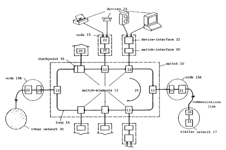
Referring to figure 1, the chosen network comprises
a packet-switch 10 consisting of a plurality of
switching elements 12 series-connected in a loop 14 of
suitable transmission media, each element 12 being
connected to a node 15. A check-point 16 is also
included in the loop, conveniently as an addition to one
of the switch elements 12, as shown.
Each node 15 comprises a switch interface 20 for
connection to the respective switch element 12 and a
device interface 22 which contains the node processor
and by which a variety of terminal devices 24 are
connected to the network. it is the function of switch
interface 20 to respectively packet and depacket data
fed to and from device interface 22, and the function of
device interface 22 to organize and feed data between
devices 24 and switch interface 20. The node processor
is a microprocessor which runs a resident windowing user
interface for handling multi-session communications,
protocol conversion routines for interfacing different
- 17 -
.
15768 CA
- 133~ 664
devices to the network, dataphone enhancements,
encryption services and the like.
In this example, switch 10 can accommodate 256
switch elements 12 (each with its node 15 and associated
terminal devices 24) including one checkpoint. The
switch elements are addressed by numbers progressing
sequentially around the loop from the checkpoint (which
is assigned the address of zero) with the direction of
data flow, as indicated by arrow 25. The address of a
switch element (and its node) is the loop address.
Not all nodes need be connected to terminal devices
such as digital telephones, host computers, computer
terminals, printers, plotters etc. The device interface
of node 15A is configured as a bridge to communicate
with a similar network 27 formed in accordance with the
present invention, while device interface of node 15B is
configured to communicate as a gateway to a dissimilar
network such as the public telephone system, an x.25
packet-switched network, an Ethernet (TM) or the like.
Such bridges and gateways perform address and, in the
case of gateways, protocol transformations between
networks in ways known in the art.
The format of the packets employed in this example
is shown in Figure 2. Block P depicts a packet of 176
bits comprising four fields: an 8 bit Type field T, an
eight bit Loop Address field LA, a 16 bit Socket number
field S and a 144 bit Data field D. The first two
fields form the packet header. Depending upon the
transmission media employed and the Data Link Layer
protocols, the packet may have a framing preamble A and
postamble B, but these are not required within a
compact, parallel-configured switch.
As shown by block T, the Type field itself
comprises five sub-fields designating, respectively, the
level of Priority of the service to be given to the
packet (2 bits), the quality of the service in terms of
Reliability (1 bit), a round trip (RTP) flat (1 bit), a
- 18 -
15768 CA
133~664
2 bit sub-field indicating how the socket address is to
be interpreted (viz: as a socket address (normal), as a
RQ_BCST, or BCST, and a Packet Type sub-field (2 bits)
indicating whether the Data field is to be interpreted
as memory, control, protocol or maintenance information;
the packet therefore being referred to accordingly as a
'Memory packet', 'Control packet' etc.
The Socket field S identifies a session buffer in
the address space of the node signified by the
associated Loop Address, and corresponds to a half-
session or simplex connection. There may, thus, be 64K
simultaneous full sessions active at one time at one
node, but one terminal device (such as a host computer)
may account for many sockets, and there may be many
devices connected to one node.
As shown by block M in Figure 2, when the Data
field is interpreted as memory information, the first 16
bits of this field will be read as a memory reference or
offset, and the remaining 128 bits as a 16 byte segment
of user data. It is this offset and its associated data
segment that are the subject of the DMT technique of
this invention. If the Data field is interpreted as
control information, the entire 144 bits will be taken
as an application-defined instruction to be passed to
the node processor for interpretation in accordance with
the communications or applications software running. if
the Data field is interpreted as protocol information,
the first 8 bits are used as a Command field and the
remainder indicate the protocol function concerned; for
example, a positive or negative acknowledgement (ACK or
NAK) of a packet, an end of block transfer (EOT), or a
request for status information (described below).
Finally, the Data field may be interpreted as network
management, maintenance and monitoring information.
One or more checksums may be incorporated in the
packet to provide greater security for one or more
- 19 -
15768 CA
- 1337661
fields in accordance with known techniques and are not
shown in this illustrative example.
The allocation of the two levels of priority will
not be described, being a known technique in register
insertion systems, and will be assumed to be offered
only in the 16 bit wide parallel version of the switch.
It is implemented (but not shown) in that version by the
use of two transmit FIFOs, one for high priority (voice)
and the other for low priority (computer data) packets.
Low-priority packets may be preempted from the hold FIFO
of a switch element to allow a packet in the high-
priority queue to be sent in its place, but the
preempted low-priority packet is, preferably assigned to
the high-priority queue.
The allocation of the two levels of reliability of
transmission is determined by whether the Data packets
have memory references or not. If so, the high-
reliability bit in the Type field is set and the
received packets are interpreted and acknowledged
accordingly; if not, that bit is not set and the whole
Data field is used for voice data which is handled in
small buffers at the receiving end using conventional
sliding window techniques.
In operation, data for transmission from, or
reception by, each terminal device 24 is exchanged with
device interface 22 under the control of an applications
program running on the interface processor which assigns
a socket number and buffer to each half-session (whether
receive or transmit). In the case of voice data
(digitized by known methods) the transmit socket may
only be 16 bytes (one packet data segment) while the
receive socket buffer for that connection may be a few
times greater (so that sequencing and delay compensation
can be performed by known methods using a small modulo).
The size of the socket buffer for voice communications
can be standard across the network and need not be
negotiated during call setup. In the case of computer
- 20 -
15768 CA
1337~64
data, the size of each of the four socket buffers
allocated to each connection (each end has a transmit
and receive socket) is negotiated at call set-up and
need not be symmetrical (though the socket buffers at
each end of the same half session will be of the same
size), can be as large as lMb, and can be dynamically
adjusted during a session through the exchange of
protocol, maintenance or control packets. Such
communications between sockets are thus virtual duplex
circuits.
The class (priority and reliability) of service to
be assigned to outgoing packets, together with their
loop and socket addresses and the base address of the
transmit socket buffer (in the case of Memory
packets)are assigned by the node software at call setup,
and are recorded in a transmission table (to be
described below with reference to Figure 13). The
switch interface 20 (a hardware device), is then able to
fetch successive 16 8-bit byte segments of data from the
appropriate location in each transmit buffer (in order
of assigned priority), to add the header and destination
socket number to each data segment to form a packet, and
pass the packets in turn to the associated switch
element 12. Switch element 12 then inserts the packets
into the loop 14 without contention or arbitration (as
described below).
The reception process is straight forward. Each
switch element recognizes packets addressed to it and
copies (or removes) them from the loop, stripping off
the loop address (if desired) and transferring them in
turn to the associated switch interface 20 where the
Type and Socket fields are read by the hardware. In the
case of Memory packets (which receive the high-
reliability service), the switch interface combines the
information in the incoming packet's Memory Reference
field with information contained in a receive session
table corresponding to the Socket Number field of the
- 21 -
15768 CA
1337~6~
packet, to generate a specific memory address in the
correct receive socket to which the 16 bytes of user
data should be transferred, and effect the transfer of
the data to that location. These actions implement the
direct memory transfer mechanism of this invention
without intervention of the processor at either of the
associated device interfaces 22 (apart from call set-up
and error recovery).
In the case of voice (typed as low-reliability) the
packets are passed by the switch interface 20 directly
to the appropriate socket buffers in the device
interface 22 where appropriate sequencing, delay
compensation and digital to analog algorithms are
applied. The re-constructed voice signal can then be
fed to the telephone terminal device corresponding to
the receive socket. Enroute, the high priority voice
packets will preempt the low priority computer data
packets at each switch element (as indicated above).
All other types of packets are also passed to the
device interface 22 by the switch interface 20, but they
are not directed into a socket buffer. Instead, they
will cause an interrupt on the device interface
processor and require some instruction to be serviced.
Figure lA illustrates the use of 'freeways' 14F in
the loop of the switch of Figure 1. Each freeway by-
passes a group of adjacent switch elements 12 on the
loop. The switch element at the start of a freeway
selects incoming packets that have higher addresses than
the address of the element at the exit of the freeway
and switch such packets onto the freeway. Broadcast
(and request to broadcast) packets are not routed on
freeways. If a freeway bypasses the checkpoint, then
the switch element at the start of the freeway must
perform the role of a checkpoint in relation to RTP
flags and, preferably in regard to the elimination of
corrupt packets.
15768 CA
The Serial Switch Element 133~ 66~
A distributed serial switch, in which the switch
elements and their associated nodes are geographically
5 spaced, is of value as a LAN system for a campus site.
A loop of this nature would be of value in linking high-
speed peripherals with a mainframe computer, for
example. Given suitable line drivers, modulators and
demodulators, any desired transmission medium may be
employed to link the switch elements. As is common in
such systems, the data is modulated on a continuous
carrier that provides a clock signal for each switch
element.
Referring to Figure 3, the serial switch element
15 12A is preceded on the loop by a conventional decoder 40
which provides the clock signal, detects the start of a
packet and decodes incoming packets. It is followed on
the loop 14 by encoder 42 which encodes the data for
serial transmission on the loop to the next switch
20 element. While the loop 14 itself is only one bit wide,
most other data paths in the serial switch element of
this example are the width of the packet header ( 16
bits).
The bit stream of every incoming packet is fed from
internal loop section 14A via line 43 into a 16 bit
series-to-parallel receive register 44 so that the loop
address and type fields can be read by a control logic
unit 46 via input bus 48, and so that each word of
packets addressed to the switch element can be shifted
via bus 50 into receive FIFO 52 and via output bus 54 to
the associated switch interface. The bit stream of each
packet is also presented via loop section 14A to an
output multiplexer 56 so that, if that data stream is
selected, it will flow straight through the switch
35 element to encoder 42 and onto loop 14 again. An
isolating flip-flop 58 is interposed in the loop between
multiplexer 56 and encoder 42 to provide a one bit
,
15768 CA
-- 1337664
buffer to mask switching transients in multiplexer 50.
Multiplexer 50 normally is set to select data on the
internal section 14A of the loop. Finally, the input
bit stream is also presented via line 60 to a one-bit-
wide, variable-length hold FIFO 62 from which it can be
shifted to a second input 64 into multiplexer 56.
Control logic unit 46 can over-write the first 16 bits
of hold FIFO via bus.
On the transmit side of the switch element, packets
for transmission are shifted into the transmit FIFO 68
via bus 70 from the associated switch interface. From
the transmit FIFO 16 the packets can be shifted out in
16 bit words via bus 72 to a parallel-to-series transmit
register 74 and from there as a serial bit stream to a
third input to multiplexer 56 via line 76.
The operation of the serial switch element of
Figure 3 will now be described.
With receive FIFO 52 and transmit FIFO 68 empty and
multiplexer 56 in its normal state, the bits of an
incoming packet stream into receive register 44, into
hold FIFO 62 and through multiplexer 56 onto the loop
again with only one bit delay. After the first 16 bits
have been clocked in, the packet header in receive
register 44 is read by logic unit 46. If an incoming
packet is addressed to 'this address', or has its
broadcast flag set, logic unit 46 shifts successive
words of the packet as they fill receive register 44
into receive FIFO 58 and from there to the switch
interface. In the meantime, however, the bits of the
original packet have been streaming through multiplexer
56 from the loop section 14A and are proceeding to the
next switch element on the loop as a 'dead' packet
(unless it is a broadcast).
A packet which is not broadcast, is addressed to an
earlier (upstream) node and or does not have its RTP
flag set, it is said to be dead. A switch element which
allows incoming packets to flow straight through on the
- 24 -
15768 CA
l337~64
loop is said to be 'non-buffering'; one in which
multiplexer 56 is switched to block the loop is said to
be 'buffering'.
Should the receive FIFO 52 be full when the header
of an incoming packet with 'this address' (or a
broadcast) is clocked into receive register 44 (and when
the switch element is non-buffering) it will be too late
to set the RTP flag in the original packet in transit on
the loop which will, again proceed as a dead packet.
Instead, hold FIFO 62 is allowed (by logic unit 46) to
expand to accommodate all the bits of the incoming
packet. The header of the packet will be clocked into
both the receive register 44 and the first 16 bits of
the hold FIFO at the same time so that the control logic
46 can recognize the address and set the RTP flag (and
insert 'this address' in the case of a broadcast) in the
packet header held in the hold FIFO 62. When the change
has been made, and after the original packet has left
multiplexer 56, the control logic 46 switches
multiplexer 56 to select line 64 and proceeds to shift-
out the modified packet from hold FIFO 62, shrinking
that FIFO accordingly.
Should another packet arrive while the modified
packet is proceeding in this way, its passage on loop
14A will be blocked by multiplexer 56, but it will be
clocked into hold FIFO immediately behind the last bit
of the first packet and its header will be read by the
logic unit 46 after being clocked into receive register
44. If it is also for 'this address' and receive FIFO
is still full, it will be shifted into the hold FIFO 62
until its header reaches the end (when control logic
stops shifting the packet in) and its header will be
modified as before and it will be put back on the loop
as before.
If the switch element is buffering, and an incoming
packet is a dead packet, hold FIFO will not be expanded
to accommodate it and successive bits will be overwrite
- 25 -
15768 CA
1337664
-
one another in receive register 44, thereby destroying
the packet. If, however, it is a valid packet addressed
to a down-stream element, it will be buffered by hold
FIFO 62 and put on the loop (without modification)
immediately after the preceding packet from FIFO 62.
With the switch element in the non-buffering state
and a packet in transmit FIFO 68 for transmission, logic
unit 46 switches multiplexer 56 to select line 76 (thus
changing switch element to its buffering state) and the
packet in transmit FIFO 68 is parallel-shifted word-by-
word through transmit register 82 and then series-
shifted onto the loop 14. Any packet arriving while
this is taking place is handled as described above for
the buffering switch element.
Broadcasts (BCSTs are handled as indicated earlier.
A non-buffering switch element will transfer broadcast
packets straight onto the exit loop unchanged (to be
read by all other switch elements), but upon recognizing
a BCST, control logic will shift it into the receive
FIFO for transfer to the switch interface. If the
switch element is buffering, the BCST packet will be
shifted into the receive FIFO 52 as before, but it will
be held by hold FIFO 62 until the packet in transit from
transmit register 74 has departed, after which
multiplexer 56 will select line 64 and the delayed BCST
will be put back on the loop.
If, however, the switch element is buffering and
the receive FIFO 52 is full, control logic 46 will
change the packet header (held in hold FIFO 62) into a
RQBCST and the address into 'this address'. This
packet will proceed as a valid packet passed the
checkpoint 16 on the loop where it will not be read by
earlier elements (because of its non-zero address) unit
it reaches the original switch element which will
recognize its own address. At that point (if the
element is non-buffering) the packet will (i) proceed on
the loop to be removed by the checkpoint (not having
- 26 -
~ ~,
15768 CA
t 337~A
been read by other elements), (ii) be copied and shifted
into the receive FIFO 52, and (iii) be held in the hold
FIFO 62 while control logic changes it back to a regular
BCST with the address of the checkpoint (zero) and then
put back on the loop.
Any switch element wishing to initiate a BCST,
issues a RQ_BCST packet addressed to the checkpoint,
where the RQ_BCST flag is changed to a BCST flag and the
packet put back on the loop.
Finally, it should be noted that the direct line
(14A) through the switch element was included in the
example to minimize delay in the non-buffering element.
Without this, the switch element would work
substantially as described but every packet would be
delayed in the hold FIFO 62 long enough for the control
logic to read enough of the header to make and effect a
decision. This may be of no consequence on high speed
loops with very short bit times, but is undesirable on
loops with, say, twisted-pair media.
The Checkpoint
The checkpoint 16 (Figure 1) for the serial switch
is practically identical in design to the switch element
just described. The most important difference is that
its control logic ensures that it always buffers a whole
packet so that the control logic can detect and
eliminate a corrupt packet.
The basic function of the checkpoint is to remove
all packets which do not have a RTP flag set, to remove
any RTP flag in a packet, to convert all RQ_BCSTs
(requests to broadcast) to BCSTs (broadcast) and remove
all dead packets from the loop. As before, the removal
of packets is simply accomplished by not shifting them
out of the hold FIFO and letting succeeding packets
over-write them. One of the devices which may be
- 27 -
,
-
15768 CA
1337664
connected to a checkpoint switch element is a network
manager's console which allows a network manager to
initiate broadcasts, regulate the rate of transmission
from individual nodes, compute billings and generally
monitor the system through the use of Maintenance and
Control packets. To regulate the rate of transmission
from switch elements, for example, each element would
include a re-settable status counter to count packets
passing through the transmit FIFO, and a re-settable
control register accessible only to Control packets sent
by the loop manager. (The status counter could also be
directly interrogated by the loop manager for billing
purposes.) The counters are compared from time to time
and transmission of packets stopped when the status
count is equal to that of the control register setting.
The rate of transmission can thus be set by periodically
resetting the status counter and adjusting the entry in
the status register.
The 16-bit Parallel Switch Element
For high speed packet-switching and data
transmission, some degree of parallelism is required in
the loop media and packet switches formed in accordance
with this invention can have any desired degree of
parallelism up to the number of bits in a packet. The
preferred minimum for a parallel loop system is,
however, 16 as this is the number of bits in the header
of the packet described above and it is a sum-multiple
of the number of bits in the packet. A switch of this
type will be a compact item of equipment and may even be
implemented as a VLSI chip. A switch element for such a
switch is described below with reference to Figure 4.
The 16 bit bus which comprises the loop 100 enters
the switch element 12B and serially transits an input
register 102, a variable-length hold FIFO 104 and a
multiplexer 106, but before leaving the switch element,
- 28 -
15768 CA
- 133766~
,
it passes through an output stage 108. Encoders and
decoders are not needed in this version of the switch as
the switch elements are in very close proximity to one
another. After input register 102, bus connections from
the loop 100 are taken, (i) through a 2-cycle delay
element 110 (via bus 111) and receive FIFO 112 to the
switch interface via bus 114, and (ii), to an address
comparator 116, error checker 118 and the control logic
unit 120.
The control logic unit 120 will have many
connections (indicated by arrows 121) to and from the
other circuits in the switch element. These will be
explained below, but are not shown for the sake of
simplicity. The reason for the two output busses 100a
and 100b from hold FIFO 104 to multiplexer 106 will also
be explained below.
On the transmit side, packets receive from the
switch interface (in 16 bit words) are transferred via
bus 122 to transmit FIFO 124 and from that FIFO to the
- 20 multiplexer 106 via bus 126. Finally, an error check
generator 128 receives the loop output from the switch
element via bus 132 and computes a checksum which is
then presented on bus 130 as another input to the
multiplexer 106.
A convenient board-level implementation for such a
switch is to run the loop and other common connections
for the switch elements on a backplane into which each
switch element board is plugged. In addition to the
loop bus, the other data lines carried by such a
backplane will include a 16 bit bus 134 (which sets the
switch element address according to the backplane socket
used), and a first-word-in line 136 which is daisy-
chained from switch element to switch element and
signals when the first word of a packet is valid in
input register 102. Thus, the control logic generates a
first-word-out signal on line 138 which comprises the
signal for the first-word-in line of the next element in
- 29 -
15768 CA
133766 1
the loop. Other backplane connections (not shown) will
include, a 'hard' reset line, a clock line (25 Mhz) and
power lines. This implementation assumes that the
switch element and its associated switch interface are
in close proximity, possibly on the same circuit board.
In operation, a packet word is clocked from one
switch element to the next each clock cycle (giving the
nominal rate of date transfer between switch elements of
400 Mhz). When the first word of a packet is valid in
receive register 102 ( as signalled on line 136), its
address is compared with the address of this switch
element in comparator 116 and control logic is signalled
as to whether the packet address is greater or less than
this address and whether it is zero, and it header is
checked by circuit 118 and the control logic is
signalled if there is an error.
Control logic 120 then routes the packet (by
shifting successive words) in accordance with the
principles described for the serial switch element of
Figure 3. That is: if the packet is valid and for 'this
address' it is shifted into receive FIFO via the 2-bit
delay 110 (included for ease of timing) and any packet
waiting in FIFO 124 is shifted through multiplexer 106
onto loop 100; if it is dead, the first (and all later
words are not shifted out of input register 102 and a
waiting packet in transmit FIFO 124 can again be
transmitted; if the packet is valid but not addressed
'here', and if no packet is waiting in transmit FIFO 124
and the hold FIFO 104 is empty, the incoming packet is
shifted (with a one word delay) through hold FIFO 104
and multiplexer 106 onto the loop 100; if an output
packet (from FIFO 124) is in transit through multiplexer
106, the incoming packet is shifted into hold FIFO 104
(which expands as needed); and, if the receive FIFO is
full, any incoming packet for 'this address' is stepped
through hold FIFO 104 (being buffered as necessary) and
into output stage where its header is modified
- 30 -
15768 CA
1337664
appropriately. (The input LA into output stage 108
indicates that the loop address for this switch element
is fed to that circuit so that it can be selected by the
control logic 120 if it is needed in the case of a
RQ_BCST.)
The operation of the switch element of this example
is also described by the Model Programs of Appendix 1
appended hereto and suitable chips for use in the
circuit are listed in Appendix 2 so that those skilled
in the art will be able to design and build a switch
element to operate as described. However, further
comment on some of the functional circuits is provided
below.
Referring to Figure 5, the hold FIFO 104 can be
conveniently implemented using available 16 bit
multilevel pipeline registers (MPRs) having a variable
delay of between one and four cycles. Three Mars (MPR1,
MPR2 and MPR3) are used in series to give a total delay
of 1 - 12 cycles (the packet being 12, 16 bit words in
length). Input bus 100 to the hold FIFO is the input to
MPR1, while output bus lOOa from the FIFO is the output
of a series transition of all three Mars and output bus
lOOb is the output of the transition of only the first
MPR. Control lines 150 (two for each MPR) are for the
control signals from the logic unit 120. A 1 - 4 cycle
delay is effected by the control of MPR1 and selection
of bus lOOb by multiplexer 106, while a 5 - 12 cycle
delay is effected by control of all three MPRs and the
selection of bus lOOa.
Figure 6 illustrates the way in which the receive
and transmit FIFOs may be constructed. The complication
is that the logic unit 120 needs inputs signifying that
each of these FIFOs are empty or full, meaning that they
contain no packets or that no more (whole) packets can
be fitted into them, but FIFOs constructed in the normal
way from dual-port random access chips will only
15768 CA
133~66A
indicate empty when they contain no words and full when
no more words can be fitted in. The operation of the
receive FIFO 112 will be described, but transmit FIFO
124 can be identical. Input bus 111 feds the dual port
random access memory unit 152 and output bus 114 leaves
it and, also in the conventional way, unit 152 is
controlled by a write address counter 154 and a read
address counter 156 via respective write and read buses
158 and 160.
To maintain a packet count, an up/down counter 162
and a comparator 164 are employed as shown. Counter 162
receives count-up signals on line 166 and count down
signals on line 168 from respective write complete and
read complete signals derived from the counter 154 and
counter 156 respectively. The running difference
(representing the number of packets in RAM 152) is
indicated on bus 170 to the comparator 164, which is set
to provide a 'FIFO full' signal on line 172 and a 'FIFO
empty' signal on line 174 when the count on line 170 is
greater than 46 and less than one respectively. These
signal lines are connected to the logic unit 120.
Figure 7 illustrates a suitable circuit for the
address comparator 116, the inputs to which are 'this'
loop address on 8 bit bus 134 and the loop address of
the incoming packet (when its header is valid in input
register 102), also an 8 bit bus. These two inputs are
received by a magnitude comparator 182 which provides
two output signals, one on line 184 when the loop
address is greater than 'this address' and one on line
186 when the loop address is less than 'this address',
both signals being fed to the logic unit 120. Finally,
the address of the incoming packet on line 180 is fed to
a NOR gate 188 which provides an output on line 190 when
the input address is zero.
The error checker 118 (Figure 8) receives the
entire header field on bus 192 from the input register
(when the first word of a packet is valid therein).
- 32 -
15768 CA
- 13~7664
This is fed to one input of an exclusive OR gate 194,
the output of which is fed to a register 196, in turn,
is connected to the second input of gate 194 via
feedback loop. Output of gate 194 is then fed to an OR
gate 202 via bus 203. In operation, the register 196 is
initialized by the recording of a checksum via control
line 204. When a packet header is received it is XOR'd
with the checksum and, if the result is not zero on all
lines of bus 203, an error is produced on signal line
206 to the control logic unit 120.
The function of the error check generator (see
Figure 9) is two-fold: first, to compute a checksum
after reading (via bus 130) all the bits of each
successive word of a packet leaving the switch element
on bus 100, and to write that checksum (via bus 132 and
multiplexer 106 in Figure 4) into the postamble of the
packet; and, second, to place a corrupt checksum into
any packet found to be corrupt by error checker 118 so
as to ensure that any change made to the header in the
next switch element does not, by chance, make the
checksum correct. Referring to Figure 9, it will be
seen that an OR gate 210 and register 212 are connected
as in the error checker of Figure 8 and that there is no
or gate in output bus 132. Instead, one of the lines
from bus 132 is XOR'd by gate 214 with the signal on
line 206 from error checker 118. This effects the
corruption of the checksum generated.
Figure 10 provides a detail of output stage 108,
the function of which is to insert 'this address' in any
RQ_BCST via 8 bit bus 134a and to insert any
modifications to the 8 bit Type field via 8 bit bus 230
from the control unit 120. Bus 134a and bus 230 are
presented as input to respective multiplexers 238 and
240, which also each receive the corresponding half (8
bits) of the 16 bit loop bus 100, the respective 8 bit
buses from multiplexers 238 and 240 being combined to
form the 16 bit loop bus 100 which is fed to an
15768 CA 13 ~ 7 6 64
-
isolating register 242 before leaving output stage 108
and the switch element. In operation, when the first
word of a packet is clocked from multiplexer 106 on the
loop bus, control logic unit 120 switches multiplexers
238 and 240 to select the appropriate inputs to create a
modified header, or to leave it unmodified; there-after
and for the remainder of the packet, the multiplexers
are switched to their normal conditions which is to
select the two loop bus inputs.
Finally, freeways may be implemented in parallel
forms of the switch element and, in view of the lack of
geographic constraints and the much higher capacity of
parallel swltches, the use of freeways is likely to
confer greater benefits in the parallel configuration of
the switch and loop. Figure 11 (in conjunction with
Figure lA) indicates how the 16 bit switch element of
Figure 4 can be readily modified to provide for inputs
and outputs to freeways, like parts in both Figures
being numbered the same. As will be seen, an input
freeway 250 can simply enter the switch element as
another input to multiplexer 106, being selected by the
control unit 120 (not shown in Figure 11) when, (i) a
valid packet header is presented in register 102 with an
address greater than that at the end of output freeway
252, and (ii) when control unit 120 receives a signal
indicating that multiplexer 106 at the other end of
freeway 525 is not switched to another input and that
the other switch element is not in the buffering state.
Should either of these conditions occur, the packet (the
header of which is in register 102) will be routed as
normal.
The Switch Interface and Direct Memory Transfer
The switch interface 20 and its connections to the
device interface 22 (see Figure 1) is shown in detail in
Figure 12 and its logical operations are
- 34 -
,~
i_~
1~768 CA
1337664
diagrammatically shown in Figure 13. It should be
noted, however, that Figure 12 is a diagram of the
essential hardware components for both the transmit and
receive side of one switch interface, while the logical
operations of Figure 13 assume a virtual connection (via
packets on the network) between the transmit side of the
switch interface associated with one switch element and
the receive side of another switch interface associated
with the input side of another switch element. It
should also be noted that the packets presented to the
switch interface in this example are truncated; that is
they are without their loop address field, this
information having already been used.
Referring to Figure 12, packets from the receive
FIFO of the associated switch element 12 or 12b are
shifted (word by word) into the associated switch
interface 20 via bus 54 and distributed to a control
packet FIFO 300 via bus 302, a socket register 304 via
bus 306, an offset register via bus 310, and to an
output bus interface unit 311 via bus 312. Socket
register 304 and offset register 308 respectively latch-
in the socket address and the offset fields of each
incoming packet, the socket number being used to index a
receive session table 312 via bus 314 and the offset
being passed by bus 316 to adder 318 which adds the base
address on bus 320 (corresponding to the indexed socket
number) read from table 312 and presents the sum as a
memory address to output bus interface unit 312 via 24
bit bus 322.
Also read out (via bus 324) from the session table
is the address for the expected end of the block for
that session number which is sent to the bus interface
unit 312 on bus 322, and used in the limit check circuit
326. Upon the receipt of an end-of-block packet is
received from the transmit end with its checksum, the
two checksums are compared and, a signal is sent to an
15768 CA
766 1
output scheduler 328 via a control line (not shown)
indicating that an end of block ACK (or NAK) packet
should be queued in the scheduler for transmission, the
relevant receive socket number for that session being
provided by socket register via bus 330. As each word
of each packet of a block is transferred to bus
interface 312 on line 314, its bits are employed in the
running computation of a block checksum and, at the end
of the block, the final computed checksum is compared
with that read out from the receive session table 302.
This process is indicated by the + symbol at 332 and
busses 334 and 336. It is this computation that
determines whether an ACK or a NAK is sent at the end of
a block transmission.
The bus interface unit and the control packet
receive FIFO are connected to processor bus of the
device interface 20, the processor and its memory being
generally indicated at 342 and 344. Each control packet
in FIFO 300 causes an interrupt to the processor, but
the interface unit 312 is able to write data direct to
memory 344 without requiring processor intervention.
The session buffers are sections of memory 344.
On the transmit side, a second bus interface unit
346 also interacts with the processor bus 340 and memory
344 without generating interrupts; it places a read
address on the bus 340 (via bus 348) and accepts the
data read from memory 344 via bus 350. The data (in
successive words for inclusion in an outgoing Memory
packet) is presented to multiplexer 352 (via bus 354) by
the action of which packets are assembled and forwarded
(as a series of 11 words) to the transmit FIFO of the
switch element 12 or 12A. The other inputs to
multiplexer 352 are: bus 356 from a FIFO 358 for control
packets (loaded therein from bus 340 via bus 360 under
programmed control of processor); the offset field data
derived via bus 362 from a transmit session table 364;
the block checksum, also derived from table 364, via bus
15768 CA
1337664
366; and the loop address on bus 368 for the outgoing
packet, also derived from the table 364.
As shown symbolically by the plus sign at 370, the
block checksum is built from inputs from the data bus
354, the offset bus 362 and the accumulated or running
checksum from table 364 via bus 372. With each word
transmitted, the offset derived form table 364 via bus
362 is incremented; this is indicated symbolically at
374. The count of the remaining words to be sent in the
block is decremented each time a word is sent and that
is symbolically indicated at 376. Finally, the address
from which the original data was read in memory 344 is
generated by adder 378, which receives the base address
from the session table 364 (via bus 380) and the offset
(from bus 362) and transmits the result on bus 382.
Referring to Figure 13 which illustrates the above
process in a different way, the data flow is from left
to right; from the read address (bus 322) and data (bus
354) at the source and using the transmit session table
364 to build the packet P (which transits the network),
to the memory write address (bus 322) using the receive
session table 313.
On the transmit side, as will be seen from Figure
13, the socket number (on bus 329 from scheduler 328,
Figure 1) indexes transmit session table 364, providing
the base address, the offset, block length, destination
address (including type, loop address and socket number)
to be entered into each packet; the 11 words of data
associated with that packet being provided on bus 354.
The data in (the whole of) each packet is used to build
the transmit block checksum as indicated. The offset
for each packet is computed by incrementation as shown
at 386 and, together with the base address (as shown at
388), furnishes the read memory address on bus 322 for
the data on bus 354 for that packet. As each packet is
despatched, the block length still remaining is
decremented, as indicated at 390.
- 37 -
15768 CA
1337664
On the transmit side, the block checksum is
accumulated from the data for each packet and up-dated
in the table 364 each packet, as shown at 392. It is
preferable, as shown by the dotted line 394, to include
the offset field in the checksum so that there will
always be a varying quantity in the accumulating block
checksum, even if the data is constant.
On the receiver side, the session number field
(derived from the packet) on bus 306 again indexes the
table giving the base address, the block limit,
accumulated block checksum, and the remaining block
length. The valid session field is included to allow
data to spurious addresses to be discarded.
The memory reference or offset on bus 310 is added
to the base address (as indicated at 396) to furnish the
write address on bus 322 to the memory in the device
interface. The 8 words of data contained in the packet
are transferred on bus 312 to the address signified on
bus 322, and also contribute to the running block
checksum calculated (as shown at 397). The offset is
used, as before, as an input to the block checksum
calculation (as indicated by dotted line 398), and also
as a means of checking to see that the block limit has
not been exceeded (as shown at 400). Finally, the
number of packets received (or the length of the data
accumulated data block) is incremented for each packet
as shown at 401.
- 38 -
1337ii 6A
INDUSTRIAL APPLICABILITY
The industrial applicability of this invention and its
embodiments has already been indicated. However, it
will be appreciated by those skilled in the art that
there will be many different ways in which this
invention may be applied in practice without departing
from the principles disclosed or claimed in the
following claims. For example, a half-parallel (92 bit)
switch using the packets described and running on a 30
nano second cycle time (33.3 Mhz) would have a data
transfer capacity of 3.2 Gb/s. It will also be seen
that the direct memory transfer principle need not be
used only with the improved switch, or vise versa,
though only the combination will yield the full benefits
and advantages disclosed herein.
- 38a -
15768 CA
- 1337~6A
REFERENCES
* Ahuja, V, "Design and Analysis for Computer
Communication Network" Mc Graw-Hill, 1985
* Bridges, C P, "Low Cost Local Area Networks"
(Halstead Press, NY 1986)
* Farmer, W D, and E E Newhall, "An Experimental
Distributed Switching System To Handle Bursty
Computer Traffic". Proc. ACM Symp. Problems
Optimization Data Comm. Systems, Pine Mountain
Georgia, Oct. 1969.
* Hafner, "A Digital Loop Communication System" (IEEE
Transactions on Communications, Vol COM-22 No. 6,
June 1974)
15 * Hayes et al, "Traffic Analysis of a Ring Switched
Data Transmission System" (Bell System Technical
Journal, Vol 50, No 9 Nov. 1971; pp 2947 - 2978)
* Majithia et al, "Analysis and Simulation of Message
Switched Loop Data Networks" (Proc. IEE Vol 124, No
3 March 1977)
* Reames, C C, and M T Liu, "A Loop Network For
Simultaneous Transmission of Variable Length
Messages". Proc. Ann. sYmp. Comput. Architecture,
2nd Jan 1975.
25 * Reames C C, and M T Liu in, "Design And Simulation
of The Distributed Loop Computer Network (DLCN)".
Proc. Ann. Symp. Comput. Architecture 3 Jan. 1976.)
* Shiva, S G, "Computer Design and Architecture",
Little, Brown and Cp., 1985
30 * Tanenbaum, A S, in "Computer Networks" (Prentice
Hall, 1981).
* Tropper, C, "Local Computer Network Technologies",
Academic Press, 1981
- 39 -
15768 CA
13376~4
Appendix 1-1
MODEL PROGRAMS
5 Program 1 Transfer of data from the switch-element ot the switch-interface.
DO-FOREVER
BEGIN
IF ( receive-FIFO not empty ) DO
BEGIN
data-available := TRUE;
WITH words one to eleven of each packet from the receive-FIFO DO
BEGIN
receive-data := current word of the packet;
WAIT-UNITL read is TRUE;
END
decrease the count of packet in the receive-FIFO by one;
END
data-available := FALSE;
END
Program 2 Transfer of data from the switch-interface to the switch-element.
DO-FOREVER
2 5 BEGIN
transmit-FIFO-full := FALSE;
WITH words one through eleven of the packet DO
BEGIN
WAIT-UNTIL write is TRUE;
store the word available on transmit-data into th transmit-FIFO;
END
transmit-FIFO-empty:= FALSE;
increase the count of packet in the transmit-FIFO by one;
IF ( transmit-FIFO full ) DO
3 5 BEGIN
transmit-FIFO-full := TRUE;
WAIT-UNTIL transmit-FIFO not full
- 40 -
15768 CA
-
Appendix 1-2 1 3 3 7 6 6 4
END
END
Program 3 Transfer data from the loop input bus to the appropriate
destination within the switch-element. NOTE: the variables 'new-type-
field', 'new-loop-address' and 'bad-checksum' are used to communicate with
the following algorithm.
DO_FOREVER
BEGIN
IF ( first word of packet available on loop-input-port ) DO
BEGIN
new-type-field := type-field;
new-loop-address := loop-address;
bad-checksum := falsei
IF ( loop-address EQUAL this-address AND
type-field.round-trip-flag EQUAL O AND
type-field.address-type EQUAL normal ) DO
Non-Broadcast Packet addressed to us.
}
BEGIN
IF ( receive-FIFO-full ) DO
{
30 Receive-FIFO-full, pass packet back around the loop.
}
BEGIN
new-type-field.round-trip-flag := l;
WITH words one to twelve of the incoming packet DO
BEGIN
place next word into hold-FIFO;
END
IF ( calculated checksum NOT_EQUAL checksum ) DO
BEGIN
- 41 -
15768 CA
1337664
Appendix 1-3
bad-checksum := true;
END
END
ELSE
Receive-FIFO has room, place incoming packet into the receive-FIFO.
}
BEGIN
WITH words one to eleven of the incoming packet DO
BEGIN
place next word into the receive-FIFO;
1 5 END
IF ( calculated checksum NOT_EQUAL checksum ) DO
BEGIN
clear last eleven words from receive-FIFO;
END
2 0 discard word twelve of incoming packet
END
END
ELSE IF ( loop-address EQUAL O AND
type-field.round-trip-flag EQUAL O AND
type-field.address-type EQUAL broadcast ) DO
{
Broadcast Packet.
}
BEGIN
IF ( receive-FIFO-full ) DO
{
Receive-FIFO full, convert packet to broadcast-request and pass
back around loop.
}
BEGIN
new-type-field.address-type := broadcast-request;
new-loop-address := this-address;
- 42 -
15768 CA
- 1337664
Appendix 1-4
new-type-field.round-trip-flag := 1;
WITH words on to twelve of the incoming packet DO
BEGIN
place next word into hold-FIFO;
END
IF ( calculated checksum NOT_EQUAL checksum ) DO
BEGIN
bad-checksum := true;
END
END
ELSE
15 {
Room in receive-FIFO for broadcast packet. Receive it AND pass
it on to the next switch-element in the loop.
BEGIN
WITH words one to eleven of the incoming packet DO
BEGIN
place next word into the receive-FIFO;
place next word into hold-FIFO;
END
place twelfth word in hold-FIFoi
IF ( calculated checksum NOT_EQUAL checksum ) DO
BEGIN
clear last eleven words from receive-FIFO;
bad-checksum := true
END
END
END
ELSE IF ( loop-address EQUAL this-address AND
type-field.round-trip-flag EQUAL O AND
type-field.address-type EQUAL broadcast-request ) DO
{
- 43 -
15768 CA
13~37~i64
Appendix 1-5
Request to Broadcast Packet.
}
BEGIN
IF ( receive-FIFO-full ) DO
{
Receive-FIFO is full. Pass Packet back around the loop.
}
BEGIN
new-type-field.round-trip-flag := 1;
WITH words one to twelve of the incoming packet DO
BEGIN
place next word into hold-FIFO;
END
IF ( calculated checksum NOT_EQUAL checksum ) DO
BEGIN
bad-checksum := true;
2 0 END
END
ELSE
{
Room in receive-FIFO to receive packet. Receive it and pass it
on to next switch-element in loop, converting it back into a
broadcast packet.
}
BEGIN
new-type-field.address-type :=broadcast;
new-loop-address := O;
WITH words one to eleven of the incoming packet DO
BEGIN
place next word into the receive-FIFO;
place next word into hold-FIFO;
END
place twelfth word in hold-FIFO;
- 44 -
15768 CA
- 1337664
Appendix 1- 6
IF ( calculated checksum NOT_EQUAL checksum ) DO
BEGIN
clear last eleven words from receive-FIFO;
bad-checksum := true;
END
END
END
END
END
Program 4 Transfer of data from either the hold-FIFO or transmit-FIFO
15 onto the loop output bus. NOTE: the variables 'new-type-field', 'new-
loop-address' and 'bad-checksum' are used to communicate with the
previous algorithm.
DO-FOREVER
BEGIN
IF ( hold-FIFO not empty ) DO
BEGIN
WITH word one from the hold-FIFO DO
BEGIN
loop-output-port := new-type-field OR new-loop-address;
END
WITH words two to eleven from the hold-FIFO DO
BEGIN
loop-output-port := word from hold-FIFO;
END
corrupt-checksum := bad-checksum;
loop-output-port := generated-checksum;
END
ELSE IF ( transmit-FIFO not empty ) DO
3 5 BEGIN
WITH word one from the transmit-FIFO DO
BEGIN
IF ( loop-address GREATER_THAN this-address ) DO
BEGIN
- 45 -
15768 CA
133~ 66A
Appendix 1-7
type-field.round-trip-flag := O;
END
ELSE
BEGIN
type-field.round-trip-flag := 1;
END
loop-output-port := type-field OR loop-address;
END
WITH words two to eleven from the transmit-FIFO DO
BEGIN
loop-output-port := word from transmit-FIFO;
END
corrupt-checksum := false;
loop-output-port := generated-checksum;
END
END
- 46 -
15768 CA
1337664
Appendix 2-1
REco~M~nED PARTS
FOR FIGURE 5.
Comp. Name Reference No. Part No. Quantity Manuf. Ref.
MPRl Am29521 2 AMD
MPR2 Am29521 2 AMD
MPR3 AM29521 2 AMD
FOR FIGURE 6.
Comp. Name Reference No. Part No. Quantity Manuf. Ref.
Address Counter 154 74F161 3 Fairchild
Address Counter 156 74F161 3 Fairchild
Dual-port ram 152 74F399 3 Fairchild
Dual-port ram 152 CY7C123 8 Cypress
Up/Down counter 162 74F192 2 Fairchild
Comparator 164 74AS885 1 TI-LSI
Comparator 164 Am25LS2521 1 AMD
FOR FIGURE 7.
Comp. Name Reference No. Part No.Quantity Manuf. Ref.
Comparator 182 74AS885 1 TI-LSI
Nor-gate 188 74S260 1 TI
Nor-gate 188 74F08 1/4 Fairchild
FOR FIGURE 8.
Comp. Name Reference No. Part No. Quantity Manuf. Ref.
Xor-gate 194 74F86 4 Fairchild
Register 196 74F374 2 Fairchild
Or-gate 188 74S260 1~ TI
Or-gate 188 74F20 1/2 Fairchild
- 47 -
15768 CA
1337664
Appendix 2-2
FOR FIGURE 9.
Comp. Name Reference No. Part No. Quantity Manuf. Ref.
Xor-gate 210 74F86 4 Fairchild
Xor-gate 214 74F86 1/4 Fairchild
Register 196 74F374 2 Fairchild
KEY TO MANUFACTURER REF.
Manufacturer Ref. Book
AMD Advanced Micros Devices
Bipolar Microprocessor
Logic and Interface 1985
Fairchild Fairchild
Fast Data Book 1985
TI Texas Instruments
The TTL Data Book
Volume 2 1985
TI-LSI Texas Instruments
LSI Logic Data Book 1986
Cypress Cypress Semiconductor
Cmos Data Book 1987
- 48 -