Note: Descriptions are shown in the official language in which they were submitted.
1 338068
.
1 TITLE OF THE INVENTION
Image Processing Apparatus
BACKGROUND OF THE INVENTION
Field of the Invention
The present invention relates to an image
processing apparatus, and more particularly to an
image processing apparatus capable of synthesizing
plural images.
Related Background Art
There are already known image synthesizing
apparatus for preparing an image by synthesizing
plural images.
Among such apparatus, there is for example
known one, disclosed in the U.S. Patent No. 4,320,962
of the present assignee, for storing two original
images in two memories and synthesizing said two
images by displacing the timing of image signal reading
from said two memories. There have also been various
proposals on image synthesis, such as those disclosed
in the U.S.Patent No. 4,417,805.
However such apparatus are only capable of
reading and synthesizing original images, and are
unable to effect synthesis with images other than such
original image.
There is also known a digital copying machine
~,
1 338068
-- 2
1 capable of trimming a predetermined position of an
original image for example with a digitizer, and
copying the image only of thus trimmed image.
However, in synthesizing video signal supplied
S from the outside in such copying machine, there is
required a complex structure for designating the
synthesizing position of said video signal, separately
from the trimming function of said copying machine.
Also there is already known a recording
apparatus having a page memory capable of storing input
image data of at least a frame, and capable of
producing plural prints of same image based on image
data read from said page memory.
In such apparatus there may occur jamming of
printing sheets or lack of printing sheets in the
course of printing plural sheets.
In order to rectify such situation, the present
applicant already proposed a technology of not
repeating the data writing into the page memory but
automatically continuing the printing of plural sheets
after such error state is resolved.
However such apparatus is often inconvenient
for use, since the printing operation of plural sheets
is automatically continued when the error state is
resolved.
More specifically, when the operator resolves
the error state, the printing operation is executed
- 3 - l 33 8 0 6 8
immediately without any other actuation. Such situation
is different from the ordinary printing operation and may
be misunderstood as an error operation by the operator.
Furthermore, if the aforementioned page memory is
composed of a memory device requiring refreshing
operation at a predetermined interval, such as a DRAM,
synchronization signals for said refreshing operation are
obtained for example from a clock generator to retain the
internally stored information.
However if the reference signals generated for
refreshing operation of the DRAM are switched to other
non-synchronized signals for some reason, the refreshing
interval may be prolongated before or after said
switching, whereby the stored information may become
unstable and eventually destructed.
SUMMARY OF THE INVENTION
A first object of the present invention is to
provide an improvement on the aforementioned image
processing apparatus.
Another object of the present invention is to
provide an apparatus capable of securely protecting
stored information.
~ 4 ~ 1 3 3 8 068
The foregoing objects can be achieved, according
to an embodiment of the present invention, by an image
processing apparatus comprising: (a) a memory requiring
refreshing operation at a predetermined interval; (b) a
first synchronization system for generating
synchronization signals for said refreshing operation;
(c) a second synchronization system not synchronized with
said first synchronization system; and (d) control means
for prohibiting the refreshing operation in a cycle
lo longer than said predetermined interval at the switching
of said first and second synchronization system.
Further objects of the present invention, and the
advantages thereof, will become fully apparent from the
following description to be taken in conjunction with the
attached drawings. ......
- 5 - 1 338 0 68
1 BRIEF DESCRIPTION OF THE DRAWINGS
Fig. 1 is a schematic view showing the internal
structure of a color image forming system embodying
the present invention;
~ igs. 2A and 2B are a block diagram of an original
scanning unit 11 and a video processing unit 12 shown
in Fig. l;
Fig. 3 is an external view of a digitizer 16
shown in Fig. l;
Fig. 4 is a view showing a fitting area;
Fig. 5 is a timing chart showing signals
FREEZE 102, VCLK 103 and SYNC 104 supplied from a video
interface 101 to the video processing apparatus 3;
Fig. 6 is a chart showing two gamma character-
istics of a RAM 52 shown in Fig. 2;
Fig. 7 is a block diagram of a video processing
apparatus 3;
Figs. 8A and 8B are timing charts showing the
function of the video processing apparatus 3;
Figs. 9A and 9B are views of a print image
obtained after image synthesis by the apparatus of the
present embodiment;
Fig. 10 is a block diagram showing the structure
of a switching circuit shown in Fig. 2;
Fig. 11 is a timing chart showing the function
of a controller 13 shown in Fig. l;
Fig. 12 is a block diagram showing the structure
- 6 - 1 33 8 06 8
1 of a memory control circuit 308 shown in Fig. 8;
Figs. 13A and 13B are timing charts showing the
function of the memory control circuit 308 shown in
Fig. 12; and
Fig. 14A, 14B and 14C are flow charts of the
control sequence of a printer interface 56.
DETAILED DESCRIPTION OF THE PREFERRED EMBODIMENTS
Now the present invention will be clarified in
detail by embodiments thereof shown in the attached
drawings.
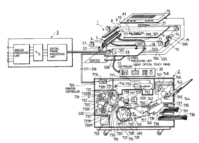
Fig. 1 shows an example of the internal
structure of a color image forming system embodying
the present invention. This system consists of an
upper digital color image reading unit 1 (hereinafter
called color reader), a lower digital color image
printing apparatus 2 (hereinafter called color printer),
and a video processing apparatus 3. Said color reader
1 is capable of color image information of an original
image in respective color components and converting
the same into electrical digital image signals by
means of color separating means to be explained later
and a photoelectric converting device such as CCD.
The color printer 2 is composed of an electrophoto-
graphic laser beam printer for reproducing colorimages of respective colors according to said digital
image signals and transferring said images plural
- 7 - 1 33 8 06 8
1 times in digital dot form onto a recording sheet.
The video processing apparatus 3 serves to convert
analog video signals, supplied from an external video
apparatus, into digital image signals for supply to
said color reader 1.
At first there will be explained the structure
of the color reader 1, in which there are shown an
original document 999; a platen glass 4 for supporting
the original document; and a rod-array lens 5 for
focusing the reflected light, from the original
illuminated by a halogen exposure lamp 10 onto a same-
size full-color sensor 6, and the above-mentioned
components 5, 6, 7, 10 constitute an original scanning
integral unit 11 for executing a scanning motion in a
direction Al. Color-separated image signals obtained
line by line in the course of the scanning motion are
amplified to a predetermined voltage level by a sensor
output signal amplifying circuit 7, and are supplied
by a signal line 501 to a video processing unit for
signal processing. Said line 501 is composed of a
coaxial cable for ensuring faithful signal transmission.
A signal line 502 serves for supplying driving pulses
6 for the same-size full-color sensor 6, and all
necessary pulses are generated in a video processing
unit 12. A white board 8 and a black board 9 for white
and black level correction of the image signals
respectively provide signal levels corresponding to
- 8 ~ 1338068
1 predetermined densities when illuminated by the halogen
exposure lamp 10.
A control unit 13, incorporating a micro-
computer, controls the display on an operation panel 20;
5 control of key input; control of the video processing
unit 12; detection of the position of the-original
scanning unit 11 by means of position sensors Sl, S2
through signal lines 509, 510; a stepping motor driving
circuit 15 for driving a stepping motor 14 for moving
the scanning unit 11 through a signal line 503;
on/off control and light intensity control of the
halogen exposure lamp 10 by means of an exposure lamp
driver 21 through a signal line 504; a digitizer 16
through a signal line 505; internal keys; an operation
unit and any other parts of the color reader 1, all
through a bus 508. The color image signals read by the
exposure scanning unit 11 in the course of scanning
motion are supplied, through the amplifying circuit 7
and the signal line 501, to the video processing unit 12.
In the following there will be explained the
color printer 2, wherein a scanner 711 is provided with
a laser unit for converting the image signals from the
color reader 1 into optical signals; a polygon mirror
712 for example of octagonal shape; a motor (not shown)
for rotating said mirror 712; and an f/0 lens (imaging
lens). There are also provided a mirror 714 for
deflecting the optical path of the laser beam, and a
~ 9 ~ 1338068
1 photosensitive drum 715. The laser beam from the
laser unit is reflected by the polygon mirror 712 and
linearly scans (raster scanning) the photosensitive
drum 715 through the lens 713 and the mirror 714, thereby
S forming a latent image corresponding to the original
-image.
There are further provided a primary charger
717, a whole-surface exposure lamp 718, a cleaner
station 723 for recovering the toner which has not been
transferred and thus remains on the drum; and a pre-
transfer charger 724, which are positioned around the
periphery of the photosensitive drum 715.
A developing unit 726 for developing the
electrostatic latent image formed on the photosensitive
drum 715 is provided with developing sleeves 731Y,
731M, 731C and 731Bk for effecting development in contact
with the photosensitive drum 715, toner hoppers 730Y,
730M, 730C and 730Bk for toner supply, and screws 732
for toner transfer, which in combination constitute
the developing unit 726 and are positioned around a
rotary shaft P thereof. For example, in case of forming
a yellow toner image, the development is conducted in
the illustrated position with the yellow toner, and,
in case of forming a magenta toner image, the developing
unit 726 is so rotated about the shaft P that the
developing sleeve 731M in the magenta developing unit is
brought to a position in contact with the photosensitive
-
- lo 1 338 0 68
1 drum 715. The development with cyan or black color is
also conducted in a similar manner.
There are further provided a transfer drum 716
for transferring a toner image formed on the photo-
S sensitive drum 715 onto the recording sheet; anactuator plate 719 for detecting the position of the -
transfer drum 716; a position sensor 720 for detecting
a home position of said transfer drum 716 when said
actuator plate 720 is brought close; a transfer drum
10 cleaner 725; a paper pressing roller 727; a charge
eliminator 728; and a transfer charger 729; which are
positioned around the transfer roller 716.
There are further provided paper cassettes
735, 736 containing recording paper (sheets); paper
15 feeding rollers 735, 736; and timing rollers 739, 740,
741 for regulating the timing of sheet feeding and
transportation. The sheet transported by these rollers
is guided by a paper guide 749, and, while the front
end thereof being held by a gripper to be explained
later, it is wound around the transfer drum 716 and
enters an image forming process.
There are further shown a drum motor 550 for
rotating the photosensitive drum 715 and the transfer
drum 716 in synchronization; a separating claw 750 for
separating the sheet from the transfer drum 716 after
the completion of the image forming process; a
conveyor belt 742 for transporting thus separated sheet;
338068
1 and an image fixing station 743 having a pair of heat-
pressure rollers 744, 745 for fixing the image of the
sheet transported by the conveyor belt 742.
Now reference is made toFigs. 2A and 2B for
explaining the details of the original scanning unit 11
and the video processing unit 12.
The color image signals supplied to the video
processing unit 12 are separated, in a sample hold
circuit S/H 43, into signals of green (G), blue (B)
0 and red (R). The separated color image signals are
subjected, in an analog color signal processing
circuit 44, to an analog process and an A/D conversion
to obtain digital color image signals. In the present
embodiment, the color image sensor 6 in the original
scanning unit 11 is composed of a staggered arrangement
of five areas, as shown in Fig. 2, so that a FIFO memory
46 is employed for compensating the aberration in the
reading position between the preceding channels 2, 4
and other channels 1, 3, 5. The compensated signals
from said FIFO memory 46 are supplied to a black
correction/white correction circuit for compensation for
unevenness in the dark characteristics of the color
image sensor 6, unevenness in the intensity of the
halogen exposure lamp 10 and unevenness in the sensi-
tivity of said sensor 6, utilizing the signals corre-
sponding to the reflected light from the aforementioned
white board 8 and black board 9. The color image data
- 12 - 1 3 3 8 0 68
1 proportional to the input light intensity to the color
image sensor 6 are subjected to a conversion, in a
logarithmic conversion circuit 86, for matching with the
relative sensitivity characteristics of human eyes,
5 and are supplied to a switching circuit 100 for
selecting either the color image signals from the video
interface 101 or those from the original scanning unit
11 .
It is to be noted that the apparatus of the
present embodiment constitutes an improvement on an
embodiment disclosed in Canadian Patent Application No
551,841, now Patent No. 1,281,363, of the present assignee.
Signals ITOP, BD, BCLK, VIDEO, HSYNC and
SRCOM (511 - 516) shown in Fig. 2 are interface
signals between the color printer 2 and the reader 1
shown in Fig. 1. Based on these signals, the image
signals VIDEO 514 read in the reader 1 are supplied to
the color printer 2. As shown in Fig. 14A, the synchro-
nization signal ITOP in the advancing direction of
image (sub-scanning direction) is generated four
times in an image frame, respectively corresponding
to the transfers of images of four colors (yellow,
magenta, cyan and black) in synchronization with the
rotation of the transfer drum 716 and the photosensitive
drum 715 in such a manner that the leading end of a
recording sheet wound on the transfer drum 716 in the
color printer 2 is in registration with the leading end
- 13 - 1338068
1 of the toner image at the transfer thereof in contact
with the photosensitive drum 715. Said signal is
supplied to the video processing unit in the reader 1,
and further, as an interruption signal (signal 511)
to a CPU 22 in the controller 13. Said CPU 22
executes image control in the sub scanning direction,
such as image editing, based on said interruption
signal. A synchronization signal BD 512 in the
direction of raster scanning (main scanning direction)
is generated once every rotation of the polygon
mirror 712, or every raster scanning. The image
signals read in the reader 1 are supplied to the
printer 2, by a main scanning line at a time, in
synchronization with said signal BD. A synchronization
clock siganl VCLK 513 serves to send 8-bit digital
video signals 514 to the color printer 2, by means of
flip-flops 32, 35 as shown in Fig. 14B. A main
scanning synchronization signal HSYNC 515 is generated
from the BD signal in synchronization with the VCLK
signal 513 and has a same repeating frequency as
that of the signal BD. Strictly speaking, the VIDEO
signals 514 are transmitted in synchronization with
said HSYNC signal 515. The BD signal 515, which is
generated in synchronization with the rotation of the
polygon mirror 712, contains the jitter of the motor
for rotating said polygon mirror 712, and will result
in jittering of the image if it is synchronized with
- 14 -
1 338068
1 said BD signal, so that the HSYNC signal 515 has to
be generated from the jitter-free VCLK signal, based
on the BD signal. SCROM is a signal line for semi-
duplex bidirectional serial communication. As shown
S in Fig. 14C, in synchronization with 8-bit serial clock
signals SCLK during a command busy signal CBUSY from
the reader, a command CM is released, in response to
which a status signal ST is returned from the printer
in synchronization with said clock signals. Said
status signal ST includes, for example a status
signal indicating that an image forming operation
is in progress, and an error status signal indicating a
sheet jamming or the like in the printer. This timing
chart shows a case in which a command "8EH" is responded
by a status signal "3CH". The information exchange,
including the commands from the reader to the printer,
such as the selection of color modes or cassettes, and
the status information from the printer such as sheet
jamming, absence of sheet or waiting state, is conducted
through said communication signal line SRCOM.
Fig. 14A is a timing chart showing the
transmission of an image of four colors, according to
the signals ITOP and HSYNC. The signal ITOP 511 is
generated every rotation or every two rotations of the
transfer drum 715, whereby the image data of yellow,
magenta, cyan and black are supplied respectively at
(1), (2), (3) and (4) from the reader 1 to the printer
1 338068
1 2 to form a full color image of said four colors on
the recording sheet. The HSYNC signal is released, for
example in case of an image of A3 size with a longi-
tudinal size of 420 mm with an image density of 16
s pel/mm in the image advancing direction, 420 x 16 = 6720
times. Said signal is simultaneously supplied to a
clock input port of a timer circuit 28 of the controller
13, whereby an interruption signal HINT 517 is supplied
to the CPU 22 after the count of a predetermined
number. In response the CPU 22 executes an image
control in the image advancing direction, such as
image extraction or image displacement.
In the following there will be explained the
fetching of the color image data in the video processing
unit 12 of the color reader 1, supplied from the video
processing apparatus 3.
Said fetching is set by a digitizer to be
explained in the following. Fig. 3 is an external
view of said digitizer 16, wherein shown are entry keys
427 for selecting inlay synthesis modes to be
explained later; a coordinate detecting plate 420 for
detecting the coordinate position for the purpose of
designating an arbitrary area on the original, or
an image magnification; and a pointer pen 421 for
designating coordinate positions.
On said coordinate detecting plate 420, there
are marked, in the upper right portion thereof, three
- 16 - 1 33 8 0 68
1 different sizes, namely image ratios of 100%, 200% and
300%, in the image recording on a recording sheet from
the video processing apparatus.
The image inlay synthesis from the video
5 processing apparatus 3 is conducted by depressing an
inlay synthesis key 427 shown in Fig. 3, and desig-
nating an inlay position with the pointer pen 421.
Said inlay area is for example a hatched area in Fig. 4,
and is identified, in response to the designation by
the digitizer 16, by a SYNC signal released from the
area signal generating circuit 51 in a section A - B
in the sub scanning direction, namely such as a SYNC
signal shown in Fig. 4. In Fig. 4, C indicates the
entire size of the original, and a hatched area is
the area designated by the digitizer. The SYNC signal
104 is sent to the video processing apparatus 3 through
the video interface 101 shown in Fig. 2.
In addition to said SYNC signal, the video
interface 101 provided with the video processing
apparatus 3 with the FREEZE signal 102 and the VCLK
signal 103, of which timing is shown in Fig. 5. The
FREEZE signal 102 and the SYNC signal 104 are generated
by the actuation of a start button in an operation unit
20. As shown in Fig. 5, the FREEZE signal 102 is shifted
to level "1" in response to said start button, while
the SYNC signal 104 is shifted to level "1" in a range
corresponding to the area designated by the digitizer
16.
- 17 ~ 1 33 8 0 68
1 However, in case the number of copies exceeds
one, and if the copy button is actuated after
resolving of an error such as sheet jamming in the
course of copying operation, the FREEZE signal 102
S is not shifted to the level "1", but the signals
SYNC 104 and VCLK 103 alone are supplied to the inter-
face 101. In the present embodiment a full-color
print is obtained by repating a color process 104
shown in Fig. 5, as indicated by the names of colors
shown therein.
In the following there will be explained
the function of the present embodiment, with reference
to a flow chart of the controller (CPU) shown in Fig. 11.
When the power supply is started, the
controller 13 reads the keys actuated on the operation
panel 20 and on the digitizer 16 (#01). If there is
actuated any key, there is discriminated whether said
key is a key instructing the start of copying operation
(#03), and the sequence proceeds either to #05 or
#23 respectively if said key has been actuated or not.
In the following there will be explained
the step #23 and the succeeding sequence when any key
other than the copy start key is actuated.
A step #23 discriminates whether an area for
inlay synthesis has been designated by a switch 427
shown in Fig. 3, and, if designated, the area designated
by the digitizer 16 is memorized (#25). On the other
- 18 - 1338068
1 hand, if not designated, there is discriminated
whether the number of prints has been designated (#27).
If the number of prints has been designated, said number
is stored in a register (#29). If it is not designated,
there is conducted a process for the other key (#31).
In the following there will be explained a
case in which the start of a copying operation is
designated in #03. When the start of copying operation
is instructed, there is at first discriminated whether
an error flag has been set (#05), and, if the error
flag has not been set, and, in the absence of the
error flag, there is generated the FREEZE signal 102
shown in Fig. 2 (#07), whereby image data are written
in a memory 303 in the video processing apparatus
to be explained later in relation to Fig. 7. Then
the error flag is reset (#09). Then an instruction
is given to the stepping motor driving circuit 15
shown in Fig. 1, whereby the scanner starts movement,
and the signal processing circuits shown in Fig. 1 are
activated in synchronization with the generated HSYNC
and VCLK signals. Thus the color component signals
are supplied to a color conversion circuit 50 shown
in Fig. 2 and then supplied to the color printer 2.
In response to the image signals supplied in succession
from the video processing unit 12, a drum 716 to be
explained later is rotated in response to the image
data supplied in succession from the video processing
1 338068
1 unit 12, and the image top signal ITOP is returned to
the unit 12 at each rotation. In the present embodi-
ment, a full-color print is obtained with four colors
of Y, M, C and Bk and requires, therefore, four
5 rotations of the drum 716.
Thus a step #13 discriminates whether the
ITOP signal has been supplied four times, and, if not,
there is discriminated whether an error has been
generated in the printer (#14). In the absence of
error, the sequence returns to #13. In the presence
of an error, an error flag is set, then the drive of
the scanner is stopped, and there is discriminated
whether the error state has been resolved (#21). On
the other hand, if the step #13 detects that the ITOP
signal has been supplied four times, indicating the
completion of a print, there is executed a decrement
of the print number register (#17). Then there is
discriminated whether the content thereof has reached
"0", and, if "0", the sequence returns to (A). On the
other hand, if not "0", the sequence returns to #11 to
continue the copying operation.
In the above-explained flow chart of the
embodiment, if an error occurs in the color printer
for example by sheet jamming (#14) in the course of a
printing operation of plural prints, the copying
operation is not restarted unless the copy start key is
actuated, since the sequence returns to (A) after the
- 20 - 1338068
1 error status is resolved.
Also since the error flag is set in the step
#19, the sequence proceeds from #5 to #11 when the copy
start key is actuated in the aforementioned state (A~,
a so that the FREEZE signal is not generated.in the #07.
Thus it is possible to prevent the storage of new
image signals in the memory 303.
In this manner the image data stored in the
memory 303 prior to said error are still retained,
and the errorneous storage of other data in said memory
can therefore be avoided.
The image data synchronization signal VCLK 103
in the video processing unit 12 is supplied to the
video processing apparatus 3, which supplies the video
interface 101 with color image signals 105, 106, 107
synchronized with said VCLK signal 103 and an enable
signal EN 108 indicating the effective range of said
image signals. When said EN signal 108 is "0" or "1",
the switching circuit 100 respectively selects the color
image signals from the logarithmic conversion circuit
86, or those from the video interface 101 for supply
to the succeeding circuit.
Though it is also possible to utilize the
aforementioned SYNC signal 104 as the control signal
for said switching circuit 100, the present embodiment
employs the EN signal from the video processing
apparatus 3 for this purpose, thereby achieving
-
- 21 -
1 338068
l following advantages.
If the above-mentioned SYNC signal is employed
for controlling the switching circuit 100, and if the
response of the video processing apparatus 3 is slow,
5 the switching circuit 100 is shifted over before the
output of the color image-signals-105, 106, 107,
whereby a black streak is formed at the switching
operation of the switching circuit 100, namely at an
ends of the inlay synthesis area of the image. On the
other hand, the present embodiment is capable of
preventing the formation of such black streak since
the switching circuit 100 is controlled by the EN signal
from the video interface 101.
The response of the video processing apparatus
3 becomes particularly slow, if image processing
involving plural pixels, such as edge enhancement, is
conducted therein.
Fig. 10 is a detailed circuit diagram of the
switching circuit 100, wherein data selectors 113 -
118 are composed of IC's such as 74LS157. Each dataselector selects one of two input data, according
to the signal 112 supplied to a selecting terminal S.
When the signal 112 is at the level "0", the selector
output lines Y570, M571 and C572 respectively select
the signals Y0 120, Mo 121 and C0 122, but, when said
signal 112 is at the level "1", there are respectively
selected the signals Y' 105, M' 106 and C' 107. Said
- 22 -
1 338068
1 selecting signal 112 is controlled, in addition to
the EN signal 108, by signals 110, 111 from the
controller 13. Also there are shown gates 125 - 128,
and a signal EN' corresponding to the logic sum of the
s EN signal 108 and the signal 121.
The switching circuit 100 selects the video
image signal, the image signal of a reflective
original (copying) or the inlay synthesis, according to
the states of the signals 110, 111, as will be
summarized in the following table:
Signal 110 Signal 111 Function
0 0 Reflective original
0 1 Video image
1 0 Inlay synthesis
1 1 Not possible
Thus, when the signal 110, 111 are at the level
"0", the image of the reflective original is trimmed
in an area designated by the digitizer 16. In the
following there will be explained the trimming of the
reflective original, with reference to Fig. 10. Such
trimming of the reflective original is conducted when
the signals 110, 111 shown in Fig. 10 are both "0".
In such case the exclusive-or signal 112 becomes "0",
whereby the signals Y120, M121 and C122 from the
logarithmic conversion circuit 86 are selected by the
selectors 113, 114, 115, 116, 117 and 118 and are
1 338068
1 released as the signals 122, 123 and 124. Also when
said signals 110, 111 are both "0", a signal 119 also
becomes "0", whereby the SYNC signal 120 from the
area signal generating circuit 51 is supplied directly
to AND gates 125, 126, 127.
In this manner the image signals 122,-123,
124 supplied to the AND gates 125, 126, 127 are
controlled by the SYNC signal 120. As the area signal
generating circuit 51 generates the SYNC signal
corresponding to the area designated by the digitizer
16, the trimming is conducted on the reflective
original, corresponding to the area designated by the
digitizer 16, in such case.
Also in response to the EN signal there are
controlled color correction, masking, gamma conversion
etc. according to the nature of the image. Said EN
signal 108 is supplied also to a color correction/
masking circuit 48 and a gamma conversion circuit 52
to be explained later.
Now reference is again made to Fig. 2. The
signals from the switching circuit 100 are supplied
to a black extraction (undercolor removal UCR) circuit
47 to generate a black component signal, which is
subtracted from the color signals 570, 571, 572. The
color correction/masking circuit 48 executes color
correction of the color image signals, in consider-
ation of the color separating filters in the color
image sensor 6 (Fig. 1) and the video processing
-
- 24 - 1338068
I apparatus 3.
In the following there will be explained the
function of the color correction/masking circuit 48.
There is already well known a masking correction,
s for the color component data Yi, Mi, Ci, according to
the following first-order calculation:
yO ayl -bMl -ccl
o ~aY2 bM2 cc2 Mi
CO -ay3 -bM3 Cc3 Ci
In the color correction/masking circuit 48
of the present embodiment, the coefficients are
rendered variable for the input image, by setting into
the CPU through the data bus 508.
More specifically, in the present embodiment,
lS the first matrix coefficients Ml or the second matrix
coefficients M2 can be set through a bus connected to
the controller 13:
ayl -bMl Cl
-aY2 bM2 -cc2
-ay3 -bM3 C3 /
~ Yl ~Ml rCl~
M2 Y2 ~M2 Yc2
\ ~Y3 ~M3 YC3/
The coefficients Ml serve for the correction
of the color separating filters in the original
scanning unit 11, and the coefficients M2 serves for
-
- 25 - 1338068
1 the correction of the video processing apparatus 3.
These two sets of the coefficients Ml, M2 are
selected by the EN signal 108 supplied from the video
interface 101. Thus the color correction is conducted
5 by selecting either the coefficients Ml in case of the
color image signals from the original scanning unit 11,
or the coefficients M2 in case of the signals from the
video processing apparatus 3. The output of the color
correction/masking circuit 48 is supplied to a color
conversion circuit 50, which in fact executes no
conversion in the present embodiment.
Numeral 52 indicates a gamma conversion circuit
for controlling the color balance and color density of
the output image, basically relying on data conversion
utilizing a look-up table, of which data are modified
by the inputs from the operation unit. The RAM 52 of
the present embodiment has at least two gamma character-
istics for each of yellow, magenta, cyan, black and mono-
color, as shown in Fig. 6, whereby the areas
A and B can be given different gamma characteristics in
a print.
The switching of the areas A and B is conducted
by the EN signal 108 from the video interface 101.
The gamma converting RAM 52 is so constructed
as to select characteristics for each color, and said
characteristic can be modified from the controller 13
by the actuation of liquid crystal touch panel keys on
- 26 - 1338068
1 the operation panel.
A variable magnification control circuit 53
and a 5-line buffer 54 modifies the image magnification
of the output signal of the gamma conversion circuit
52, and a-filter circuit 55 executes edge enhancement
and smoothing. The output of the filter circuit 55 is
supplied, through a printer interface circuit 56, to
the color printer 2.
Thus, in the present system, the color image
data from the video processing apapratus 3 are fitted
in the area designated by the digitizer 16, and optimum
color correction and gamma correction are made for the
original scanning unit 11 and for the video processing
apparatus 3.
In the following there will be explained the
structure of the video processing apparatus, with
reference to Fig. 7.
In Fig. 7 there are shown an NTSC decoder 300
for converting the input composite signal such as NTSC
signal into the signals R, G, B; a switching circuit
301 for selecting either the RGB input signals a or
the R, G, B signals from the NTSC decoder 300; an A/D
converter 302 for individual A/D conversion of the
R, G, B signals selected by the switching
circuit 301; a memory 303 for storing the signals
subjected to A/D conversion in the A/D converter 302
and having a capacity of at least a frame for each
1 338068
1 of the R, G, B signals; a digital filter 304 for edge
enhancement of smoothing on the signal read from the
memory 303; an enlarging interpolation circuit 305 for
effecting image enlargement with the signals filtered
s by the filter 304; and a complementary color
conversion table 306 for converting the R, G, B signals
interpolated by the interpolation circuit 305 into the
respectively complementary color signals Y, M and C.
A memory control circuit 308 controls the
reading, writing, refreshing and addressing of the
memory 303, and effects the writing of the memory 303
in response to the FREEZE signal entered through the
interface 307.
Said control circuit 308 also receives a
vertical synchronization signal VDTV 363 of television,
a field discrimination signal FLDTV generated from a
SYNC circuit 321, the output signal of the switching
circuit 309, the output signal of a SYNC detecting
circuit 310, and the output signal of a magnification
selecting switch 322. Said control circuit 308 also
generates an area signal 366 triggered by said SYNC
signal and indicating the effective area of the memory
303. The switching circuit 309 receives a television
clock signal C/TTV 36a, a horizontal synchronization
signal HDTV 362, an interface clock signal VCLK 103,
and the aforementioned SYNC signal 104, and selects
either the signals VCLK 103 and SYNC 104, or the
- 28 - 1 33 8 06 8
1 signals CKTV and HDTV respectively when the SYNC
detecting circuit 310 detects the presence or absence
of the SYNC signal.
There are further provided a gate 311 for logic
calculation of the area signal 366 and the SYNC signal
104; a delay circuit 312 for compensating the delay
caused by the data latching in the filter 304 and the
enlarging interpolation circuit 305; delay circuits
313 - 315 for compensating the delay caused by
filtering in the filter 304, wherein the delay circuit
313 has a delay time of 5 horizontal lines, while the
circuit 314 has a delay time of 7 horizontal lines,
and 315 is an AND gate; and delay circuits 316 - 318 for
compensating the delay caused by the enlarging inter-
polation executed in the enlarging interpolationcircuit 305, wherein the delay circuit 316 has a delay
time of 1 horizontal line, while the delay circuit 317
has a delay time of a pixel, and the delay circuit 318
serves for compensating the delay caused by the data
latching in the aforementioned complementary color
conversion table 306.
The above-mentioned delay circuits 312, 313,
314, 316 and 317 are driven by the aforementioned
signals DVCK 367 and DVSH 368. When the enlarging
ratio is modified by the selecting switch 322, the
repeating period of said signals is also varied, so
that the delay time of the aforementioned delay
-
- 29 -
1 338068
1 circuits is also changed.
Numeral 320 is an AND gate for generating the
logic product of the SYNC signal 104 and the output
signal ENl of the delay circuit 318.
S In the following there will be explained the
function of the embodiment explained above. In the
video processing apparatus 3, either the R, G, B
signals a entered in response to the FREEZE signal
102 supplied from the video processing unit 2, or the
R, G, B signals 355 - 357 obtained by decoding of the
NTSC signal b with the NTSC decoder 300, are selected
by the switching circuit 301, then digitized by the
A/D converter 302 according to the CKTV signal
361 obtained from the SYNC circuit 321, and stored
in the memory 303. In the present embodiment, the
number of pixels of said memory is selected as 640 x
480. The timing of the reading, writing and refreshing
of the memory 303 is controlled by the memory control
circuit 308. When the SYNC signal 104 is not entered
from the video processing unit 12, the SYNC detecting
circuit 310 identifies the absence of the SYNC signal,
whereupon the switching circuit 309 selects the
synchronization signals CKTV 361 and HDTV 362 of the
television. On the other hand, when the SYNC signal
104 is entered from the video processing unit 12, the
switching circuit 309 selects the signals VCLK 103 and SYNC
104, whereby the memory 303 is read with the timing of
1 338068
1 the signals VCLK 103 and SYNC 104 entered through the
interface.
The image magnification of the video image to
be inlaid in the image of the reflective original 999
is fixed to 100%, 200% or 400%, which are selected by
the magnification selecting switch 322. The output
signal thereof is supplied to the memory control circuit
308 thereby controlling the data reading from the
memory 303. In case of the image magnification of
200%, the pixels of a line are read twice, and, in
case of 400%, they are read four times. In each
magnification of 100%, 200% or 400%, the synchroniza-
tion of the memory 303, filter circuit 304 and enlarging
interpolation circuit 305 is achieved by the memory
control circuit 308, in synchronization with the
signals DVCK 365 and DVHS 366.
The signals read from the memory 303 are
subjected to edge enhancement or smoothing by a
filtering with matrix calculation of 5 x 7 pixels in
the filter circuit 304, then to interpolation for the
image magnification of 200% or 400% in the enlarging
interpolation circuit 305, further to the conversion
of the R, G, B signals respectively into the signals
C107, M106 and Y105 by the complementary color
conversion table 306, and transferred to the video
processing unit 12 through the reader interface
circuit 307.
- 31 - 1 33 8 0 68
1 In the present embodiment, the R, G, B data
read from the memory 303 are processing in so-called
pipeline structure involving the filter circuit 304,
the enlarging interpolation circuit 305 and the
complementary color conversion table 304, so that a
delay in time is inevitable from the data input to
the data output in each circuit. Therefore, since
the video processing apparatus 3 executes processes
of plural stages, there is required a predetermined
time from the instruction of image output to the
actual output. In order to compensate said delay,
the present embodiment employs the EN signal 108
generated from the interface. The delay circuits
312, 314, 317, 318, the delay circuits in the scanning
line direction 313, 315, and the gates 315, 318 cause
delays same as the delay times in the circuits 303,
304, 305 and 306, and the EN signal 108 is rendered
effective during the release of the effective image
data C107, M106 and Y105.
In the present embodiment, there are employed
640 x 480 pixels for achieving a 1 : 1 mesh ratio
(ratio of vertical size to horizontal size of a pixel),
and such image data are released for realizing an
image magnification of 100%, 200% or 400%. However,
in this state, the SYNC signal 104 supplied to the
interface 307 may not match the size of the enlarged
image data. For this reason the memory control circuit
- 32 - 1 338 068
1 308, for controlling the memory 303, generates an image
area signal 366 indicating the image size to be read
by the SYNC signal 104, namely 640 x 480 pixels (or
1280 x 960 pixels in case of the magnification of 200%
or 2560 x 1920 pixels in case of magnification of 400%).
Then the gate 311 produces the logic product of said
area signal 366 and the SYNC signal 104, and the gate
320 produces the logic product of the output ENl 371
from the delay circuit 319 and the SYNC signal 104.
In this manner, if the area for inlay synthesis indicated
by the SYNC signal is larger than the image output
area, the area of the EN signal 108 is limited by
the image area signal 366. On the other hand, if the
area of the SYNC signal 104 is smaller, the image
area is forcedly limited to the area of said SYNC
signal. These operations are shown in Figs. 8A and 8B,
which show the SYNC signal 104, area signal 366, END
signal 370, EN signal 108 and image data 105 - 107,
respectively in a case in which the SYNC signal is
longer in duration than the area signal, namely a
case in which the size of the image to be fitted is
smaller than the area for fitting, and a contrary case
in which the size of the image is larger than the
area for fitting.
In Figs. 8A and 8B, a duration D indicates the
delay time caused by the delay circuits 212 - 318
shown in Fig. 7.
~ 33 ~ 1 338068
1 As explained in the foregoing, the filter
circuit 304 constitutes a filter through calculation
of the values of pixels in a 5 x 7 window. This
reduces the effective image area by a line to several
lines, but such reduction is practically negligible.
The delay circuits 316, 317 and the gate 318 for the
enlarging interpolation circuit 305 have a similar
function.
In the following there will be explained the
printed image obtained after image synthesis, with
reference to Fig. 9. The area for video image inlay
is designated by two points a, b with the digitizer 16.
According to thus designated area, the SYNC signal 104
is supplied from the video processing unit 12 to the
video processing apparatus 3, which in response sends
the video image signals C107, M106, Y105 to the video
processing unit 12 in said area. If the area designated
by the digitizer 16 is larger as shown in Fig. 9A, the
video processing apparatus 3 releases the EN signal 108
indicating the effective area of the video image, and
the video processing unit 12 fits the video image
only in the area indicated by said EN signal 108.
Outside said area, the image of the original 999 placed
on the color image reader 1 is printed. On the other
hand, if the area a-b designated by the digitzer 16 is
smaller than the effective area of the video image as
shown in Fig. 9B, the area of inlay synthesis is
-
~ 34 ~ 1 33 8 068
1 defined by the SYNC signal 104. As the result the
inlay synthesis of the video image is made in the
hatched area.
The memory 303 of the present embodiment is
composed for example of a DRAM, so that a refreshing
operation is required for remaining the stored data.
In the ordinary storage of the memory content, or at
the writing of the video signals (RGB signals or NTSC
signals) entered by the FREEZE signal 102, or the
retaining of the stored data, refreshing singals are
generated according to the timing of the HDTV signal
362. Also, at the memory reading by the SYNC signal
104 supplied from the video processing unit 12, said
refreshing signals are generated according to the
timing of the SYNC signal 104. Since the repeating
period of the HDTV signal 362 is significantly
different from that of the SYNC signal 104 (they are
different by about four times in the present embodi-
ment), the number of refreshing operations is modified
for each signal.
In the following there will be detailedly
explained the structure of the memory control circuit
308, with reference to Fig. 12.
In Fig. 12, signals SCK (selected clock) and
25 SHS (selected horizontal signal) are selected by said
switching circuit 309 for supply to the memory control
circuit 308. There are also shown a frequency divider
1 338068
1 370 for dividing the frequency of the signal SCK with
a variable dividing ratio according to the setting of
the magnification setting switch 322; a frequency
divider 372 for dividing the frequency of the signal
5 SHS with a similarly variable dividing ratio; a
quaternary counter 374 for counting the output of the
frequency divider 370; a counter 376 for counting the
address in the main scanning direction; a counter 378
for counting the address in the sub sCAnn;ng direction;
a comparator 380 for comparing the count of the
counter 376 with the output of an area value 382; and
a comparator 384 for comparing the count of the counter
378 with an area value 386. The values 382, 386 are set
in advance at the numbers of pixels in the horizontal
and vertical directions of the image memory 303.
Thus, when either of the outputs of the
comparators 380, 384 is shifted to the L-level, the
output of the gate 388 and the area signal are like-
wise shifted to the L-level.
A logic circuit 390 produces, from the 2-bit
output of the quaternary counter 374, a RAS (raw address
strobe) signal (B), a CAS (column address strobe)
signal (C) and a signal (D) for controlling a selector
391 to be explained later, as shown in Fig. 13A. There
are further provided a selector 391 for selecting either
the output of the counter 376 or that of the counter
378 as the memory address, in response to the
- 36 - 1 338 0 6 8
above-mentioned signal (D); a selector 392 for
supplying the memory 303 with either the above-
mentioned signals (B), (C) or refreshing signals (C),
(D) shown in Fig. 13B; a D-flip-flop 393 for fetching
5 the SHS signal from the switch circuit 309 through an
inverter 397, and giving the output to the enable
terminal of the quaternary counter 395; a quaternary
counter 395 for counting the SCK signal from the
switch circuit 309; a logic circuit 394 for generating,
10 from the 2-bit output of the counter 395, signals *RASY
(C) and *CASY (D) shown in Fig. 13B; and a counter 396
to be enabled according to the output of the quaternary
counter 395. Said counter 396 is set at "32" or "8"
respectively when the SYNC detecting circuit 310
15 identifies the presence or absence of the SYNC signal,
and counts the SCK signal downwards, providing the
output to the clear terminal of the D-flip-flop 393.
AND gates 398, 400 and an inverter 399 enable a
JK-flip-flop 368 according to a read/write signal R/W
20 from the controller 13 and a FLD signal from the SYNC
circuit 321 shown in Fig. 7. An OR gate 401 selects
the output Q of the JK-flip-flop 368 or the signal R/W
for supply to the enable terminal of the counter 378.
In the following there will be explained the
25 function of the above-explained memory control circuit
308.
At first there will be explained a case of
~ 37 ~ 1 3 3 8 0 6 8
1 writing instruction from the controller 13. In this
case the R/W from the controller 13 is at the H-level,
whereby the counter 378 is enabled, and the output Q
of the JK-flip-flop 368 is determined according to the
a level of the FLD signal. The JK-flip-flop 368 indicates
the vertical address of the memory 303 in cooperation
with the counter 378. The output of the JK-flip-flop
368 indicates the lowermost bit of the vertical address,
while the output of the counter 378 indicates other bits.
Consequently, when the FLD signal is at the L-level
indicating an odd field, the output Q of the JK-flip-flop
is fixed at the H-level, whereby odd addresses alone
are released as the vertical addresses. On the other
hand, when the FLD signal is at the H-level indicating
an even field, the output Q of the JK-flip-flop 368
is fixed at the L-level whereby even addresses alone
are released as the vertical address.
On the other hand, the horizontal addresses are
generated by the frequency divider 370, quaternary
counter 374 and counter 376.
The horizontal and vertical addresses
generated in this manner are selected, as the memory
address, by the selector 391 according to the output
of the logic circuit 390. The signals RAS, CAS are
generated in synchronization with said horizontal and
vertical addresses as shown in Fig. 13A, thereby
effecting the writing operation. In this case the
-
- 38 - 1338068
selector 392 provides the memory 303 with the signals
from the logic circuit 390.
In the following there will be explained a
case in which a reading signal is supplied from the
controller 13.
In such stage the R/W signal is shifted to the
L-level, whereby the output of the JK-flip-flop 368
becomes independent from the FLD signal, and said
flip-flop 368 and the counter 378 constitute a single
counter. Consequently, different from the writing
operation, the vertical address is increased by one
at a time.
Also in the reading operation, when a blanking
period is started by the downshift of the SHS signal,
the output signal access/refresh of a D-flip-flop 393
is inverted to the H-level to realize the refreshing
state for the memory 303. In this state, the selector
392 provides the memory 303 with signals RAS r, CAS y
generated by the logic circuit 394 for refreshing (shown
in Fig. 13B), whereby the memory 303 automatically
executes the refreshing operation.
Also in this case, the counter 396 is set at
a value corresponding to the signal from the SYNC
detecting circuit 310, for example "32" or "8" re-
spectively when said detecting circuit 310 identifies
the presence or absence of the SYNC signal. This is
because of the aforementioned necessity of varying the
- 39 ~ 1338068
1 timing of refreshing operation, based on the difference
in repeating period of the HDTV signal 362 and the SYNC
signal 104.
Also in the reading operation, the dividing
ratios of the frequency dividers 370, 372 are modified
according to the image magnification, thus extending
the repeating period of the pulses supplied to the
counter 376, 378 in case of an image enlargement.
Also the gate 388 releases the area signal 366,
according to the comparison of the area values 382, 386
with the counts of the counters 376, 378.
In the following there will be explained the
structure of the color printer 2, for printing the
image signals processed in the video processing unit
12, while making reference to Fig. 1. In Fig. 1, a
scanner 711 is provided with a laser unit for con-
verting the image signals from the reader 1 into
optical signals; a polygon mirror 712 for example of
octagonal shape; a motor (not shown) for rotating said
mirror 712; and an f/~ lens (imaging lens) 713. There
are further provided a mirror 714 for deflecting the
optical path of the laser beam; and a photosensitive
drum 715. The laser beam from the laser unit is
reflected by the polygon mirror 712, and linearly
scans (raster scanning) the photosensitive drum 715
through the lens 713 and the mirror 714, thereby
forming a latent image corresponding to the original
image.
- 40 ~ 1 3 38 0 68
1 There are further provided a primary charger
717, a whole-surface exposure lamp 718, a cleaner
station 723 for recovering the toner which has not been
transferred and thus remain on the drum; and a pre-
S transfer charger 724; which are positioned around the
periphery of the photosensitive drum 715. A developing
unit 726 for developing the electrolatent image formed
on the photosensitive drum 715 by the exposure to
laser beam is provided with developing sleeves 731Y
(yellow), 731M (magenta), 731C(cyan) and 731Bk (black)
for effecting development in contact with the photo-
sensitive drum 715, toner hoppers 730Y, 730M, 730C and
730Bk for toner supply, and screws 732 for toner transfer,
which in combination constitute the developing unit 726
and are positioned around a rotary shaft P thereof.
For example, in case of forming a yellow toner image,
the development is conducted in the illustrated
position with the yellow toner, and, in case of forming
a magenta toner image, the developing unit 726 is so
rotated about the shaft P that the developing sleeve
731M in the magenta developing unit is brought to a
position in contact with the photosensitive drum 715.
The development with cyan or black color is also
conducted in a similar manner.
There are further provided a transfer drum 176
for transferring a toner image formed on the photo-
sensitive drum 715 onto the recording sheet; an actuator
-
- 41 - 1 33 8 0 6 8
1 plate 719 for detecting the position of the transfer
drum 716; a position sensor 720 for detecting a home
position of said transfer drum 716 when said actuator
plate 720 is brought close; a transfer drum cleaner
725; a paper pressing roller 727; a charge eliminator
728; and a transfer charger 727; a charge eliminator 728;
and a transfer charger 729; which are positioned around
the transfer roller 716.
There are further provided paper cassettes
735, 736 containing recording paper (sheets); paper
feeding rollers 735, 736 for feeding sheets from the
cassettes 735, 736; and timing rollers 739, 740, 741
for regulating the timing of sheet feeding and trans-
portation. The sheet transported by these rollers
is guided by a paper guide 749, and, while the front
end thereof being held by a gripper to be explained
later, it is wound around the transfer drum 716 and
enters an image forming process.
There are further shown a drum motor 550 for
rotating the photosensitive drum 715 and the transfer
drum 716 in synchronization; a separating claw 750
for separating the sheet from the transfer drum 716
after the completion of the image forming process; a
conveyor belt 742 for transporting shut separated
sheet; and an image fixing station 743 having a pair of
heat-pressure rollers 744, 745 for fixing the image of
the sheet transported by the conveyor belt 742.
- 42 - 1 3 3 8 0 68
1 In the above-explained structure, a latent
image corresponding to yellow is at first formed on
the photosensitive drum 715 by the exposure to the
laser beam, then developed with the developing unit
s 731Y and transferred onto the sheet on the transfer
drum 716. Subsequently the developing unit 726 is
rotated about the illustrated shaft P. Then a latent
image corresponding to magenta color is formed on the
photosensitive drum by the exposure to laser beam,
and is subsequently process in a similar manner.
This operation is repeated also for cyan and black
colors. Upon completion of the image formation, the
sheet is separated by the separating claw 750, and is
subjected to image fixation in the fixing station 743,
whereby a print of the color image is completed.
In the foregoing embodiment, the means for
designating the area of image inlay is composed of the
digitizer shown in Fig. 3, and the video processing
apparatus 3 is employed as means for supplying image of
a predetermined size, to be fitted into said area.
Also there is provided means for providing a
portion between the area designated by said designating
means and the area of the image supplied by said
supplying means, with another image different from
said image, in such a manner that the image from the
video processing apparatus is fitted only in the smaller
one of the area designated by the digitizer and the
- 43 _ 1 33 8 0 68
1 area of the image from the video processing apparatus 3,
and the switching circuit 100 is controlled in such a
manner that, if the area designated by the digitizer is
larger than the area of the video image, the image from
5 the original scanning unit 11 is fitted in the portion
between said areas.
Thus the foregoing embodiment is capable of
satisfactory image synthesis without blank, in-the
synthesis of plural images.
In the foregoing embodiment, the means for
designating the area of image inlay is composed of the
digitizer shown in Fig. 3, and the video processing
apparatus 3 is employed as means for supplying image
of a predetermined size, to be fitted into said area.
Also there is provided means for preferentially
effecting inlay synthesis in the smaller one of the area
designated by said designating means and the area of
the image supplied by said supplying means, in such a
manner that the image from the video processing
apparatus is fitted only in the smaller one of the area
designated by the digitizer and the area of the image
from the video processing apparatus 3, and the
switching circuit 100 is controlled in the above-
mentioned manner.
Thus the foregoing embodiment is capable of
satisfactory image synthesis without blank, in the
synthesis of plural images.
-
- 44 - 1 3 3 8 0 6 8
1 Also in the foregoing embodiment, the
switching circuit 100 controlled by the area signal
generating circuit 51 is employed as means for synthe-
sizing the externally supplied video signals in a
S predetermined position of the original image, and is
used as a gate for controlling the trimming means
which controls the trimming of image in copying of an
original image, according to the signals 110, 111
from the control unit. Besides the designating means
of the present invention is composed of the digitizer
shown in Fig. 3.
However the present invention is not limited to
such embodiment, and there may naturally be employed
other designating means, such as a mouse.
As explained in the foregoing, the present
invention enables designation of the synthesizing
position of video signal and of the image area in
original copying with a simple structure, thereby
simplifying the operation.
Furthermore, in the foregoing embodiment, the
means for synthesizing a first input image signal and
a second input image signal is composed of the
switching circuit 100, for synthesizing the image from
the video processing unit 3 and the image from the
original scanning unit, but the present invention is
not limited to such embodiment. The present invention
is effectively utilized upon synthesizing two images.
-- 1 338068
- 45 -
1 Furthermore, means for generating a switching
signal for the first and second input image signals is
composed of the area signal generating circuit Sl which
is controlled by the digitizer 16, but there may be
S employed other instructing means such as a mouse.
Furthermore, control means for switching the
state of synthesis of the synthesizing means with a
predetermined delay from the instruction signal is
composed of circuits 312 - 320 in the video processing
apparatus 3. More specifically, in said embodiment,
an instruction signal 105 is given to the video
processing unit 3, which in response executes a
processing and releases the image data after a pre-
determined delay, and the unit 3 simultaneously supplies
lS the switching circuit 100 with the switching EN signal
108. However the present invention is not limited by
such embodiment, and a signal corresponding to said
EN signal 108 may be directly generated by the circuit
51 without the intervention of the video processing
unit.
As explained above, the foregoing embodiment
is capable, for example in synthesizing two images,
of satisfactory synthesis at the peripheral portion of
the area of image synthesis.
Furthermore, in the foregoing embodiment, an
error in the course of a printing operation is
detected by a step #14 shown in Fig. 11, and, in case
- 46 - 1 338 068
1 of detection of an error, steps #07 to #09 are executed
to prohibit new storage in the memory 303, at a new
print start instruction.
Therefore the foregoing embodiment can realize
5 operability without uneasy feeling to the operator.
Furthermore, in the foregoing embodiment, the
memory requiring periodical refreshing is composed of
the memory 303; a first synchronizing system for
generating the synchronization signal for said
refreshing operation is composed of the SYNC circuit
321; a second synchronization system, not synchronized
with said first synchronizing system, is composed of
the system control pulse generator 57 shown in Fig. 2;
and control means for switching the first and second
synchronization systems with the switching circuit 309
shown in Fig. 7 is composed of the counters 396, 395
and the D-flip-flop 393.
However, it is also possible, instead of
switching the synchronization signals from such
synchronization systems, to vary the repeating period
of the synchronization signal itself.
As explained in the foregoing, the present
invention enables secure refreshing operation even at
the switching of the synchronization system for the
purpose of refreshing operation, thereby preventing the
destruction of the information stored in the memory.