Note: Descriptions are shown in the official language in which they were submitted.
` 1 3381 55
. BIDIRECTIONAL BUFFER WITH LATCH
AND PARITY CAPABILITY
Technical Field of the Invention
The present invention relates generally to digital
signal processing circuits and more specifically to a
bidirectional receiver/driver buffer circuit
incorporating a latch and~circuit apparatus for both
generating and verifying parity as a function of the
data at the latch.
Summary of the Invention
A principal object of the present invention is to
provide apparatus for buffering and parity checking
digital data communicated between two data buses which
permits parity to be generated responsive to the data
without interrupting either of the data buses.
Another object of the present invention is to
provide such an apparatus including new and improved
latch and driver circuits which provide increased speed
of operation.
A further object of the present invention is to
-
- - 1 3381 55
provide a truly transparent latch circuit which
provides latching of data without imposing any
significan~t delay between input and output devices.
Yet another object of the present invention is to
provide a driver including a phase splitter circuit
which provides the driver with increased speed but --
requires no significant increase in power consumptiOn.
In accordance with the present invention,
apparatus is provided for buffering and parity chec~ing
digital data communicated between first and second data
buses. This apparatus comprises a plurality of
bidirectional bit buffer circuits, each of the
bidirectional bit buffer circuits including: a first
data path comprising a receiver having an input
connected to said first data bus, a latch having an
input connected to the output of said receiver, and a
driver having an input connected to the ou~put of said
latch and an output connected to said second data bus;
a second data path comprising a receiver having an
input connected to said second data bus, a latc~ having
an input connected to the output of said receiver, and
a driver having an inpu~ connected to the output of
said latch and an output connected to said first data
bus; means for controlling the drivers to selectively
place the output of the drivers in an active driving or
high impedance state; and means for controlling the
data latches to selectively latch or pass through data.
Further provided are parity generating means connected
at the output of the latch in the first data path of
each of the bidirectional bit ~uffer circuits for
generating a parity signal responsive to the data at
the output of said first data path latches.
In a preferred embodiment of the invention, the
above described apparatus is implemented using new and
improved transparent latch and driver circuits.
A transparent latch circuit is provided which is
responsive to a logical control signal for holding a
data signal at a circuit node. This transparent latch
FI9-88-OlO ~ 2-
1 3-3 ~ 1 55
... ;... . .
circuit comprises: means connected to the circuit node
~ for applying the data signal to the circuit node; means
connected to the circuit node for sensing the data
signal; latch means connected to the circuit node in a
T-connection with the data applying and sensing means
for selectively holding the data signal; and actuating
means connected to the latch means for actuating the
latch means to pass through the data signal or hold the
data signal on the circuit node regardless of the state
of the data applying means.
- A driver circuit is provided of the type
responsive to a logical input signal applied to an
input terminal for actuating first or second driving
means, the first driving means actuable to provide a
logical high signal level at an output terminal, the
- second driving means actuable to provide a logical low
signal level at the output terminal. This driver
circuit includes a phase splitter circuit comprising: a
first transistor for providing current from a first
terminal to a second ter~inal in accordance with a
signal applied at a control terminal thereof, the first
transistor having a control term; n~ l connected to the
input terminal and a second terminal connected to a
reference potential; means for applying a supply
voltage to the first te~minal of the first transistor;
the first terminal of the first transistor connected to
the first driving means; a second transistor having a
second terminal connected to the input terminal; means
for applying said supply voltage to the control
terminal of the second transistor; and the first
terminal of the second transistor being connected to
the second driving means.
Brief DescriPtion of the Drawings
These and other objects, features, and advantages
of the invention will be apparent from a consideration
of the following description and drawings, in which:
FIG.l is a block diagram of a buffer and parity
FI9-88-OlO -3-
- 1 338 1 55
generating ~ircuit constructed in acc~rdance with the
prior art and described hereinabove;
FIG.2 is a block diagram of a buffer and parity
generating circuit constructed in accordance with the
present invention;
FIG.3A is a schematic diagram of the receiver and
latch circuits of FIG. 2 implemented in bipolar
transistor logic;
FIG.3B is a schematic diagram of the driver
circuit of FIG.2 implemented in bipolar transistor
logic;
FIG.4 is a block diagram of a transparent latch
circuit constructed in accordance with the prior art;
and
FIG.5 is a simplified block diagram illustrating
the logical connections of the transparent latch
circuit constructed in accordance witi the present
invention.
Background of the Invention
Referring first to FIG.1, a circuit 10 is shown
for bidirectionally buf~ering digital signals between,
for example, first and second digital signal buses 12,
14. For purposes of explanation, buses 12, 14 will be
described as 8 bit data buses.
Circuit 10 includes eight, generally parallel
connected, bidirectional bit buffer circuits, indicated
at B0-B7. Bit buffer circuits B0-B7 are identical in
construction, and only circuit B0 is described and
shown in detail herein.
Bit buffer circuit B0 comprises two generally
parallel bit buffer paths, the first path comprising a
receiver 16, latch 18, and driver 20 connected
seriatim. In the second of the bit buffer paths, a
receiver 22, latch 24, and driver 26 are also connected
i
FI9-88-010 -4-
1 3381 55
seriatim, and in opposite order to the corresponding
components of the first path. Receivers 16, 22
comprise conventional logical bit receivers. Drivers
20, 26 comprise conventional logical bit drivers, each
including a control terminal 28, 30, respectively, for
selectively placing the output in an active or a `
high-impedance state. Latches 18, 24 comprise
conventional transparent latches, each including a
control terminal 32, 34, respectively, for selectively
placing the latch in a latched or pass-through (i.e.
transparent) state.
A parity generator 36 is provided, the inputs of
the parity generator being connected to the inputs of
receivers 16 in each of circuits B0-B7. Parity
generator 36 comprises a conventional parity "tree" of
logical exclusive-OR gates. For purposes of
explanation, a memory device 38, for example a dynamic
random access memory (RAM), is shown connected to data
bus 14.
In operation, circuit 10 functions generally to
bidirectionally buffer data between buses 12 and 14.
In one exemplary application, buses 12, 14 function as
local data buses in a computer system (not shown), with
bus 12 interfacing a microprocessor and bus 14
interfacing memory 38. In accordance with its
buffering function, when data i-s to be communicated
from bus 12 to bus 14, an appropriate signal is applied
to control terminal 30 so as to place driver 26 in a
high impedance state. Data, in the form of a high or
low logical bit 0, is sensed by receiver 16 and
converted to another logical level (i.e. 1 or 0).
Receiver 16 thus functions in a standard manner to
convert widely ranging levels of input signals to
narrower ranging levels of output signals. A signal is
applied to control terminal 32 for appropriately
latching or passing bit 0 through latch 18. The data
at the output of latch 18 is then sensed by driver 20,
which is controlled via terminal 28 so as to be in the
FI9-88-010 _5_
.
., . 1338155
-- active mode for driving bus 14. Data ,s transmitted in
substantially the identical manner from bus 14 to bus
12 via the path including receiver 22, latch 24, and
driver 26.
Parity generator 36 provides the capability to
generate a parity bit responsive to the data on bus 12.
When such parity generation is desired, the data on bus
12 is frozen for a time sufficient to permit parity
generator 36 to operate on the data and generate the
parity bit. Parity generator 36 further provides the
capability to generate a parity bit responsive to the
data on bus 14, with the data either being latched in ~-
or passed through latch 24.
When applied in a computer environment of the type
described above, circuit 10 exhibits the substantial
disadvantage of interrupting data transmission on bus
12 whenever it is desired to generate a parity bit.
Mcre specifically, when parity is generated responsive
to data on bus 12, the data must be frozen on bus 12
for a time sufficient to allow parity generator 36 to
function. Similarly, when it is desired to generate a
parity bit responsive to the data on bus 14, the data
must be frozen on bus 14 or latched in latch 24. In
either of these conditions, the data is present at the
output of driver 26, ana thus it is necessary to
interrupt data transmission on bus 12.
Detailed Description of the Invention
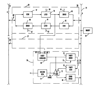
Referring now to FIG.2, a circuit 50 constructed
in accordance with the present invention comprises
eight bidirectional bit buffer circuits C0-C7 connected
intermediate a pair of data buses 52, 54, and a parity
generating and checking circuit 56. Circuits C0-C7 may
conveniently be identical in construction, each
bidirectionally buffering a single bit line (not shown)
between data buses 52, 54. For purposes of
explanation, only circuit C0 is shown and described in
detail.
Circuit C0 comprises two parallel connected data
paths, the first path comprising a receiver 57, a latch
58, and a driver 60 connected seriatim between buses
52, 54, respectively. The second data path in circuit
C0 comprises a receiver 62, latch 64, and driver 66
connected seriatim between buses 54, 52 respectively.
Drivers 60, 66 each include a control terminal 61, 67,
respectively, for selectively placing their outputs in
FI9-88-010 -6-
. ,.
.
1 3381 55
, . ` .
- either an active driving or high impedance state-
Latches 58, 64 each include a control terminal 59, 63,
respectively, for selectively latching or passing
through the data at their inputs. Preferred
S embodiments of these componentS are described herein
below. - -
Continuing to describe FIG.2, a parity generatingcircuit 68 is connected at the output of latch 58 of
circuit C0, and to the output of the corresponding
latches in circuits C1-C7. Parity generator 68 is thus
positioned to generate a parity bit responsive to the
data at the output of the latches. Parity generator 68
preferably comprises a logical exclusive-NOR tree of
the type shown in IBM Technical Disclosure Bulletin
Volume 16, No. 10, page 3249.
Parity generator 68 is connected at its output to
bot~ the input of a parity driver circuit 70 and the
input of a logical exclusive-NOR gate 72. Parity
driver circuit 70 includes a control terminal 73 for
selecting an active driving or high impedance output
state, this ~ontrol terminal being connected to the
output of a gen/chk (i.e. generate or check parity)
receiver 74 and to an enable terminal 76 on gate 72. A
parity receiver 78 has an input 79 connected in common
with the output of parity driver 70, and an output
connected to a second input of gate 72. An error
driver 80 is connected at its input to the output of
gate 72. For purposes of explanation, a memory device
84, for example a dynamic RAM memory, is shown
connected to bus 54. Gate 72, receivers 74, 78, and
drivers 70, 80 comprise conventional circuits.
In operation, through the application of
appropriate signals to latch control terminals 59, 63,
driver control terminals 61, 67, 73, and the inputs for
receivers 74, 78, circuit 50 can be operated to
generate parity for data on either of buses 52, 54
without interrupting the operation of the buses.
Circuit 50 can further be operated to check the parity
FI9-88-010 _7_
1 338 1 55
of data on either of the buses against a stored parity
bit. Upon consideration of the operation of circuit 50
as described below, many useful buffering and parity
related functions will become apparent to the reader.
For purposes of explanationj the operation of
circuit 50 will now be described with respect to block
diagram FIG.2. Described first will be the operation
of circuit 50 required to generate a parity bit
responsive to the data on bus 52 and drive that parity
bit with the associated data onto bus 54. To perform
this function, control terminal 59 is operated to hold
the data on bus 52 in latch 58, bus 52 then being free
for subsequent data communication. Driver 60 is
controlled via terminal 6l to place it in its high
impedance state while it is desired to keep bus 54
otherwise active, and to place it in its active driving
state when it is desired to drive the latched data out
on1:o the bus. Gen/chk receiver 74 is controlled to
disable gate 72. Parity generator 68 functions to
generate at its output a parity bit responsive to the
bits available at the input of-driv~rs-60 in--circuits
C0-C7. This parity bit is made available at the output
79 of parity driver 78. In accordance with a main
advantage of the present invention, the parity of data
on bus 52 is thus generated and made available with
that data, without interrupting the operation of either
bus 52 or bus 54.
If it is desired to check the parity of data on
bus 52 against a previously generated and stored parity
bit (for example stored in memory 84), circuit 50 is
operated in a manner identical to that described above,
with the exception that gen/chk receiver 74 is operated
to enable gate 72 and disable parity driver 70. The
stored parity bit is applied to input terminal 79 of
parity receiver 78, and is thus compared with the
output of parity generator 68 at gate 72. If the
stored parity bit does not compare with the newly
generated parity bit, an error signal, i.e. a logical
FI9-88-OlO -8-
- 1 3381 55
- zero, is driven at the output of error driver 80.
.,;
-- Next will be described the operation of circuit 50
for generating and driving parity responsive to the
data on bus 54. To perform this operation, control
terminal 63 is operated to-place latch-64 in the
transparent mode. Driver 66 is placed in its active
state, and control terminal 59 is operated to hold data
from bus 54 in latch 58. Once the data from bus 54 is
held in latch 58, control terminals 61, 67 of drivers
60, 66 are operated to free buses 52, 54 for further
data communications. Gen/chk receiver 74 is operated
to place circuit 56 in the parity generating mode as
described above. Operated thusly, a parity bit
res~onsive to the data on bus 54 will be generated by
parity generator 68 and made available at terminal 79.
The corresponding data is available at the output of
latch 58, and can be read on bus 54 through driver 60,
or on bus 52 through driver 60, receiver 62, latch 64,
and driver 66. It will thus be understood that the
parity for data on bus 54 can be generated without
interrupting the communication of data on either of
buses 52 or 54.
The parity of data on bus 54 can be checked
against a s~ored parity bit by operating circuit 50 in
a manner identical to that describe above, with the
exception that gen/chk receiver 74 is operated to
disable parity driver 70 (i.e. place it in the high
impedance state) and place gate 72 in the active mode
and hence check data.
It will thus be apparent that, through appropriate
control of the latches and drivers in circuit 50,
parity can be generated and checked, for data on buses
52, 54, without stopping the data communications on the
buses. It will be understood that, for many data
communications, it is not necessary to keep both data
buses 52, 54 free during generating or checking of
parity. For example, when bus 52 is waiting on data
from bus 54, it may not be necessary to keep bus 52
FI9-88-010 _9_
1 338 1 55
`~?`~ uninterrupted. In such circumstances, parity can be
generated or checked without latching data in latches
58, 64. -For such a data transfer from bus 54 to bus
52, latches 58, 64 can be set in the transparent mode,
S and driver 66 placed in its active state. Data is then
held on bus 54 for a time sufficient to permit parity
generator 68 to function. Parity generator 68 then
generates a parity bit responsive to the data on bus
S4, and makes that parity bit available at output
terminal 79, with the data at driver 66.
It will be understood that, depending on the data
transfer and parity generating/checking requirements,
circuit 50 can be operated to perform a variety of
functions. More such functions not already described
above are set out in Table l below, wherein: X
indicates that the controllable status of a component
is irrelevart, Hi-Z lndicates a high impedance state
for a driver, and the remainder of the ~escription is
self-explanatory from a consideration of the above.
FI9-88-OlO -lO-
1 3381 5~
~ Table l
Gen~Chk
LatchLatch Driver Driver RCVR
Pæity
58 64 66 60 7Fhnction
Trans X HI-Z X CKcheck
- parity on
data on bus 52
Trans Trans Active HI-Z CK
check ~arity on
data on bus 54
Trans X HI-Z Active Gen
g~,~dLe parity
from data on
bus 52
TransTrans Active HI-Z Gen
y~le~a~e parity
from data on
bus 54
Referring now to FIG.3, preferred embodiments of
the receivers 57, 62, latches 58, 64, and drivers 60,
66 are shown. For purposes of explanation, the
reference numbers from the first set of components are
used. It will be seen ~hat latch 58 and driver 60
comprise significant inventions in and of themselves.
Receiver
Describing first receiver 57, a transistor T2 has
an input terminal 90 connected at the collector
thereof, and a shorted base-emitter junction connected
to the base of a transistor T4. A supply voltage,
indicated as Vcc throughout, is supplied to the base of
transistor T4 through a resistor R2, and to the
collector of the transistor through a resistor R4. The
base of transistor T4 is grounded to a circuit ground
through a capacitor C2.
FI9-88-olo
1 338 1 55
Continuing to describe receiver 57, the emitter of
~ _., .
transistor T4 is connected to the base of a transistor
T6, the latter transistor having its emitter connected
to the collector of a transistor T8. Transistor T8 is
- 5 shorted across its collector-base junction, and both
transistors T6 and T8 have Schottky diodes D2, D4,
respectively, connected across their their
base-collector junctions. A resistor R6 is connected
intermediate the base of transistor T6 and the
- 10 collector of transistor T8, and a resistor R8 is
connected between the collector of transistor T8 and
ground. Supply voltage Vcc is supplied to the
collector of transistor T6 through a resistor RlO.
In operation, when a logical 0 is applied to the
collector terminal 90 of transistor T2, T2 functions as
a diode drop. With standard TTL logic levels (i.e.
logical low/0 -- 0.6V, logical hi/l = 2.4V, Vcc = 5V),
the emitter of transistor T2 sits at one diod2 drop
above the collector, or about l.4 volts. The emitter
of transistor T4 is sitting at two diode drops above
ground, and hence the transistor rem~ins in an off
state. The collector of transistor T6, indicated
herein as circuit node A, is at a logical l. When a
logical l is applied to receiver 57 at terrninal 90, the
emitter of transistor T~ is at a voltage sufficient to
turn on transistors T4, T6, and T8, driving node A to a
logical 0. It is thus seen that the "output" of
receiver 57, i.e. the logic level at node A, is the
inverse of the input at terminal 90.
Latch
Referring now to FIGS. 4 and 5 in addition to
FIG.3, FIG. 4 shows a simplified block diagram of a
prior art "transparent" latch 94 connected
intermediate, for example, a receiver 92 and driver 96.
Even though the latch can be activated to pass data
through without holding (hence its name "transparent"),
it still includes transistors (not shown) in series
FI9-88-olo -12-
1 3381 55
between the input device (receiver 92) and the output
device (driver 96). Even when latch 94 is operated in
the pass-through mode, these transistors contribute an
undesirable delay to the data.
- 5 Referring now to FIG. 5, a simplified block
diagram of receiver 57, latch 58, and driver 60
illustrates that, with the latch of the present
invention, no transistors are positioned intermediate
the input (receiver 57) and output (driver 60) of the
latch. Receiver 57, latch 58, and driver 60 are
effectively connected in a T-type connection to node A.
Hence, latch 58 contributes no significant delay in the
signal path between receiver 57 and driver 60.
Referring now to FIG. 3, latch 58 includes a
transistor TlO connected at its collector to the base
-- of transistor T6. A Schottky diode D6 is connected
across the base-collector junction of transistor TlO.
The emitter of transistor TlO is connected in parallel
to the collector of transistor T8 and to ground through
a capacitor C4. The base of transistor TlO is
connected to a transistor T12 through a pair of
series-connected resistors Rl2, Rl4, the junction of
the resistors comprising a control terminal indicated
at 98. Transistor T12 has its base connected to the
collector of a transistor Tl4, and its emitter
connected in common to the the emitter of transistor
Tl4 and to the shorted base-emitter junction of a
transistor Tl6. Schottky diodes D8, D10, and D12 are
connected across the base-collector junctions of
30 transistors T12, T16, and Tl4, respectively. The
collector/cathode connection of tr~nsistor Tl6 and
diode D10 iS connected to ground, and the base of
transistor Tl4 is connected to circuit node A through a
resistor Rl6.
In operation, a logical high~signal is applied to
terminal 98 to activate latch circuit 58 to hold the
logical signal present at node A. Describing first the
latching of a logical 0 at node A, with control
FI9-88-OlO -13-
1 33 8 1 55
- - terminal 98 low, transistors T4 and T6 are on, and
~ hence node A is pulled to a logical low state and
transistor T14 turned off. When a logical high signal
is applied to terminal 98, transistors T10 and T12 turn
on, the collector of transistor T10 is pulled to a
logical low state, and transistor T6 is turned off.
Node A is thus latched at a logical low (or 0) state
regardless of any changes at input terminal 90 of
receiver 57.
Describing now the latching of a logical 1 at node
A, with control terminal 98 at a logical low, T6 is off
and T14 is on. T12 and T10 are off. Thus, the voltage
at node A represents a logical high. When a logical
high signal is applied to terminal 98 to enable the
latch, transistor T14 holds transistor T12 in an off
state. Transistor T10 is, however, turned on and holds
transistor T6 off. With transistors T12 and T6 off,
node A is held at a logical high regardless of th~
inputs to receiver 57 on terminal 90.
It is thus seen that the basic holding action of
latch circuit 58 is effected by the above described
connection of transistors T12, T14, as controllea by
the signal applied to terminal 98 to hold the logical
signal at node A. Transistor T16 functions solely as
25 diode D10 to raise the emitters of transistors T12, T14
one Schottky diode drop above ground. Transistor T10
functions to provide a signal at its collector for
feeding back to and disabling receiver 57 so as to
prevent any changes at input 90 of the receiver from
appearing at node A.
Driver
Referring now to FIG.3B, a new and inventive
circuit arrangement for driver 60-is shown, the circuit
generally comprising seven functional components: a
phase splitter 100, impedance controller 102 (shown in
two separate blocks), high level driver 104, low level
FI9-88-010 -14-
1 3381 55
.. . .
driver 106, DC up-level clamp 108, beta degradation
clamp 110, and overshoot clamp 112. For purposes of
description, the functional components of driver 60 are
generally described as indicated below.
Phase Splitter
Examining first phase splitter 100, a transistor
T20 has its base connected to the emitter of a
transistor T22, this junction being connected to
circuit node A (FIG.3A). A pair of Schottky diodes,
D20, D22, are connected across the base-collector
junctions of transistors T20, T22, respectively. As
will be described in further detail hereinbelow, it is
this new and improved arrangement of phase splitter lO0
which provides driver 60 with increased speed for
comparable power in comparison to prior art drivers.
High Level Driver
The collector of transistor T20 is connected to
the base of a transistor T24 in high level driving
circuit 104, and to supply voltage Vcc via a resistor
R20. The collector of transistor T24 is connected to
supply voltage Vcc through a resistor R22, and to the
collector of a transistor T26. The emitter of
transistor T24 is connected to the base of transistor
T26.
Low Level Driver
The base of transistor T22 in phase splitter 100
is connected through a pair of series connected
resistors R24, R26 to the collector of a transistor T28
in low level driver 106, the junction of the resistors
being connected to supply voltage Vcc. The collector
of transistor T22 is connected to the base of
transistor T28, and the emitter of-the latter
transistor is connected to circuit ground through a
resistor R28. The base of transistor T28 is connected
to the collector of a transistor T30 through a
FI9-88-010 -15-
1 33 8 1 55
capacitor C20. The base of transistor T30 is connected
to the emitter of transistor T28, and to the emitter of
transistor T26 through a Schottky diode D24. The
emitter of transistor T30 is connected directly to the
circuit ground.
Impedance Controller
Impedance controller circuit 102 comprises two
circuit portions, the first including a pair of
transistors T32, T34 having their collector-emitter
paths connected in series between the collector of
transistor T22 and ground. The base-emitter junction
of transistor T34 is shorted in parallel with a
Schottky diode D26. A Schottky diode D28 is connected
across the base-collector junction of transistor T32,
and a control terminal 120 is connected to the base of
the transistor through a resistor R30. This portion of
the circuit functions, as described in further detail
hereinbelow, with low level driver circuit 106.
A second portion of impedance controller circuit
102 comprises a pair of transistors T36, T38, and a
pair of Schottky diodes D30, D32. These components are
connected in an identical arrangement to transistors
T32, T34, and diodes D32, D34, respectively, as
described above, with the exception that they are
connected to operate with high level driver circuit
104. Accordingly, the collector of transistor T36 is
connected in common to the base of transistor T24 and
to the collector of transistor T20. The base of
transistor T38 is connected to the emitter of
transistor T20, and the emitter of transistor T38 is
connected to ground.
FI9-88-010 -16-
1 3381 55
DC Clamp
DC clamp circuit 108 comprises a single transistor
T40 having its collector connected to the base of
transistOr T24 through a resistor R32. A Schottky
diode D36 is connected across the base-collector
junction of transistor T40, with the anode of diode D36
connected to circuit ground through a resistor R34.
The base of transistor T40 is further connected through
a resistor R36 to the emitter of transistor T24. The
emitter of transistor T40 is connected to circuit
ground.
Overshoot Clamp
Overshoot clamp 112 comprises a transistor T42
having its collector and base connected to the
collector and base of transistor T24, respectively. A
Schottky diode D38 is connected across the
collector-base junction of transistor T42, and the
transistor is connected at its emitter to the base of a
transistor T44 through a resistor R40. The emitter of
transistor T44 is connected .o circuit ground, and the
collector of the transistor is connected to the emitter
of a transistor T46. A pair of resistors R42, R44 are
connected in series between the emitter and collector
of transistor T46, with the junction of the resistors
being connected to the transistor base. The collector
of transistor T46 is connected to a terminal 122, the
terminal comprising the output terminal for driver 60.
Beta Degradation Clamp 110
Beta degradation clamp 110 includes a transistor
T48 connected at its emitter to the emitter of
transistor T24 and the base of transistor T26. The
base-collector junction of transistor T48 is shorted,
and connected to the emitter of a transistor T50. A
Schottky diode D41 is connected across the
base-collector junction of transistor T50, the base of
the transistor further being connected to the emitters
of a pair of transistors T52, T54. The base-collector
FI9-88-olo -17-
1 3381 55
junction of transistor T52 is shor~ed and connected to
; -:
the emitter of transistor T26. The base-emitter
junction of transistor T54 is- shorted. A Schottky
diode D40 is connected across the base-collector
junction of transistor T54, the collector of the
transistor being connected to the emitter of transistor
T26 and to terminal 122. A transistor T55 has its
emitter connected to the collector of transistor T50,
and a shorted base-collector junction connected to
supply voltage Vcc.
Driver Operation
In operation, the output of driver 60 at terminal
122 is the inverse of the logical input at node A,
thereby compensating for the signal inversion performed
in receiver 57 as described above.
Describing first the driving of-a logical low
output on t~rminal 122, the logical input at node A is
high. The high input: at node A turns transistors T20
and T38 on. Transistors T24 and T26 in high level
20 driving circuit 104 are turned off. Transistor T22
turns off, and diode D22 turns on turning on
transistors T28, T30 in low level driving circuit 106.
The collector of transistor T30 pulls output terminal
122 to a logical low level.
Describing next the driving of a logical high
output on terminal 122, the logical input at node A is
low. Transistors T20 and T38 turn off, and transistor
T22 turns on, turning off transistors T28 and T30 in
low level driving circuit 106. Transistors T24 and T26
in high level driving circuit 104 are switched on.
Thus, the emitter of transistor T26 places output
terminal 122 at a logical high signal level. Capacitor
C20 controls the rate of change between high and low
logic levels at output terminal 122.
The basic operation having been described above,
the operation of the various clamps and control
circuits will now be described.
FI9-88-010 -18-
1 338 1 55
Beta degradation clamp circuit 110 functions to
~ prevent an excessive bias voltage from forming across
the emitter-base junction of transistor T12, and hence
degrading the beta of the transistor. In operation,
transistors T48, T50, and T52 function as diode drops,
while transistors T50 and T55 supply current flow which
is directed through resistors R34, R36. The potential
at the base of T26 is thus raised to limit the reverse
bias voltage.
DC clamp circuit 108 functions as a conventional
Baker clamp to limit the maximum voltage of a logical
high signal at output terminal 122. In operation, when
T24 is turned on by the application of a logical low at
node A, resistors R36, R34 and transistor T40 function
to limit the base current of transistor T24.
Overshoot clamp circuit 112 functions to limit
excessive ringing on and hence quiet a logical high
signal on output terminal 122. In operation,
transistors T42, T44 are on when a logical low signal
is present at node A. If overshoot or ringing occurs,
transistor T46 turns on and sinks current at terminal
122, quieting the signal on the terminal.
Finally, impedance controller circuit 102
functions, upon the application of a logical high
control signal to termi~al 120, to place output
termi~al 122 of driver 60 in a high impedance state.
In operation, when a logical high signal is applied to
terminal 120, transistors T36 and T38 turn on and hold
transistor T26 in ~igh level driver circuit 104 off.
Simultaneously, transistors T32, T34 turn on and hold
transistors T28, T30 in low level driving circuit 106
off. Terminal 122 thus presents a high impedance to
any driven loads (not shown).
In summary, the operation of driver circuit 60,
with the new and improved phase splitter circuit 100,
has been found to provide substantially increased speed
at comparable power consumption in comparison to prior
art devices.
FI9-88-010 -19-
1 338 1 55
There is thus provided a new and improved
~ electronic circuit for buffering and parity checking
digital data communicated between data buses. The
circuit permits parity generation and checking to be
pe-rformed without substantially i-nterrupting the
communication of data on either of the buses. The
circuit is also very flexible in nature, permitting,
through appropriate control, a wide variety of parity
generation and checking functions to be performed. The
circuit has particular application for buffering and
parity checking data communicated between data buses in
computers. When the circuit is implemented using the
preferred embodiments of the receiver, latch, and
driver components described above, it provides the
advantages of being very fast while consuming an
: acceptable level of power.
While the present invention has been describQd
with respect to a particular embodiment, it will be
understood that the invention is not so limited. For
example, while preferred embodiments of the receiver,
latch, and driver circuits have been~shown-implemented
in TTL logic with NPN bipolar transistors, these
circuits can likewise be implemented in other logic
types such as PNP bipolar transistors or field effect
transistors (FETs). It will be understood by those
skilled in the art that various changes in form and
scope of the described embodiment may be made without
departing from the spirit and scope of the invention.
. , .
FI9-88-olo -20-