Note: Descriptions are shown in the official language in which they were submitted.
- 13382~0
1 TITLE OF THE INVENITON
Photoelectric Transducer Apparatus
BACKGROUND OF THE INVENTION
Field of the Inveniton
The present invention relates to a photoelectric
transducer apparatus and, more particularly, to a photo-
electric transducer apparatus having a plurality of
photoelectric transducer elements each having a capacitor
electrode on a control electrode region of a correspond-
ing semiconductor tra~sistor.
Related Background Art
A TV or SV camera with an image sensor such as
a CCD or MOS sensor-has an aperture mechanism. Photo-
electric transducer apparatuses each having a TV orSV camera with an automatic aperture mechanism are
described in Japanese Patent Disclosure (Kokai) Nos.
12759/1985 to 12765/1985.
This photoelectric transducer apparatus includes
a photosensor having a plurality of sensor cells each
having a capacitor formed on a control electrode of a
corresponding semiconductor transistor.
In the conventional photoelectric transducer
apparatus described above, noise is often mixed in
an output signal read out from the photosensor cells
due to variations in dark voltage generated in the
cells within arbitrary store time.
- - 2 - 1338250
1 An output signal corresponding to the dark
current component generated within the photosensor
cell is prestored as reference optical information in
an external memory in a conventional apparatus. A
reference output signal derived from the reference
optical information and an output signal from the
actual optical-information read out from the photo-
sensor cell are compared with each other, and the
output signal of the actual optical information is
corrected, thereby eliminating the noise component
caused by the dark voltage.
In the conventional photoelectric transducer
apparatus described above, in order to constitute a
photoelectric transducer system, the resultant system
is undesirably complicated since a separate external
circuit including a noise removal memory is required.
When a conventional photoelectric transducer
apparatus is applied to a video camera or the like, the
following problem occurs. When photoelectric trans-
ducer cells are arranged in a two-dimensional matrix
and scanned in the vertical and horizontal directions,
holes are stored in the base of each photoelectric
transducer cell in a store mode upon reception of
strong light. The base potential is forward-
biased with respect to the emitter potentia~.The potential of a vertical line connected to the
emitter electrode of each photoelectric transducer
_ -- 3 --
1338250
1 cell receiving strong light is increased to cause a
blo~ming phenomenon. In order to prevent this, it is
proposed that the vertical lines are grounded for a
period excluding the readout operation, thereby refresh-
ing the charge overflowed onto the vertical line.
However, the vertical line can be grounded for only
the horizontal blanking period, i.e., about 10 ~s.
Therefore, the charge overflowed onto the vertical
line during the horizontal scanning period still
causes the blooming phenomenon.
In the readout mode, when imade signals are
sequentially output by horizontal scanning after
they are stored in a vertical line, a dummy signal
is generated during the store of the signal in the
vertical line. In other words, a smear phenomenon
occurs.
In addition, the period for performing the
refresh operation in the conventional apparatus is
about 10 ~s in the horizontal blanking period. The
refresh time is short to result in incomplete refreshing
and hence an after image phenomenon.
Furthermore, assume that when the conventional
photoelectric transducer apparatus is used as a single-
plate type solid-state imaging device in a color
television video camera, color filters are deposited
or adhered onto the pixels. If an alignment scheme
such as a Bayer alignment is used to form vertical
1~38~0
1 lines in units of colors, i.e., R, G, and B, at least
two vertical lines are required for the pixels of
each column. In this case, since the vertical line
portion does not serve as the photosensitive portion,
the light-receiving area is reduced by the two vertical
lines for each column. In other words, the opening of
the aperture is undesirably reduced.
In a conventional photosensitive transducer
apparatus, negative and positive voltages are required
to bias an output amplifier, and the constitution is
thus complicated. It is difficult to read out the
signal component without degrading the frequency
characteristics.
.
SUMMAYR OF THE INVENTION
It is an object of the present invention to
provide a photoelectric transducer apparatus capable
of solving the conventional drawbacks described above.
It is another object of the present invention
to provide a simple photoelectric transducer apparatus
capable of eliminating variations in dark voltage.
It is still another object of the present
invention to provide a photoelectric transducer
apparatus comprising optical information storing
means for storing optical information read out from
a photoelectric transducer element and dark voitage
storing means for storing a voltage corresponding to
~ 5 ~ 1338250
1 a dark voltage component read out from the photo-
electric transducer element, wherein actual optical
information stored in the optical information storing
means is simultaneously read out together with the
dark voltage component stored in the dark voltage
storing means onto separate output lines, thereby
correcting the information corresponding to the dark
voltage in units of optical sensor cells and hence
removing noise caused by variations in dark voltage
from the output signal from the photosensor cells.
In order to achieve the above object, according
to an aspect of the present invention, there is provided
a photoelectric transducer apparatus having a plurality
of photoelectric transducer elements each having a
capacitor electrode formed on a control electrode of
a corresponding semiconductor transistor, the apparatus
being adapted to sequentially select each element in
units of lines, to control a potential of the control
electrode of the selected photoelectric transducer
element through the capacitor electrode, to store
carriers in the control electrode region, and to
read out a signal component corresponding to the
amount of charge stored in the control electrode
region, comprising: optical information storing
means for storing optical information read out from
the photoelectric transducer element; and dark
voltage storing means for storing a voltage
~ - 6 - 1~38250
1 corresponding to a dark voltage read out from the
photoelectric transducer element, wherein actual
optical information stored in the optical information
storing means and information corresponding to the
dark voltage component stored in the dark voltage
sotring means are simultaneously read out onto
different information output lines.
The information corresponding to the dark
voltage component stored in the dark voltage storing
means is read out onto the information output line
therefor, and at the same time the information
corresponding to the dark voltage is corrected in
units of photosensor cells, thereby eliminating noise
caused by variations in dark voltage.
The noise corresponding to the dark voltage
component can, therefore, be processed within the
sensor. An external circuit or the like need not be
used to easily constitute a system configuration,
thereby obtaining a low-cost photoelectric transducer
apparatus.
It is still another object of the present
invention to provide an imaging element and an
apparatus using the same, wherein the after image,
blooming, and smearing can be prevented with a simple
construction~
It is still another object of the present
invention to provide a color imaging element having
~ - 7 - 1338250
1 a large aperture.
In order to achieve these objects, according
to another aspect of the present invention, there is
provided a photoelectric transducer apparatus com-
prising:
a plurality of photoelectric transducer cells;
a signal read line for reading out signals fromthe plurality of photoelectric transducer elements; and
a plurality of capacitors for selectively
storing the signals read out through the signal read
line.
According to this aspect of the present invention,
since the plurality of capacitors for selectively
storing the signa~s~read out through the signal read
line are provided, the image signal appearing on the
vertical line can be shortened , thereby reducing the
frequency of occurrence of the blooming and smearing
phenomena. Since the capacitor can be disconnected
from the pixel after the image signal is stored in the
capacitor, the refresh time can be prolonged to reduce
the occurrence of the after image phenomenon. In
addition, if the photoelectric transducer apparatus
is used in a color video camera, the number of capaci-
tors can be that of the color signals of the row pixels,
and only one vertical line is used, thereby increasing
the aperture.
It is still another object of the present
~ - 8 - 1338250
1 invention to provide a photoelectric transducer
apparatus wherein a single power source can be used
without degrading the signal component of the read
signal.
In order to achieve the above object, according
to still another aspect of the present invention,
there is provided a photoelectric transducer apparatus
for reading output a read signal from a photoelectric
transducer element through an amplifier after the
read signal is temporarily stored in a storing means,
comprising switching means for properly applying a
bias voltage to the storing means.
With the above arrangement, the reference
potential of the store capacitor can be properly
changed to use a single power source without degrading
the signal component of the read signal.
It is still another object of the present
invention to provide a photoelectric transducer
apparatus little subjected to smearing or blooming.
In order to achieve the above object, according
to still another aspect of the present invention, a
capacitor is arranged in a vertical signal line
through a switch to store the signal from the photo-
electric transducer cell in the capacitor, thereby
resetting the vertical signal line, so that the
signal component in the capacitor is free from-
smearing or blooming.
9 1338~0
1 BRIEF DESCRIPTION OF THE DRAWINGS
Fig. 1 is a circuit diagram of a photoelectric
transducer apparatus according to a first embodiment
of the present invention;
Fig. 2 is a timing chart for explaining the
operation of the apparatus in Fig. l;
Fig. 3A is a circuit diagram of a photo-
electric transducer apparatus according to a second
embodiment of the present invention;
Fig. 3B is a circuit diagram showing the
main part of a third embodiment;
Fig. 4 is a timing chart for explaining the
operation of the second and third embodiments of the
present invention; - -
Fig. 5 is a circuit diagram of a photoelectric
transducer apparatus according to a fourth embodiment
of the present invention;
Fig. 6 is a timing chart for explaining the
operation of the apparatus in Fig. 5;
Fig. 7 is a circuit diagram of a photoelectric
transducer apparatus according to a fifth embodiment
of the present invention;
Fig. 8 is a timing chart for explaining the
operation of the apparatus in Fig. 7;
Fig. 9 is a circuit diagram of a photoelectric
transducer apparatus according to a sixth embodiment
of the present invention;
lO- 1338250
1 Fig. 10 is a circuit diagram of a photoelectric
transducer apparatus according to a seventh embodiment
of the present invention;
Fig. 11 is a timing chart for explaining the
apparatus in Fig. 10;
Fig. 12 A is a circuit diagram for explaining
a basic operation of the seventh embodiment of the
present invention;
Fig. 12 B is a timing chart showing the
voltage waveforms in the seventh embodiment;
Fig. 13 is a block diagram of an imaging
device on the basis of the above embodiments of the
present invention; and
Fig. 14 is-a circuit diagram showing part of
an eighth embodiment of the present invention.
DETAILED DESCRIPTION OF THE PREFERRED EMBODIMENTS
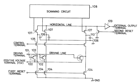
Fig. 1 is a circuit diagram of a photoelectric
transducer apparatus as a line sensor according to a
first embodiment of the present invention, and Fig.
2 is a timing chart for explaining the operation
thereof.
Referring to Figs. 1 and 2, capacitor electrodes
101 of photosensor cells 100 are commonly connected to
a driving line, and collector electrodes 102 thereof
are commonly connected to a positive voltage terminal.
A driving terminal is connected to the driving
11- 1338250
1 line.
A pulse signal is applied to the driving
terminal to drive the photosensor cells 100. Emitter
terminals 103 of the photosensor cells 100 are connected
to vertical signal lines and commonly connected to each
other through reset FETs 104. The emitter terminals
103 are connected to a ground terminal GND.
The gate electrodes of the FETs 104 are commonly
connected to a first reset terminal.
The FETs 104 are switching field effect tran-
sistors.
The vertical signal lines are connected to
store capacitors 106 through FETs 105 and to the
source electrodes of FETs 107. The drain electrodes
of the FETs 107 are commonly connected to a horizontal
signal line. The gate electrodes of the FETs 105 are
commonly connected to a control terminal.
The gate electrodes of the FETs 107 are
respectively connected to output terminals of a
scanning circuit 108.
Horizontal signal lines are connected to an
external output terminal through an output amplifier
109 and to the ground terminal GND through an FET 100.
The gate terminal of the FET 110 is connected
to a second reset terminal.
The FET 110 is a field effect transistor for
resetting the horizontal line.
1338250
- 12 -
1 The operation of the circuit in Fig. 1 will
be described with reference to a timing chart in
Fig. 2.
The control and first reset terminals are
simultaneously set at H level during the reset time.
During the reset time, the optical information stored
in the store capacitors 106 is discharged through the
FETs 104.
When the control terminal is set at H level
and the first reset terminal is set at L level, the
optical information stored in the photosensor cells
100 is read out onto the vertical signal lines by
applying the readout pulse signal to the driving
terminal. Therefore,~ the optical information is
stored in the store capacitors 106.
In this manner, when the readout pulse signal
is set at H level, readout operation of the photo-
sensor cells 100 is started. After the lapse of a
predetermined period of time, the readout pulse signal
is set at L level, thereby terminating the readout
operation.
When the control terminal is set at L level,
and the first reset and driving terminals are set at
H level, the refresh operation state is obtained.
The optical information stored in the photosensor
cells 100 is erased through the FETs 104.
When the refresh pulse signal is set at L
_ - 13 -
1338250
l level, the refresh operation is ended.
Thereafter, during the period until the
readout operation state is obtained again, the store
time for storing the carriers in the photosensor cells
100 is defined.
The signal pulses from the output terminals
of the scanning circuit 108 are used to sequentially
turn on the FETs 107 according to the shift timings.
The optical information signals stored in the
store capacitors 106 are sequentially read out onto
the horizontal lines by horizontal scanning of the
scanning circuit 108. The readout signals are amplified
by the output amplifier 109 and appear at the external
output terminal.
15When all optical information signals stored in
the store capacitors 106 are read out completely, the
reset time is initialized again.
The above operations are thus repeated.
With the above arrangement, the signal charge
is not kept on the vertical signal line for a long
period of time, thus reducing blooming and smearing.
A second embodiment of the present invention
will be described with reference to the accompanying
drawings.
25Fig. 3 is a circuit diagram of a photoelectric
transducer apparatus according to the second embodiment.
_ - 14 - 13382~0
1 Referring to Fig. 3, photosensor cells 1 as
the photoelectric transducer elements are one-
dimensionally arranged.
Capacitor electrodes 2 of the photosensor
cells 1 are commonly connected to a driving line and
to a driving terminal. Collector electrodes 3 of the
photosensor cells 1 are commonly connected to a positive
voltage terminal.
Emitter electrodes 4 of the photosensor cells
1 are respectively connected to vertical lines 5.
The vertical lines 5 are commonly connected through
FETs 6. The FETs 6 are connected to a ground terminal
7.
The gate electrodes of the FETs 6 are commonly
connected to a first reset terminal.
The capacitors 9 and the source electrodes of
the FETs 100 are respectively connected to the vertical
lines 5 through FETs 8. The capacitors 9 are connected
to a ground terminal 12 through a ground line 11.
The capacitors 9 are signal charge store
capacitors, respectively.
The gate electrodes of the FETs 10 are
respectively connected to output terminals 14 of the
scanning circuit 13. The drain electrodes of the
FETs 10 are connected to an output amplifier 16
through a horizontal line 15. The output terminal
of the output amplifier 16 is connected to an external
- 15 - 1338250
1 output terminal 17, so that an output voltage is
extracted from the external output terminal 17.
The gate electrodes of the FETs 10 are
respectively connected to the gate electrodes of
FETs 18. The drain electrodes of the FETs 18 are
connected to an output amplifier 20 through an output
line 19.
The output terminal of the output amplifier 20
is connected to an external output terminal 21, so that
an output voltage is extracted from the external output
terminal 21.
The source electrodes of the FETs 18 are
connected to the vertical lines 5 through FETs 22.
In the abov:e-embodiment, one electrode of each
of capacitors 24 is connected between a corresponding
one of the source electrodes of the FETs 18 and a
corresponding one of the FETs 22 through a corres-
ponding one of vertical lines 23. The other electrode
of each of the capacitors 24 is connected to the ground
line 11,
The capacitors 24 serve as dark voltage store
capacitors, respectively. Reset FETs 26 are connected
between the lines 15 and 19 and ground, respectively.
The gate electrodes of the FETs 26 are connected to
the second reset terminal. A control circuit 27
supplies timing pulses (Fig. 4) to the respective
terminals.
- 16 - 1338250
1 The operation of the above embodiment will be
described below.
As shown in the timing chart of Fig. 4, the
photosensor cells store optical information corres-
ponding to the amounts of light upon light storeoperation during the light irradiation store time.
During a predetermined period of time until
the llght information readout, the photosensor cells
1 perform store operations of carriers upon light
irradiation. During the reset time, both the control
and first reset terminals are set at H level, so that
the charges stored in the capacitors 9 are reset
through the corresponding FETs 6.
The control-t-erminal is set at H level, and
the first reset terminal is set at L level. When a
readout pulse voltage is applied to the driving
- terminal, the optical or light information stored in
the photosensor cells 1 is read out onto the vertical
lines, and the light information is stored in the
capacitors 9.
When the light information readout time has
elapsed, the first reset terminal is set at H level
and the control terminal is set at L level. In this
state, when the refresh pulse voltage is applied to
the driving terminal, the photosensor cells 1 are
maintained in the refresh state. The light informa-
tion stored in the photosensor cells 1 is erased
- 17 - 1338250
1 through the FETs 6.
When the refresh time has elapsed, the photo-
sensor cells 1 are temporarily shielded from light so
that a shading time is started.
In this case, the photosensor cells 1 store the
dark voltage generated in the dark state. It should be
noted that the dark voltage store time is controlled
to be equal to the light irradiation store time.
Subsequently, both the dark voltage readout
terminal and the first reset terminal are set at H
level to reset through the FETs 6 the charges stored
in the capacitors 24 during the reset time.
The light information corresponding to the
dark voltage components stored in the photosensor
cells 1 is read out onto the vertical lines under
the following conditions. The dark voltage readout
terminal is set at H level, the first reset terminal
is set at L level, and the readout pulse voltage Er
is applied to the driving terminal. Therefore, the
dark voltage signals are stored in the corresponding
capacitors 24.
When the dark voltage readout time has
elapsed, the dark voltage readout terminal is set at
L level, and the first reset terminal is set at H
level. The refresh pulse voltage E0 is applied to
the driving terminal to set the photosensor cells 1
in the refresh state.
- 18 - 13382~0
l When a predetermined period of time has
elapsed, the refresh pulse voltage applied to the
driving terminal is set at L level. Therefore, the
refresh time is terminated. Along with this, the
shading time is ended, and the first reset terminal
is set at L level.
Subsequently, clocks are supplied to the
- scanning circuit 13 to sequentially shift the output
pulses from the output terminals 14 thereof. The
FETs 10 and 18 are sequentially turned on in response
to these timing pulses.
By this horizontal scanning, light information
signals are sequentially read out from the capacitors
9 onto the horizont-a~ line 15. In synchronism with
the readout operation, the information signals corres-
ponding to the dark voltage components stored in
the capacitors 24 are read out onto the output line l9.
In this manner, the light information signals
read out onto the horizontal line 15 are output to
the external output terminal 17 through the output
amplifier 16. The information signals corresponding
to the dark voltage components read out onto the
output line 19 are output to the external output
terminal 21 through the output amplifier 20, so that
the output voltage is thus extracted from this external
output terminal.
For example, the readout operation for one
` ~ - 19 - 1338250
1 horizontal scanning time is completed, and the reset
time is started. Thereafter, the above operations
will be repeated.
Since the photoelectric transducer apparatus
of this embodiment is operated as described above,
an additional external circuit which was required
in the conventional photoelectric transducer apparatus
to remove the noise component caused by the dark
voltage need not be used, thereby smplifying the
system configuration. Therefore, demand for a low-
cost photoelectric transducer apparatus can be
satisfied.
In the above embodiment, the actual light
information signals simultaneously read out onto
lS the corresponding lines and the information signals
corresponding to the dark voltage components are
amplified by the output amplifiers 16 and 20 in an
output circuit 25, and the amplified signals are
extracted through the external output terminals,
respectively. However, the present invention is
not limited to the above arrangement. As shown in
Fig. 3, (a third embodiment), the output circuit 25
may be replaced with a differential amplifier 28 to
subtract the information corresponding to the dark
voltage components from the actual light information.
Light information representing a difference may be
output from a terminal 29.
_ - 20 - 1 ~ 3 8 2 5 0
1 In the second and third embodiments, the dark
voltage store time is set to be equal to the light
irradiation time. However, such setting need not be
performed.
For example, by effectively utilizing the
relationship between the dark voltage store time and
the amount of dark voltage components generated by
the photosensor cells 1, i.e., a substantially pro-
portional relationship, the dark voltage store time
may be set to be shorter than the light irradiation
time, and gains of the output amplifiers 16 and 20
in the output circuit 25 may be independently
controlled. Alternatively, the capacitances of the
store capacitors 9-and 24 are adjusted to obtain the
same effect as in the above embodiments.
In the second and third embodiments, the
photosensor cells are one-dimensionally aligned.
However, the arrangement of the cells is not limited
to this.
As described above, the photoelectric
transducer apparatus comprises light information
storing means for storing light information read out
from the photoelectric transducer element, and dark
voltage storing means for storing a voltage corres-
ponding to the dark voltage component read out from
the photoelectric transducer element. The actual
light information stored in the light information
- 21 - 13382SO
l storing means and the information corresponding to
the dark voltage component stored in the dark voltage
storing means are simultaneously read out from the
separate output lines. Therefore, the information
corresponding to the dark voltage included in the
output can be corrected in units of photosensor
cells when the actual optical information read out
from the photosensor cell is output, and noise caused
by variations in dark voltage can be removed from
the output signal. Unlike in the conventional photo-
electric transducer apparatus, an additional external
circuit is not required to simplify the system configu-
ration. In addition, demand for an economical
photoelectric trans-ducer apparatus can be satisfied.
A fourth embodiment of the present invention
will be described in detail with reference to the
accompanying drawings.
Fig. 5 is a circuit diagram of photoelectric
transducer elements arranged in a 4 x 4 matrix to
constitute a photoelectric transducer apparatus.
The photoelectric transducer apparatus
includes: basic photosensor cells 100 (the collector
of each bipolar transistor is connected to the sub-
strate and the substrate electrode), horizontal
lines 31, 31', 31", and 31'" serving as the readout-
refresh pulse lines; a vertical shift register 32
for generating a readout pulse; buffer MOS transistors
~ - 22 - 13~82~0
1 33, 33', 33", and 33'" arranged between the vertical
shift register 32 and the horizontal lines 31, 31',
31", 31'"; a terminal 34 for applying a pulse ~R to
the drains of the buffer MOS transistors 33, 33', 33",
and 33'"; a vertical shift register 32' for generating
a refresh pulse; buffer MOS transistors, 47, 47', 47",
and 47'" formed between the vertical shift register
32' and the horizontal lines 31, 31', 31~, and 31'";
a terminal 48 for applying a pulse to the drains of
the buffer MOS transistors 47, 47', 47", and 47'";
vertical lines 35, 35', 35", and 35'" serving as
vertical readout lines for reading out signal charges
from the basic photosensor cells 100; capacitors
37-1, 37-2, 37-1',-37-2', 37-1", 37-2", 37-1'",
and 37-2'" for storing these signal charges;
transfer MOS transistors 36-1, 36-2, 36-1', 36-2',
36-1", 36-2", 36-1"', and 36-2'" arranged between
the vertical lines 35, 35', 35", and 35'" and the
capacitors 37-1, 37-2, 37-1', 37-2', 37-1", 37-2",
37-1'", and 37-2'"; a horizontal shift register
46 for generating a pulse for selecting each store
capacitor; gate MOS transistors 38-1, 38-2, 38-1',
38-2', 38-1", 38-2", 38-1'", and 38-2'" for charging/
discharging the store capacitors 37-l, 37-2, 37-1',
37-2', 37-1", 37-2", 37-1'", and 37-2'"; output
lines 39-1 and 39-2 for reading out the store voltages
and supplying them to an amplifier; MOS transistors
- 23 - 1338250
1 40-1 and 40-2 for refreshing the charges on the readout
lines; a terminal 41 for applying the refresh pulse
to the MOS transistors 40-1 and 40-2; transistors
42-1 and 42-2 such as bipolar transistors, MOSFETs
or JFETs for amplifying the output signals; output
terminals 43-1 and 43-2 of the transistors 42-1 and
42-2; MOS transistors 44, 44', 44", and 44'" for
refreshing the charges stored on the vertical lines
35, 35', 35", and 35'"; a terminal 45 for supplying
a pulse to the gates of the MOS transistors 44, 44',
44", and 44'"; a horizontal shift register 46 for
turning on the MOS transistors 38-1, 38-2, 38-1',
38-2', 38-1", 38-2", 38-1'", and 38-2'"; and a
control circuit 200-for supplying signals to the
respective terminals.
The operation of the photoelectric transducer
apparatus will be described with reference to Fig. 5
and a timing chart of Fig. 6.
Assume that the collector potential of the
photosensor cells is kept at a positive potential
in the following description.
The store operation is performed until the
tl, and holes corresponding to the amounts of light
incident on the photoelectric transducer cells 100
are respectively stored in their p-type base regions.
At time tl, a pulse signal ~vc rises to turn
on the transistors 44, 44', 44", and 44'". A pulse
~ - 24 - 1 33 82 5 0
l signal ~Tl rises to turn on the transistors 36-1,
36-1', 36-1", and 36-l'" to refresh the store capacitors
37-1, 37-1', 37-1", and 37-1'". A pulse signal ~Hc
rises to turn on the transistors 40-1 and 40-2 to
refresh the residual charges on the output lines
39-1 and 39-2. Subsequently, the pulse signal vc
falls to turn off the transistors 44, 44', 44", and
44'", and the vertical lines 35, 35', 35", and 35'"
and the capacitors 37-1, 37-1', 37-1", and 37-1'"
are set in the floating state. A pulse signal ~vl
is output from the vertical shift register 32 to
turn on the transistor 33. When a readout pulse
signal ~R is then applied to the terminal 34 and
to the horizontal iine 31 through the transistor
33, the readout operation of the photoelectric
transducer cells 100 of the first row is started.
By this readout operation, the readout signals from
the cells of the first row appear on the vertical
lines 35, 35', 35", and 35'" and in the store
capacitors 37-1, 37-1', 37-1", and 37-1'". When
the readout operation is completed, the pulse signal
~T1 falls to turn off the transistors 36-1, 36-1',
36-1", and 36-1'". The capacitors 37-1, 37-1',
37-1", and 37-1'" and the vertical lines 35, 35',
35", and 35'" are disconnected, and then the residual
charges on the vertical lines 35, 35', 35", and 35'"
are refreshed.
_ - 25 - 1 33 825 0
1At time t2, a pulse signal ~ T2 rises to turn
on the transistors 36-2, 36-2', 36-2", and 36-2'" so
that the charges in the store capacitors 37-2, 37-2',
37-2", and 37-2'" are refreshed. Subsequently, the
pulse signal ~vc falls to turn off the transistors
44, 44', 44", and 44'". A pulse signal ~v2 is output
from the vertical shift register 33', and the readout
pulse signal ~R is supplied to the horizontal line 31'
through the terminal 34. In this state, the readout
operation of the photoelectric transducer cells 100
of the second row is started. By this readout
operation, the readout signals from the cells 100 of
the second row appear on the vertical lines 35, 35',
35", and 35'" and fn the store capacitors 37-2, 37-2',
37-2", and 37-2'". Upon completion of the readout
operation for the second row, the pulse signal T2
falls to turn off the transistors 36-2, 36-2', 36-2",
and 36-2'", and the capacitors 37-2, 37-2', 37-2",
and 37-2'" and the lines 35, 35', 35", and 35'" are
disconnected. The pulse signal ~vc rises to refresh
the residual charges from the vertical lines 35, 35',
35", and 35'".
At time t3, the pulse signal ~Hc falls to
turn off the transistors 40-1 and 40-2. The pulse
signal ~Hl is output from the horizontal shift
register 46 to turn on the transistors 38-1 and
38-2. The charges in the capacitors 37-1 and 37-2
` 1338250
- 26 -
1 are amplified by the transistors 42-1 and 42-2 through
the transistors 38-1 and 38-2 and the output lines
39-1 and 39-2. The amplified signals appear at the
terminals 43-1 and 43-2. When this output operation
is completed, the pulse signal ~Hc rises to refresh
the output lines 39-1 and 39-2. Sub-sequently, the
pulse signals ~H2 and ~H3 are sequentially output
from the horizontal shift register 46. In the same
manner as described above, the readout signals from
the cell of the first row and the secoond column and
the cell of the second row and the second column and
the readout signals from the cell of the first row and
the third column and the cell of the second row and the
third column are sequentially output from the terminals
43-1 and 43-2. Every time the readout signals appear,
the output lines 39-1 and 39-2 are refreshed.
At time t4, a pulse signal ~cl is output from
the vertical shift register 32' to turn on the trans-
sistors 47 and 47'. A pulse signal ~F is applied to
the terminal 48 so that the refresh pulse is applied
to the horizontal lines 31 and 31' through the
transistors 31 and 31'. As a result, the refresh
operation of the photoelectric transducer cells
100 of the first and second rows is performed.
~_ - 27 - 13382~0
1 The readout and refresh operations for the cells
100 of the third and fourth rows are performed at time
tS in the same manner as in the cells of the first and
second rows. The readout and refresh operations are
repeated for the cells 100 of the first and second
rows at time t6. The above operations are repeated.
In the above operation, the time required
for sending the readout signal onto the vertical line
is the period between rising of the pulse signal ~R
and falling of the pulse signal ~Tl, i.e., between
the times tl and t2 when the output from the photo-
electric transducer cell 100 of the first row and
the first column is assumed. This time interval
apparently has a large margin. In the conventional
photoelectric transducer apparatus applied in the
video camera, the vertical line selected last by
horizontal scanning stores the signal charge for
about 52.5 ~s. For example, if the time interval
between rising of the pulse signal ~R and falling
of the pulse signal ~Tl is set to be 0.5 ~s, the
apparatus of this embodiment can be improved by
about 105 times (40 dB) for blooming and smearing,
as compared with the conventional apparatus.
Since the store capacitors are arranged, the
photosensitive transducer cells are disconnected
from the store capacitors by turning off the tran-
sistors 36-1, 36-2, 36-1', 36-2', 36-1", 36-2",
`` 1338250
_ - 28 -
1 36-1'", and 36-2'" after the signal charges are stored
in the store capacitors, the photoelectric transducer
cells 100 can be sufficiently refreshed. For example,
the refresh time may be a time interval between times
t3 and t5, i.e., one horizontal scanning cycle.
Therefore, the after image phenomenon can be reduced
as compared with the conventional case.
If the photoelectric transducer apparatus is
applied to a color video camera and color filters are
formed on the sensor cells, the number of capacitors
is that of the colors of column cells, and the opera-
tion as described above is performed. In this case,
only one vertical line is used for each column, and
the aperture of the sensor cells is not reduced.
lS For example, as shown in Fig. 5, the color filters
R, G, and B are arranged according to the Bayer's
scheme, and the cells are operated at the timings
shown in Fig. 6. B signals are stored in the
capacitors 37-1 and 37-1", G signals are stored in
the capacitors 37-2, 37-1', 37-2", and 37-1'", and
R signals are stored in the capacitors 37-2' and
37-2'", respectively.
In the above embodiment, the two vertical
lines are simultaneously accessed. However, the
number of lines is not limited to two, but can be
extended to three or more. In this case, the number
of store capacitors is that of vertical pixels which
~ - 29 - 13~82SO
1 are simultaneously accessed.
Fig. 7 is a circuit diagram showing a fifth
embodiment of the present invention. A decoder 49
is arranged between a vertical shift register 32
and horizontal lines 31, 31', 31", and 31'", and
a control circuit 200 is operated at timings shown
in Fig. 8.
In this embodiment, the decoder 49 also serves
the function of the photoelectric transducer cell
refresh vertical register 46 of the fourth embodiment
(Fig. 5), thereby further simplifying the system
configuration.
The operation of the fifth embodiment will be
described with reference to the timing chart of Fig.
8. Assume that the store operaiton is performed until
time tl, and that the holes corresponding to the amounts
of light incident on the photoelectric transducer cells
100 are respectively stored in their p-type base regions.
At time tl, a pulse signal ~vc has already
risen, the vertical lines have already been grounded,
and a pulse signal ~T1 rises to refresh the charges
of the capacitors 37-1, 37-1', 37-1", and 37-1"'.
Thereafter, when the pulse signal ~vc falls to set
the vertical lines and the capacitors in the floating
state, the decoder 49 outputs a pulse ~D1.
The signals from the photoelectric transducer
cells 100 of the first row appear on the vertical
- 30 - 13382~0
1 lines and in the capacitors 37-1, 37-1', 37-1", and
37-1'". After the readout operation is completed,
the pulse signal ~T1 falls to disconnect the capacitors
37-1, 37-1', 37-1", and 37-1'" from the vertical lines,
and the pulse signal ~vc rises again to refresh the
vertical lines. The pulse signal ~T2 rises to refresh
the capacitors 37-2, 37-2', 37-2", and 37-2'", and
the pulse signal ~vc then falls. When the pulse
signal ~D2 rises again, the signals from the photo-
electric transducer cells of the second row appearon the vertical lines and the-capacitors 37-2, 37-2',
37-2", and 37-2'". Thereafter, the pulse signal ~T2
falls and the pulse signal ~vc rises to refresh the
vertical lines. I~n this state, the signals from the
first row are stored in the capacitors 37-1, 37-1',
37-1", and 37-1'", and the signals from the second
row are stored in the capacitors 37-2, 37-2', 37-2",
and 37-2'".
In the same manner as in the first embodiment,
these stored signals are sequentially read out from
time t3 to time tS. In this case, during the time
interval from time t4 to time immediately before
time t5, the pulse signals ~D1 and ~D2 are set at
high level, so that the photoelectric transducer
cells 100 of the first and second rows are refreshed.
The readout and refresh operations of the
photoelectric transducer cells of the third and
~ - 31 - 1338250
1 fourth rows are performed in the same manner as
described above.
According to this embodiment, the refresh and
readout operations of the photoelectric transducer
cells of each cell are performed by using a single
vertical shift register, thereby simplifying the
system configuration.
In the above embodiment, the two output lines
are used. However, the number of output lines may be
three or more. For example, as shown in a sixth
embodiment of Fig. 9, four output lines are used in
units of colors of filters. In this case, the load
of the output lines can be reduced into 1/2 of the
two output lines. -In addition, an image processing
circuit can also be simplified.
The arrangement of Fig. 9 is different from
that of Fig. 5 in the following points. Output lines
39-3 and 39-4 are added. Transistors 38-l and 38-1'"
are connected to a transistor 39-3 instead of the
transistor 39-1. Transistors 38-2' and 38-2'" are
connected to a transistor 39-4 instead of the
transistor 39-2. Transistors 40-3 and 40-4, the
gates of which are commonly connected to the gates
of transistors 40-1 and 40-2, are added to refresh
the output lines 39-3 and 39-4. A transistor 42-3
for outputting a signal from the output signal 39-3,
an output terminal 43-4, a transistor 42-4 for
~ - 32 - 133 825 0
1 outputting a signal from the output line 39-4, and
an output terminal 43-4 are added.
Other arrangements of Fig. 9 are the same as
those of Fig. 5, and the same reference numerals as
in Fig. 5 denote the same parts in Fig. 9.
In the photoelectric transducer apparatuses
in the foruth to sixth embodiments as described above
in detail, a plurality of capacitors are arranged for
each readout line of the photoelectric transducer
cells. The signal charges can be stored in the
capacitors in a short period of time, and then the
readout lines can be disconnected therefrom. Therefore,
blooming and smearing caused by the present of the
signal charges on the-readout lines can be completely
Prevente.1.
Furthermore, since the refresh time can be
sufficiently prolonged, the after image phenomenon
can be effectively prevented.
Many lines are often simultaneously accessed
when the photoelectric transducer apparatus is applied
to a color video camera or the like. The capacitors
corresponding to the pixels to be accessed are arranged
for each readout line. The number of readout lines
need not be increased, and thus the aperture can be
increased. -
A seventh embodiment of the present inventionwill be described below.
1338250
1 Fig. 10 is a circuit diagram of a photoelectric
transducer apparatus according to the seventh embodi-
ment of the present invention.
Referring to Fig. 10, a driving pulse ~R is
applied from a control circuit 200 to capacitor
electrodes of photoelectric transducer cells S1 to
Sn. A predetermined positive voltage is applied to
the collector electrodes of the cells S1 to Sn. The
emitter electrodes of the cells S1 to Sn are res-
pectively connected to vertical lines VL1 to VLn.Each of these vertical lines is connected to one
terminal of a corresponding one of store capacitors
C1 to Cn (each having a capacitance Ct) through a
corresponding one of transistors Qtl to Qtn. The
other terminal of each of the capacitors C1 to Cn
properly receives a bias voltage Vct in a manner
to be described later.
One terminal of each of the capacitors Cl to
Cn is connected to an output line 201 through a
corresponding one of transistors QS1 and QSn. The
output line 201 has a stray capacitance Ch equal to
the capacitance Ct of each of the store capacitors
C1 to Cn.
The input terminal of an output amplifier 202
is connected to the output line 201 and to a transistor
Qrh for properly applying a reset voltage Vrh. The
value of the reset voltage Vrh is selected within the
- 34 - 133 82~
1 range wherein the linearity of the output amplifier
202 is not degraded. In this embodiment, the range
is l.5 to 3.5 V. The output amplifier 202 is connected
to a single power source and is driven thereby.
Pulses ~hl to ~hn are sequentially applied
from a scanning circuit 103 to the gate electrodes
of the transistors QSl and QSn. A pulse ~t is applied
to the gate electrodes of the transistors Qtl to Qtn.
A voltage Vvc is applied to the respective
vertical lines through transistors Qrl to Qrn. The
gate electrodes of these transistors receive a pulse
~vc. A control circuit 200 supplies a driving pulse
of each terminal. Fig. ll is a timing chart for
explaining the operation of the control circuit.
The transistors Qrl to Qrn and the transistors
Qtl to Qtn are turned on in response to the pulses ~vc
and ~t, respectively, to clear (duration Tl) the
capacitors Cl to Cn. Subsequently, the pulse ~vc is
set at L level, and the capacitors Cl to Cn are charged
(duration T2) with the readout signals from the photo-
electric transducer cells in response to the driving
pulse ~r. In this case, the bias voltage Vct is the
ground potential.
After the bias voltage Vct is set to be +2V,
the signals from the capacitors Cl to Cn are output
at timings of the shift pulses ~hl to ~hn.
More specifically, the transistor QSl is
~ _ 35 _ 13382~0
1 turned on in response to the pulse ~hl. As described
above, the signal read out from the photoelectric
transducer cell S1 and stored in the capacitor Cl
is read out onto the output line 201. Subsequently,
the transistor Qrh is turned on in response to the
pulse ~rh, and the output line 201 is reset to the
reset voltage Vrh (e.g., +2V). In the same manner
as described above, the readout signals stored in the
capacitors C2 to Cn are sequentially read out onto the
output line 101 and are output through the output
amplifier 102 (a duration T3).
When the output operation is completed, the
refresh operation is performed in response to the
pulse ~vc and the d~iving pulse ~ r (a duration T4).
The basic operation of the circuit in Fig. 10
will be described below.
Fig. 12 A is a circuit diagram for explaining
the basic operation of the circuit in Fig. 10, and
Fig. 12 B is a timing chart showing the voltage
waveforms.
Referring to Fig. 12 A , a switch for selecting
the ground voltage (contact A) or the bias voltage of
+2V (contact B) is equivalently connected to the store
capacitor Ct. A switch Qrh for applying the reset
voltage Vrh (+2V) is equivalently connected to the
output line 201. Also assume that the voltage of
the capacitor Ct is vl, and that the voltage of the
- 36 - 1338250
1 output line 201 is v2.
The capacitor Ct is connected to the contact
A and grounded, and the readout signal from the sensor
is stored in the capacitor Ct. The capacitor Ct is
then connected to the contact B and receives the bias
voltage of +2V. The voltage of the capacitor Ct at
the time of zero level of the readout signal is set
to be equal to the reset voltage of the output line.
Subsequently, when the switch Qs is closed,
the 1/2 component of the signal of the voltage vl
appears on the output line 201 since-Ct = Ch. This
voltage is input as a voltage V2 to the output
amplifier 202. Closing of the switch Qrh causes
resetting of the output line 201 at the voltage of
+2V (Fig. 12 B ).
According to this embodiment, only the signal
component is input to the output amplifier 102, and
the input voltage does not greatly vary upon resetting.
The dynamic range of the output amplifier 202 can there-
fore be increased. The amplitude of the voltage Vrh or
Vct can have a large margin.
By setting the potential of the output line201 connected to the input terminal of the output
amplifier 202 at a low potential excluding the ground
potential, the Vss terminal of the output amplifier
202 can be grounded and a positive voltage (+5V in
this case) can be applied to the Vdd terminal thereof
~~ - 37 - 1338250
l by a single power source. (For example, if the reset
potential is zero, the negative and positive potentials
are respectively applied to the Vss and Vdd terminals,
and thus two power sources are required).
If the bias voltage of the capacitor Ct is
not changed, the potential of the output line 201
greatly varies between the reset potential Vrh and
the signal component potential of the readout signal.
The sensor signal is normally amplified to a proper
signal level by a signal processor (to be described
later). If the above unnecessary component is
generated, the circuit system is saturated since
the unnecessary component has a magnitude larger
than that of the signal component, thereby degrading
the signal component. However, according to the
above embodiment, the above problem does not occur.
If an output amplifier having a wide dynamic range
is arranged, it prevents use of a low-level driving
source and design of a compact imaging device.
However, according this embodiment, the wide dynamic
range of the amplifier 202 is not required, so that
a compact imaging device can be provided.
Now assume the charge/discharge time. A reset
potential portion of the output signal Vout can
sufficiently drive a load capacitance (a bonding
capacitance, a wiring capacitance, an input tran-
sistor capacitance, and the like) by a source current
_- 38 - 1 3 3 8 2 ~ 0
1 of a source follower circuit. However, the signal
component portion of the output signal becomes a sink
current of the source follower circuit. If an output
resistance is not sufficiently small, a discharge time
constant is increased to degrade linearity of a small
signal. A decrease in output resistance causes current
consumption loss. According to this embodiment, since
the dynamic range of the output amplifier can be
narrowed, this problem does not occur.
10In order to eliminate the unnecessary voltage
variation component, a sample/hold (S/H) circuit is
required. The relationship between a timing pulse
for the S/H circuit and the signal component is
very important. It-is desirable not to arrange the
S/H circuit to obtain good temperature characteris-
tics and the power source voltage characteristics.
However, if the S/H circuit is not arranged, the
blocking characteristic curve of a low-pass filter
becomes steep when the output signal is band-limited
thereby, and hence image quality is degraded. How-
ever, according to this embodiment, since the S/H
circuit need not be used, the apparatus of this
embodiment can be stably operated against temperature
and voltage variations.
25Fig. 13 shows a schematic arrangement of an
imaging device using the above embodiment.
Referring to Fig. 13, an imaging element 501
~ - 39 - 1338250
1 has the same arrangement as in the embodiment of Fig.
10. An output signal Vout from the imaging element
501 is gain-controlled by a signal processing circuit
502 and is output as a standard NTSC signal or the
like.
Various pulses ~ and the bias voltage Vct
for driving the imaging element 501 are generated by
a control circuit 200. The control circuit 200 is
operated under the control of the control unit 504.
In this case, the control circuit 200 also serves
as the switching means for properly applying the
bias voltage Vct. The control unit 504 controls
the gain or the like of the signal processing circuit
502 on the basis of the output from the imaging element
501 to control the amount of light incident on the
imaging element 501.
The bias voltage Vct applied to the store
capacitors C1 to Cn is supplied from the control
circuit 200. However, an internal power source 601
shown in Fig. 14, may be arranged. In this case,
the internal power source 601 is operated in response
to a control pulse ~ct from the control unit 504 to
generate the bias voltage Vct.
In the photoelectric transducer apparatus as
described in detail, a simple method of temporarily
changing the reference potential of the capacitors
in the readout mode is employed, so that only a
- - 1338250
1 single power source for the imaging driving voltage
can be used. As a result, the imaging device can be
made more compact at lower power consumption.