Note: Descriptions are shown in the official language in which they were submitted.
S P E C I F I C A T I O N
1 339nl 9
Title of the Invention
Process for preparing a superconducting thin film
Backqround of the Invention
Field of the invention
The present invention relates to a process for
preparing a thin film of superconductor. More particularly,
it relates to a process for depositing on a substrate a
superconducting thin film of a compound oxide havinq a higher
transition temperature of superconductivity which can be
used for Josephson Junctions devices or the like.
More particularly, the present invention relates to a
process for depositing a superconducting thin film of
K2NiF4-type oxides such as [La, Ba]2CuO4, [La, Sr]2CuO or
the like.
Brief description of the drawings
Figure 1 illustrates an example of a sputtering
apparatus which is used to carry out the process of the
present invention.
Figure 2 shows an illustrative cross section of an
embodiment of a mold used for powder molding,
Figure 3 shows an example of manufacturing steps used
in the powder molding technique,
Figure 4 is an illustration of a test sample for
determining the temperature dependency of the
superconducting thin film produced according to the present
invention. *
.
- 1 33901 9
Figure 5 is a graph showing the temperature dependency
of resistance of [La, Ba]2CuO4 thin films produced
according to Example 1 of the process of the present
invention and according to a comparative example,
respectively.
Figure 6 is a graph showing the temperature dependency
of resistance of [La, Sr~2CuO4 thin films produced
according to Example 2 of the process of the present
invention and according to a comparative example,
10 reSpeCtively.
Description of the related art
Superconductivity is a phenomenon in which the
electrical resistance becomes zero and hence can be utilized
to realize a variety of devices and apparatus which are
required to reduce consumption of electrical energy and
several ideas of its applications which utilize the
phenomenon of superconductivity have been proposed.
However, their actual usage have been restricted because
the phenomenon of superconductivity can be observed only at
very low cryogenic temperatures. Among known
superconducting materials, a group of materials having so-
called A-15 structure show rather higher Tc (critical
temperature of superconductivity) than others, but even the
- 1 3390 1 9
highest recorded Tc in the case of Nb3Ge did not exceed 23.2
K.
This means that liquefied helium (boiling point of 4.2
K) is the only known cryogen which can realize such very low
temperature of Tc. However, helium is not only a limited,
costly resource but also requires a large-scaled system for
liquefaction. Therefore, other superconducting materials
having higher Tc have been desired. But-no material which
exceeded the above mentioned Tc had been found in all the
studies conducted for the past ten years.
The possibility of existence of a new type of
superconducting materials having much higher Tc was revealed
by Bednorz and Muller, who discovered a new oxide type
superconductor in 1986 (Z. Phys. B64 (1986) 189).
These new oxide type superconducting materials are
[La, Ba]2CuO4 and [La, Sr]2CuO4 which are called K2NiF4-type
oxides having a crystal structure similar to Perovskite-type
superconducting oxides which have been known (see for example,
U.S. Patent No. 3,932,315). The R2NiF4-type oxides show Tc as
high as 30 to 30 K which are much higher than the known
superconducting materials and hence it becomes possible to use
liquefied hydrogen (b.p. = 20.4 K) or liquefied neon
(b.p. = 27.3 K) as a cryogen which causes them to exhibit
superconductivity. Particularly, hydrogen is an inexhaustible
resource except for danger of explosion.
1 33901 9
Conventional methods for producing superconducting
compounds or metal alloys may be classified into two
categories: (a) the powder sintering technique in which
starting materials are blended into a mixture which is then
sintered, and (b) the vapour deposition technique in which an
alloy or a compound is vaporized into the gaseous phase and
deposited or grown on a substrate.
Figure 3 shows a series of operations in the typical
powder above mentioned sintering process which includes the
following steps:
(1) uniformly mixing powders having a particle size of
several ~m such as BaCO3, La2CO3 or SrC03, and CuO,
(2) molding the powders in a mold,
(3) performing prelimin~ry sintering of the molded
material at 900 C for 12 hours,
(4) removing the sintered article from the mold and then
pulverizing the same again,
(5) press-molding the pulverized powder, and
(6) sintering (reaction-sintering) the press-molded
material at l,100 C for 2 hours.
The vapor deposition technique has been used for
producing a thin film of superconducting material such as
Nb3Ge and BaPb1xBix03. In the case of Nb3Ge, particles of Nb
and Ge are sputtered from several targets each consisting of
Nb and Ge, respectively, and are deposited onto a substrate
to form a film composed of Nb3Ge. Japanese patent laid-open
No. 56-109,924 published August 31, 1981 discloses a process for producing a
thin filrn of BaPbl xBix03 by means of a sputtering technique.
~-.
1 33901 q
However, the above mentioned new type superconducting
materials of K2NiF4-type oxides which have ~ust been
discovered have been studied and developed only in the form
of sintered bodies or as a bulk produced from powders which
have been previously press-molded. In other words,
heretofore, no studies of film-deposition techniques have been
conducted on these new type superconductors. Therefore, the
resultant superconducting bodies must have a bulk form which
is difficult to be utilized in the form of a thin film which
is required in the field of electrical devices or elements.
Therefore, an object of the present invention is to
provide a process which can change the K2NiF4-type
superconducting oxides into a thin film form.
Summary of the Invention
The present invention provides a process for preparing a
superconducting thin film composed of a compound oxide of La and Cu
and Sr or Ba on a substrate, by sputtering, characterized by the use of a targetcomposed of a powder mixture of oxides, carbonates, nitrates, and/or
sulfates of La, Cu and Sr or Ba, in that the substrate is heated at a
temperature between 200C and 1,200C during the sputtering, in that said
sputtering is effected in the presence of argon gas and oxygen gas, the partial
pressure of the oxygen gas being in a range between 10-6 and 5 x 10⁻² Torr,
and in that a bias voltage of less than 1,500 V is imposed on said substrate
during said sputtering.
Preferably, the thin film presents a composition corresponding to the
formula:
(Lal x, MX)2CUO~Y
inwhichO<x<1, O<y<4,andMisBaorSr.
S
1 33qO 1 9
The substrate may be selected from any materials which
are known and used in the field of the sputtering technique,
such as a single crystal of magnesia, strontium titanate,
beryllia, alumina, silicon, yttrium stabilized zirconia (YSZ)
or the like.
It is also preferable that, after the sputtering is
completed, the deposited thin film is heat-treated at a
temperature between 600 and 1 200C.
References to the "Periodic Table" in the present
application refer to the IUPAC version of the Table, in which
Group Ia includes the elements H, Li, Na, K, Rb, Cs and Fr,
Group IIa includes the elements Be, Ng, Ca, Sr, Ba and Ra,
Group IIIa includes the elements Sc, Y, La and Ac.
Now, an apparatus which can be used to realize the
abovementioned process according to the present invention will
be described with reference to attached drawings which are not
limitative of the present invention.
Description of the drawings
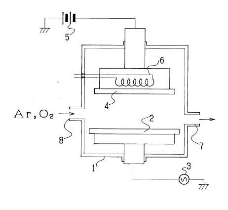
The apparatus illustrated in Figure 1 shows a sputtering
device including a sputtering material target 2 enclosed
~,
1 3390 1 9
in a vacuum chamber or bell jar 1 and a substrate 4 on
which the thin film is deposited facing to the
target 2. A vacuum pump (not shown) communicated through a
port 7 with the interior of the chamber 1 functions to
create vacuum therein. The target is impressed with high-
frequency electrical power from a high-frequency power source 3.
Bias voltage is impressed on the substrate 4 from a
source of high-voltage 5. The substrate 4 is heated by a
heater 6 so that the temperature of the substrate is
1~ adjustable. The bell jar 1 has a gas inlet 8 for
introducing argon gas and oxygen gas.
In operation, the target 2 is sputtered by Ar ions
in the presence of oxygen whose content or proportion is
adjusted so that additional oxygen is supplied to thethin
film which will be deposited on the substrate 4 to produce
a desired oxide.
Description of the Preferred Embodiments
In a preferable embodiment according to the present
invention, the target is in the form of a sintered body.
Namely, the target used in sputtering is made of a sintered
body which is produced by sintering a powder mixture of the
above mentioned compounds each cont~ining at least one of La,
said element M, and Cu.
In this case, it is preferable to use a target of a
sintered body which is made from a mixture of the compounds
wherein the proportions or atom ratios of La, said
1 339nl 9
element M, and Cu in the mixture are adjusted in such a manner
that the resulting thin film of compound oxide of La, said
element M, and Cu has a composition of
[La1_x, Mx]2cuo4-y
in which, M is an element selected from a group comprising
elements of the Ia, IIa and IIIa Groups of the Periodic Table,
and 0 ~ x < l and 0 ~ y < 4.
When Ba is used as the element M, the value of the x
in the abovementioned composition is preferably selected in
the range of 0.025 - x _ 0.12, while, when Sr is used
as the element M, the value of the x in the abovementioned
composition is preferably selected in the range of
0.09 _ x _ 0.2~.
The compounds may be selected from a group comprising
oxides of La, said element N, and Cu, carbonates of the
same, nitrates or sulfates of the same.
In an embodiment of the present invention, said
mixture of compounds may be a powder mixture of La2C03,
BaC03 or SrC03, and CuO. In this case, said powder mixture
is preferably a powder mixture composed of 70 to 9~ % by
weight of La2C03, 1 to 20 % by weight of BaC03 or SrC03,
and 1 to 30 % by weight o' CuO.
It is preferable that the sintering operation is
carrie~ out in a powder hot-press or in a hot isostatic
press (HIP).
The sputtering is preferably operated under the
presence of oxygen sas. The partial pressure of oxygen gas
1 33snl 9
is preferably adjusted to a range between 10-6 and
10-2 Torr. It is also preferable that the substrate on
which the thin film is deposited is heated to a temperature
between 100 and 1,200 C during sputtering~
It is also preferable that a bias voltage of lO to l,500 V
is impressed onto said substrate during sputtering
operation.
Another preferable feature of the present invention
resides in that, after the sputtering operation is completed,
the deposited thin film is heat-treated a~ a temperature
between 600 and 1,200 C.
The structure of the resulting thin film can be
proved to be a crystalline film having K2NiF4-type
layered perovskite structure by electron probe
microanalysis (EPMA) or X-ray diffraction.
According to a preferred embodiment of the present
invention, the process for preparing a superconducting thin
film composed of a compound oxide of La, one element M
selected from a group of Ia, IIa and IIIa elements in the
~C Periodic Table, and Cu by a sputtering technique is
characterized in that a target of a sintered body which is
made from a mixture of the compounds wherein the proportions
or atom ratios of La, said element M, and Cu in the mixture
are adjusted in such a manner that the resulting thin film of
compound oxide of Ja, said element M~ and Cu has a
composition of
[Lal_x, MX]2CUO4-Y
- 1 33snl 9
in which, M is an element selected from a group comprising
elements of the Ia, IIa and IIIa groups of the Periodic Table,
0 < x < 1 and 0 _ y < 4, and in that , after the
sputtering complete, the deposited thin film is heat-
treated at a temperature between 600 and 1,200 C in air.
According to another preferred embodiment of the
present invention, the process for preparing a
superconducting thin film composed of a compound oxide of
La, one element M selected from a group of Ia, IIa and IIIa
elements in the Periodic Table, and Cu by a sputtering
technique, is characterized in that a target of a sintered
body which is made from a mixture of the compounds wherein
the proportions or atom ratios of La, said element M, and
Cu in the mixture are adjusted in such a manner that the
resulting thin film of compound oxide of La, said element M,
and Cu has a composition of
[La1_x, MX]2CUO4-Y
in which, M is an element selected from a group comprising
elements of the Ia, IIa and IIIa groups of the Periodic Table,
2 r 0 < x < 1 and 0 _ y < ~, in that the substrate on which the
thin film is deposited is heated to a temperature between
100 and 1,200 C during sputtering operation, and in that,
after the sputtering is completed, the deposited thin film is
heat-treated at a temperature between 600 and 1,200 C in
air.
During the sputtering operation, argon gas contained
in the vacuum chamber is ionized into Ar+ and
1 339()l 9
is accelerated so that the Ar+ ions strike the target composed
of the material to be deposited as a film, resulting in that
particles sputtered out of the target are deposited on the
substrate in a form of a thin film. When the target is made
of a compound oxide made from La203, SrC03, and CuO or the
like, particles of each of the oxides are sputtered. If, at
this stage of the sputtering process, oxygen gas is introduced
into the vacuum chamber, a thin film of [La1x, Bax]2CuO4y or
[La1x, Srx]2CuO4y which is the most stable compound is
deposited on the substrate.
The composition of the thin film deposited on the
substrate depends on the composition of material of the
target. The present invention is based on such finding of the
present inventors. Thus, if the atom ratios of La, said
element M, Cu, and oxygen in the target are adjusted in such
manner that the resulting thin film of compound oxide of La,
said element N, and Cu has a composition of [La~x, Mx]2Cu04y,
(wherein M is an element selected from a group comprising
elements from the Ia, IIa and IIIa groups of the Periodic
Table, O < x < 1 and O ~ y < 4, a thin film of superconductor
having high-Tc can be produced. In other words, thin films
of superconductors having high-Tc and having R2NiF4-type
layered perovskite structure can be obtained by controlling
the proportions in the mixture of the target.
In a preferred embodiment, the sputtering is performed
-- 1 33901 9
by using a target which is a sintered body which is produced
by sintering powders of oxides, carbonates, nitrides or
sulfates each contAining at least one of La, Ba (or Sr), and
Cu which are constituent elements of the resultant
superconducting film having the K2NiF4-type oxide.
The R2NiF4-type compound oxide can be formed into a
film, since these oxides, carbonates, nitride and sulfates
are relatively stable.
According to a preferred embodiment, the sintered body
is made from powders of La203, BaC03 (or SrC03) and CuO
having such proportions as 70 to 95 % by weight of La2C03,
1 to 20 % by weight of BaC03 or SrC03, and 1 to 30 % by
weight of CuO.
Now, we will describe how to control proportions of
components in the thin film.
Table 1. shows melting points of the abovementioned
powder:
Material Melting point
La203 2,307 C
BaC03 1,740 C
SrC03 1,~97 C
CuO 1,326 C
It is apparent from Table 1 that La203 has a higher
melting point than the others and hence is considered to be
vaporized at a lower speed than the others during the
sputtering. This means that the desired proportions of
12
- 1 3390 1 9
elements in the thin film cannot be obtAine~ if the sintered
body does not have proper proportions of the elements.
According to the present invention, the target consisting
of a molded and sintered body contains an amount of
La203 which is larger than the desired stoichiometrical
proportion in the thin film. Namely, according to a
preferred embodiment, the target is composed of a sintered
body produced from a mixture of 70 to 90 % by weight of
La203, 1 to 20 ~ by weight of BaCO3 (or SrCO31) and 1 to
30 % by weight of CuO.
When the target is a mixture of La2CO3, BaCO3 and CuO
is used, a thin film of [La1_x, Bax]2CuO4-y is obtained,
while when the target is a mixture of La2co3l SrC03, and
CuO is used, a thin film of [La1-x, Srx]2cuo4-y is
obtained. The higher critical temperature is expected in a
range of 0.025 _ x _ 0.125 for [La1-x, BaX]2CUO4-y and
in a range of 0.09 _ x _ 0.25 for [La1-x~ Srx]2cuo4-y
respectively.
The composition of the thin film is not influenced
much by the existence of the abovementioned non-reacted
portions in the target but is rather influenced greatly by
the proportlon of powders in the mixture. In the
industrial scale, the powder sintering is preferably
carried out by hot pressing, hot isostatic pressing, or the
2c like.
According to another aspect Oc the present invention,
the sputtering is preferably conducted in an atmosphere of
- . l 33snl 9
oxygen gas in the presence of argon gas. The partial
pressure of the oxygen gas is preferably adjusted to a
range between 10-6 and 5 x 10⁻² Torr, more preferably
between 10-6 and 10-2 Torr.
According to still another aspect of the present
invention, the substrate on which the thin film is deposited
is preferably heated to a temperature between 100 and 1,200
C during sputtering. Also, a bias voltage of less than
500 V is preferably impressed onto the substrate during
sputtering operation to attract ionized oxygen towards the
substrate.
According to still another aspect of the present
invention, the deposited thin film is preferably heat-
treated at a temperature between 600 and 1,200 C, after
1 r the sputtering is completed.
In the case of K2NiF4-type oxides according to the present
invention, it is important that oxygen atoms are orderly
contained among the other constituent atoms. Therefore,
according to 2 preferred embodiment, the partial pressure
of oxygen is adjusted between 10-6 and 5 x 10⁻² Torr, more
preferably between 10-6 and 10-2 Torr~during the sputtering
in order to rationalize the amount of oxygen in the
resultant superconducting thin film. If the partial
pressure is lower than 15-6 Torr, no effect of addition of
2S oxygen is obtained because substantially no oxygen exist in
the atmosphere. However, if the partial pressure of
oxygen exceeds 5 x 10⁻² Torr, sputtering cannot be
14
1 3390 1 9
practiced since the vacuum pressure is too high. Therefore,
the partial pressure of oxygen must be within the range
between 10-6 and 5 x 10⁻² Torr, more preferably 10-6 Torr and
10-2 Torr. The sputtering may be high-frequency sputtering or
DC sputtering, but high-frequency sputtering is preferable.
In special cases, the thin film may be produced by the ion-
plating technique.
In the case of high-frequency sputtering, the applied
high-frequency power varies according to the sputtering
apparatus used but is preferably lower than 5,000 W. In fact,
if the power exceeds 5,000 W, excess energy is given to the
ions in the vacuum, which adversely results in an increase of
impurities produced from the walls of the chamber.
It is also possible to bias the substrate at a voltage
between 0 V and 1500 V, more preferably between 10 V and 1500
V, so that ionized oxygen are accelerated towards the
substrate. Higher voltages which exceed 1500 V should not be
used because abnormal discharge due to DC voltage will be
produced and because too many ions strike the thin film,
resulting in a great number of defects will be produced in the
film and hence the film will be deteriorated.
Further, when the temperature of the substrate is not
higher than 100 C, the thin film becomes amorphous and
does not exhibit superconductivity. To the contrary, if
the substrate is heated to a temperature higher
than 1,200 C, it is difficult to adjust the
- 1 33901 q
proportions of elements in the film. Therefore, the
temperature of the substrate is preferably within the range
of from 100 C to 1,200 C in air.
It is effective to heat the resulting superconducting
thin film obtained by the abovementioned film forming
process to a temperature between 600 and 1,200 C in air in
order to improve the superconductivity.
The resulting superconducting thin films obtained
according to the abovementioned process shows far higher
superconducting critical temperatures than existing
superconducting films and hence superconducting transitions
can be realized without using liquified helium.
Now, the process according to the present invention
will be described with reference to illustrative Examples,
but the scope of the present invention should not be
limited thereto.
Example 1 - Preparation of [La, Sr]2CuO4 thin film -
Powders of La2O3, SrC03 and CuO are mixed uniformly in
the proportion of 1.66 : 0.34 : 1 to prepare a target.
Then, the powder mixture is subjected to a preliminary
sintering at 900 C for 12 hours in a mold shown in Figure
2 in which 20 denotes the powders for the target and 22
denotes the mold.
The resulting molded article removed from the
mold is very fragile and is pulverized again. The
- ~ 16
- 1 3390 1 9
resulting pulverized powder is subjected to a final
sintering at 1,100 C for 2 hours.
A sintered body obtained by the procedure
above mentioned as a target is placed in the sputtering
apparatus shown in Figure l. Sputtering is performed under
such conditions that a surface of the substrate is maintained
at a temperature of 200 C and a high-frequency voltage of l
KV is applied to the substrate.
The resulting thin film is confirmed to be a
crystalline film having K2NiF4-type layered perovskite
structure by electron probe microanalysis ~EPMA).
After the thin film is annealed at 900 C, the
transition temperature or the critical temperature is
found to be higher than 30 R.
It is impossible to obtain a thin film consisting of a
compound of [La1_x, Srx]2cuo4-y and having higher
transition temperatures when the value of x does not fall
within the range of 0.09 _ x _ 0.25.
Example 2 - Preparation of [La, Ba]2CuO4 thin film -
[La, Ba]2CuO4 thin film is produced in a high-
frequency sputtering machine illustrated in Figure 1.
The target material is a sintered body made from a
powder mixture of La2O3, BaCO3 and CuO, while the substrate
4 is a silicon crystal. The film is produced under the
following conditions:
1 33~01 q
Partial pressure of Ar as sputtering gas 10~3 Torr
Partial pressure of oxygen 10~4 Torr
Temperature of the substrate 900 C
High-frequency power impressed to the target 500W
Substrate bias voltage 50 V
A thickness of about 1 ~m is obtained at a film-
forming speed of 10 A/sec. As a comparative example, the
same procedure is repeated except that oxygen is not
supplied.
A sample shown in Figure 4 is prepared from each
resulting substrate having a thin film thereon in order to
determine the resistance of the thin film. The sample for
resistance measurement shown in Figure 4 comprises the
substrate 4, a thin film 9 of [La, Ba]2CuO4 deposited on the
substrate, and two pairs of electrodes 10 made of aluminum
which are vacuum-deposited on a surface of the thin film 9.
Two pairs of lead wires 11 are soldered to the aluminum
electrodes 10 respectively.
Figu e ~ shows the temperature dependency of
resistance of the thin films measured on Example 1 and its
comparative example. In Figure 5, the curve expressed by the
solid line having a reference number 31 shows the
temperature dependency of the resistance of the thin film
which is produced in a bell jar containing oxygen whose
pa_tial pressure is 10~4 Torr, while the curve shown by
the dashed line having a reference number 32 shows that of
18
1 33901 9
another thin film which is produced in the bell jar into
which oxygen is not fed.
It is apparent from the curve of resistance 31 that the
thin film produced according to the process of the present
invention shows an onset temperature when the phenomenon
of superconductivity starts is about 30 K and complete
superconductivity is observed below 25 K, while the curve
of resistance 32 shows zero-resistance only below
several K and has a rather gentle slope although the
resistance starts to drop from nearly same temperature as
for the above case. Comparison between these two curves
reveals that introduction of oxygen gas into the bell jar
during the film deposition permits control or adjustment of
the oxygen content in the thin film to obtain a
superconductive thin film having a desired composition.
Example 3
- preparation of a thin film of [La, Sr]2CuO4 -
The same procedure as in Example 2 for [La, Ba]2CuO4
is repeated. As target material, a sintered body produced
from a powder mixture of La203, SrC03~ and CuO is used.
Fllms are deposited by using two different targets each
consisting of a sintered body produced from a powder
mixture containing 20 % and 60 % by weight of CuO
res?ectively.
The film is deposited under the following conditions:
1 9
1 33901 9
Partial pressure of Ar as sputtering gas 10~3 Torr
Partial pressure of oxygen 10~4 Torr
Temperature of the substrate 900 C
High-frequency power applied to the target 500W
Substrate bias voltage 50 V
Figure 6 shows the temperature dependency of
resistance of the resulting thin films, wherein the curve
expressed by the solid line having a reference number 4l
illustrates the curve of resistance of a thin film produced
lC by the first target containing 20 % by weight of CuO, while
the curve expressed by the dashed line having a
reference number ~2 illustrates that of another thin film
produced by the second target contAining 60% by weight of CuO.
It is apparent from the curve 42 that the thin film
produced from the second target containing 60 % by weight
of CuO does not show superconductivity, while the thin film
produced from the first target containing 20 % by weight of
CuO according to the present invention shows an onset
temperature of about 38 K and complete superconductivity is
observed below 27 K. Thus, the Lilm corresponding to the
curve of resistance 41 shows improved properties as a
superconductor,
, :_