Note: Descriptions are shown in the official language in which they were submitted.
SINGLE COMPARTMENT, SELF ERASING, ~ ~
S()LU T I ~N - PHA SE E LECT ROCH ROI~ I C DEV I CE S , 1~ 3 9 ~-J 2 L
SOLUTION~; FOR US~ THEREIN, AND USES THEE~EOF
T~:C~lNI (~AL F IE LD
The present invention relates to devices of
reversibly variable transmittance to electromagnetic
radiation, compositions for use as media of reversibly
variable transmittance in such devices, and use of such
devices in variable transmission light filters and
variable reflectance mirrors. More particularly, the
invelltion relates to single-compartment, self-erasing,
solution-phase electrochromic devices, solutions for use
ti~erein and uses thereof.
BACK~ROUNV OF TH~ I NVENTION
Several different types of devices are known
wherein transmittance to electromagnetic radiation can
be reversi~ly varied. Among such devices are those
wherein the transmittance is changed by thermochromic,
pnotocnromic, or electro-optic (e.g., liquid crystal,
dipolar suspension, electrophoretic, electrochromic)
means and wherein the variable transmittance is to
electromagnetic radiation that is at least partly in the
visible range (wavelength from 4200~ to 7000~).
Devlces of reversibly variable transmittance to
electromaynetic radiation have found application as the
variable transmittance element in variable transmittance
light-filters, variable reflectance mirrors, and display
devices which employ such light-filters or mirrors in
conveying information. These variable transmittance
llght filters have included windows. The variable
reflectance mirrors have included anti-glare rearview
mirrors for automotive vehiclès.
Devices of reversibly variable transmittance to
electromagnetic radiation, wherein the transmittance is
altered by electrochromic means, including
electrochemichromic devices, are described, for example,
133~321
by Chang, "Electrochromic and Electrochemichromic
Materials and Phenomena," in Non-emissive Electrooptic
Displays, A. Kmetz and ~. von Willisen, eds. Pergamon
Press, New York, New York 1976, pp. 155-196 (1976).
Electrochemichromic devices includes those wherein
electrochemical reactions occur in a solid film, involve
electroplating or occur entirely in solution. See
Chang, supra.
Numerous electrochemichromic devices are known
in the art. See, e.g., Manos, U.S. Patent
No. 3,451,741; Bredfeldt et al., U.S. Patent
No. 4,090,782, Shattuck and Sincerbox, ~.S. Patent
No. 4,093,358; Clecak et al., U.S. Patent No. 4,139,276,
Kissa et al., U.S. Patent No. 3,453,038, Rogers, U.S.
Patent Nos. 3,652,149, 3,774,988 and 3,873,185; and
Jones et al., U.S. Patent Nos. 3,282,157, 3,282,158,
3,282,160 and 3,283,656. Among these devices are
single-compartment, self-erasing, solution-phase
electrochromic devices. See, e.g., Manos, supra;
Bredfeldt et al.,
supra; Shattuck and Sincerbox, supra: and Clecak et al.,
supra.
In a single-compartment, self-erasing,
solution-phase electrochromic device, the intensity of
electromagnetic radiation is modulated by passing
through a solution held in the device in a compartment
which includes two electrodes. The two electrodes are
in contact with the solution. Between the electrodes,
there is no barrier, such as a semi-permeable membrane,
which would divide the solution compartment and prevent
some components in the solution from diffusing or
migrating from one electrode to the other. The solution
includes a solvent and at least one "anodic" compound
(which can be neutral or charged) and at least one
"cathodic" compound (which also can be neutral or
charged). The "anodic" compounds are electrochemically
oxidized and the "cathodic" compounds are
13~9~321
electrochemically reduced when a DC electrical potential
difference is impressed across the solution between the
electrodes. If none of the "anodic" compounds and
"cat~odic" compounds to be oxidized or reduced is
charged, prior to oxidation or reduction, respectively,
the solution will, and otherwise the solution may,
include inert, current-carrying electrolyte. The
electrocnemical properties of the solvent, inert,
current-carrying electrolyte, if any, anodic compounds,
cathodic compounds, and any other components that might
be present in the solution are preferably such that the
anodic and catnodic compounds are oxidized and reduced,
respectively, at a potential difference between the
electrodes which does not cause any significant
electrochemical or other changes in the other components
in the solution. The solution is fluid during operation
of the device, although it may be gelled or made highly
vlscous with a thickening agent. That the devices are
"solution-phase" means that all of the components in the
solution, including the anodic and cathodic compounds,
remain in solution during operation of the device with
the concomitant oxidation of anodic compounds and
reduction of cathodic compounds.
~eversible modulation of intensity of
electromagnetic radiation passing through a
single-compartment, self-erasing, solution-phase
electrochromic device can be accomplished because of
tnree factors related to operation of the device.
First, the molar extinction coefficients of the anodic
compounds and cathodic compounds in the solution of the
device, as a function of wavelength, change with their
electrochemical oxidation and reduction, respectively.
Generally, at least one of these compounds undergoes a
significant change in extinction coefficient at
wavelengths in the visible range upon the oxidation or
reduction; consequently, the solution and device change
color or change from dark to clear or clear to dark when
4 1 3 3 9 ~ 2 1
a potential difference is applied across the solution
between the electrodes. Second, in the solution, the
oxidized anodic compounds and reduced cathodic compounds
do not, to any significant extent, undergo degradative
reactions unimolecularly or with other compcnents.
Third, in the solution, the oxidized anodic compounds
react substantially only with the reduced cathodic
compounds to yield substantially only anodic compounds
and cathodic compounds in their forms and with their
properties prior to the oxidations and reductions,
respectively. These reactions of oxidized anodic
compounds with reduced cathodic compounds provide the
"self-erasing" feature to the device.
Heretofore, no single-compartment,
self-erasing, solution-phase electrochromic devices have
been known which have proven to be suitable for
commercial application as the component of reversibly
variable transmittance in variable transmittance light
filters or variable reflectance mirrors. For such
applications, the solution of variable transmittance
must be highly stable to cycling, at least several
thousands of times, from zero potential difference
between the electrodes to a potential difference between
the electrodes that is sufficient to cause significant
change in transmittance and then back to zero again. In
a typical device, the solution is held in a layer
between planar, parallel, spaced-apart, transparent
walls, on the inside surfaces of which (in contact with
the solution) are coated thin layers of transparent,
electrically conductive material which serve as
electrodes and through which passes electromagnetic
radiation whose intensity is reversibly modulated in the
device. It is advantageous to have the solution layer
as thin as possible, in order to minimize distortion of
light passing through, or passing into and reflecting
out of, a device, and to reduce to durations that are
acceptable for commercial applications the "response
1339.i~2 1
-- 5 --
time" required for the transmittance of a device to
achieve a new steady-state value when the potential
difference between the electrodes is changed. However,
for devices with thin solution layers, anodic and
cathodic electrochromic compounds must be found that, at
concentrations in the solution at which they remain
soluble, both at zero-potential e~uilibrium and when
oxidized (in the case of anodic compounds) and reduced
(in the case of cathodic compounds) when a potential
difference is applied between the electrodes, give rise
to sufficiently large changes in absorbance between
their zero-potential equilibrium states and their
"activated" (i.e., oxidized or reduced) states and at
the same time remain sufficiently stable to cycling to
provide a commercially practicable device. The present
invention addresses the need for solutions to make
commercially practicable single-compartment,
self-erasing, solution-phase electrochromic devices.
A useful feature in such devices, that has not
heretofore been available, is the capability to function
as a gray-scale device, i.e., to vary continuously and
rapidly in transmittance to light in the visible
wavelength range as a function of the potential
difference applied between the electrodes of the
device. Such a "gray-scale" device would find
application in a window, which would allow light of
constant intensity to pass through independently of the
intensity of the light reaching the window, and an
anti-glare rearview mirror in an automobile, that would
reflect light of acceptable intensity to the driver
regardless of the intensity of the glare-causing light
incident on the mirror from headlamps of automobiles
approaching the vehicle from behind. The present
invention provides gray-scaling capability in
single-compartment, self-erasing, solution-phase
electrochromic devices.
1339~21
A problem that has not heretofore been
recognized with solution-phase electrochromic devices is
seyregation, due to both migration and natural
convection of anodic and cathodic electrochromic
compounds. Particularly in devices that are operated
continuously for long periods (more than about
~ minutes) with the planar surface through which light
enters the device oriented vertically to the ground,
sucn segregation can cause annoying and troublesome
separation of color and reduction in speed of
self-erasing. The present invention addresses this
segregation problem.
Variable reflectance mirrors include a variable
transmittance component, which is a device which has a
transmittance to visible light which is reversibly
varied by thermochromic, photochromic, or electro-optic
means, and a reflection means, which is a highly
reflective surface (such as a silver layer) from which
liyht is reflected after passing through a medium of
reversibly variable transmittance in the variable
transmittance component. After reflecting from the
reflection means, the reflected light passes back
tnrouyh t~e medium of reversibly variable
transmittance. The medium of variable transmittance in
sucn mirrors is typically held, in the variabl
transmittance component, between two planar, parallel,
spaced-apart surfaces. At least one of these surfaces
is transparent to light, and light reflected by the
mlrror enters and leaves through this transparent
surface. A problem with such mirrors is the high
"residual" reflectivity, which is usually greater than
5%, of this transparent surface of the variable
transmittance component. For example, in an anti-glare
rearview mirror for an automobile, wherein elimination
of ihigh glare may require reduction of reflectivity
observed by the driver from all surfaces to as low as
about 5 to 7%, the high residual reflectivity of the
front surface of a typical mirror requires that the 9
transmittance of the medium of reversibly variable
transmittance in the mirror be capable of being made as
low as about 3%. Because it is difficult to achieve
such low transmittance with sufficient speed in
preferably thin devices of reversibly variable
transmittance, it would be advantageous to have variable
reflectance mirrors wherein these problems caused by
high residual reflectivity are avoided. The present
invention provides such mirrors.
SUMMARY OF THE INVENTION
The present invention provides solutions for
use as the medium of reversibly variable transmittance
to electromagnetic radiation, particularly light in the
visible range, in single-compartment, self-erasing,
solution-phase electrochromic devices.
The invention provides further such
electrochromic devices, wherein a solution of the
invention is the medium of reversibly variable
transmittance; variable transmission light filters and
variable reflectance mirrors, wherein the variable
transmittance component is a single-compartment,
self-erasing, solution-phase device according to the
invention; and display devices wherein information is
displayed by operation of variable transmission light
filters or variable reflectance mirrors according to the
lnVentiOn.
The solutions of the invention render
commercially practical the use of single-compartment,
self-erasing, solution-phase electrochromic devices and
variable transmission light filters, variable
reflectance mirrors and display devices employing such
filters and mirrors. The solutions of the invention are
unexpectedly highly stable to cycling of potential
differences between the electrodes in devices of the
invention.
In devices of the invention wherein the 1~ 3 9 ~ 21
solution layer is desirably thin, and with
concentrations of anodic and cathodic compounds in the
solution that are low enough that precipitation does not
occur and problems of segregation are substantially
reduced, and at potential differences between the
electrodes that are low enough to avoid significant
degradation of the solution, the solutions of the
invention darken to an unexpectedly high absorbance to
visible light with unexpectedly high speed once the
potential difference is applied and clear again with
unexpectedly high speed once the electrodes are
open-circuited or short-circuited. Advantageously,
reversal of the polarity of the electrodes of a device
of the invention is not required for clearing to occur
with sufficient speed for many practical applications.
F~rther, devices of the invention can advantageously be
operated as gray-scale devices.
In another aspect, the present invention
entails novel electrochromic compounds and combinations
of compounds for use in solutions of the invention.
In still another aspect, the invention includes
an improved variable reflectance mirror, wherein
variable reflectance is provided by thermochromic,
photochromic, or electro-optic means in a device of
variable transmittance to electromagnetic radiation. In
such an improved mirror of the invention, problems due
to residual reflectivity from a planar surface through
which light enters, and after reflecting from the
reflecting means, leaves the mirror are avoided by
displacing this planar surface at a slight angle to the
highly reflective planar surface of the mirror which is
its reflecting means. Thereby, a person viewing the
mirror need not see light due to residual reflectivity
simultaneously with light that is reflected from the
mirror's reflecting means.
1339iJ21
- 8a -
In particular, the invention provides a novel compound of the
formula
Rl7 R ,8
~o~
wherein R77, R78 and R79 are the same or different and are each
selected from the group consisting of alkyl of 1-6 carbon atoms.
in:vs
13'~2 ~
BRIEF DESCRIPTION OF THE DRAWINGS
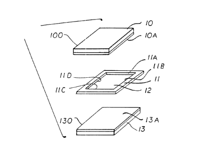
FIGURE 1 displays schematically an exploded
view of two planar, transparent, electrode-bearing
side6, 100 and 130, of a device of the invention
together with spacer or separating means, 11, which
holds the electrode-bearing sides apart and
substantially parallel in an assembled device of the
invention and the inside edges, llA, llB, llC and llD of
which, together with the electrode layers, lOA and 13A,
of the electrode-bearing sides, defines a space, 12,
which, in an assembled device of the invention, is
occupied by a solution according to the invention that
is in contact with the electrode layers.
FIGURE 2 illustrates schematically a partially
assembled device, 200, according to the invention.
FIGURE 2 shows, by cross-hatched area 14, the portion,
of planar, transparent side 100 of the device, which
overlays the solution of reversibly variable
transmittance in the device and which, consequently,
changes color, or changes from clear to dark and back,
as the device is operated.
FIGURE 3 illustrates schematically a view of a
cross-section of a partially assembled, improved
variable reflectance mirror, 300, according to the
invention, wherein the reflecting means is the highly
reflective layer 18A of a prism-shaped mirror, 180,
laminated to surface 131 of one transparent,
electrode-bearing side, 130, of a variable transmittance
device according to the invention.
FIGURE 4 illustrates schematically a view of a
cross-section of a partially assembled, improved
variable reflectance mirror, 400, according to the
invention, wherein the reflecting means is a high
reflectance layer, 20, on one electrode-bearing side,
130, of a variable transmittance device according to the
invention and a transparent prism-shaped object, 22, is
laminated to the surface 101 of the other
-- 10 --
electrode-bearing side, 100, of the variable 1~3~321
transmittance device according to the invention.
I)ETAIl,EI~ DESCRIPTION OF THE INVENTION
In one of its aspects, the present invention is
a solution, for use as the variable transmittance medium
in a single-compartment, self-erasing, solution-phase
electrochromic device, which comprises:
(A) a solvent;
(B) at least one cathodic electrochromic
compound which, in a voltammogram done with an inert
electrode in the solvent at room temperature, displays
at least two chemically reversible reduction waves, with
tne flrst of said reductions accompanied by an increase
in molar extinction coefficient at at least one
wavelengtn in the visible range;
(C) at least one anodic electrochromic
compound wnicll, in a voltammogram done with an inert
electrode in the solvent at room temperature, displays
at least two chemically reversible oxidation waves, with
the first of said oxidations accompanied by an increase
in molar extinction coefficient at at least one
wavelength in the visible range; and
(D) if all cathodic and anodic compounds in
t~eir zero-potential equilibrium states in the solution
are not ionic, an inert current-carrying electrolyte.
The solutions of the invention are optionally
gelled or thickened by being combined with an agent,
such as acrylic sheet material, derived, for example,
from LUCITE LR.
In another of its aspects, the instant
invention is a single-compartment, self-erasing,
solution-phase electrochromic device which comprises, as
the medium of reversibly variable transmittance to
light, a solution of the invention. The solution of
reversibly variable transmittance in a device of the
invention is optionally gelled or thickened.
133~ 21
In another aspect, the present invention
entails a variable transmittance light-filter which
comprises, as the variable transmittance element, a
6 ingle-compartment, self-erasing, solution-phase device
of the invention.
In a further aspect, the invention entails a
variable reflectance mirror which comprises, as the
variable transmittance element, a single-compartment,
self-erasing, solution-phase device of the invention.
In a still further aspect, the invention
includes a display device which comprises, as an
information-conveying element, a variable transmittance
light filter or variable reflectance mirror according to
the invention.
In another aspect, the invention includes a
compound of Formula LII
177 ~R78
~ ~ N ~ R80
R79 LII
wherein R76 is oxygen or sulfur, R80 is hydrogen or
dialkylamino, wherein the alkyl groups are the same or
different and are each of 1 to 6 carbon atoms, and
R77, R78 and R79 are the same or different and are
each selected from hydrogen, alkyl of 1 to 6 carbon
atoms, phenyl optionally substituted at any one position
with an alkyl group of 1 to 6 carbon atoms, and benzyl,
optionally substituted at any one position of the phenyl
group with an alkyl group of 1 to 6 carbon atoms.
In still another aspect, the present invention
includes a variable reflectance mirror which comprises a
device of reversibly variable transmittance, a planar
front surface, and a planar reflecting means,
1~ 391321
- 12 -
(A) said device comprising
(i) a medium of transmittance which is
reversibly varied by thermochromic, photochromic, or
electro-optic means, and
(ii) two planar, parallel, spaced-apart
surfaces, between which the medium of reversibly
variable transmittance is held and through which light
passes prior to and after reflecting from said
reflecting means; with
(B) the angle between the plane of said front
surface and the plane of said reflecting means being
about 1~ to about 5~.
In the mirrors, a significant improvement
arises from the positioning of the plane of the
reflecting means at a slight angle to the plane of the
front surface of the mirror, i.e., the surface through
which light reflected by the mirror from the reflecting
means enters and leaves the mirror. This positioning of
these planes permits the mirror to be oriented so that
light from outside the mirror that is reflected from the
front surface of the mirror without entering the mirror
(i.e., light from residual reflectivity of the front
surface) is not seen by the person using the mirror
while light reflected from the reflecting means is seen
by such person. Thus, to reduce reflection (including
reflected glare) from such a mirror, the residual
reflectivity of the front surface of the mirror does not
need to be overcome and, consequently, the extent to
which the medium of reversibly variable transmittance
needs to be darkened is reduced in comparison with the
darkening that would be required if the reflecting means
were parallel to the front surface. Further, various
distortions in reflected images that occur, when both
light reflected due to residual reflectivity of the
front surface of a mirror and light reflected from the
reflecting means of the mirror are observed, are avoided
when only light from the reflecting means is seen.
1339321
Although any medium whose transmittance to
visible light can be reversibly altered by
thermochromic, photochromic, or electro-optic means can
lbe employed as the medium of reversibly variable
transmittance in these improved mirrors of the
invention, it is most preferred that the medium be a
solution according to the present invention (optionally
gelled or thickened) and that the device of reversibly
variable transmittance be a single-compartment,
self-erasing, solution-phase device according to the
present invention, which has two planar, parallel,
spaced-apart sides, at least one of which is transparent
(and through which light reflected by the mirror from
the reflecting means passes prior to and after
reflecting from the reflecting means) and the other of
which, if not transparent, has a highly reflecting
layer, which serves as the reflecting means of the
mirror, adhered to its side opposite the side in contact
with the solution.
Z0 Construction and operation of single-
compartment, self-erasing, solution-phase electrochromic
devices, essentially the same as those of the present
invention but having different solutions of reversibly
variable transmittance, are known in the art. See
Manos, Bredfeldt et al., Shattuck and Sincerbox, and
Clecak et al., supra.
In Figure 1, the basic structural elements of a
typical device of the invention are illustrated in an
exploded view. These elements include two planar
electrode-bearing sides or walls, 100 and 130, a spacing
or separating layer, 11, which spaces apart and holds
parallel the walls 100 and 130 in an assembled device,
and surrounds a space or volume, 12. Volume 12 is
defined, in an assembled device, by electrode layers,
lOA and 13A, of the electrode-bearing walls 100 and 130,
respectively, as well as the four inside walls, llA,
llB, llC and llD, of layer 11 (In Figure 1, inside
1 3 ~ 21
walls llB and llC are hidden from view.). In an
a;ssembled device, volume 12 is filled (or nearly filled,
in case room is left for expansion with temperature
increase) with a solution according to the invention,
which has reversibly variable transmittance in operation
of the device. The solution in volume 12 is in contact
with both electrode layers lOA and 13A during operation
of the device.
~sually, and preferably, in an assembled
device, walls 100 and 130, including electrode
layers lOA and 13A, and the layers 10 and 13,
respectively, of the solid material to which the
electrode layers adhere~ are planar and parallel. By
"planar" and "parallel" in the present specification are
meant planar and parallel, respectively, within normal
tolerance limits, as understood in the art, taking
a,ccount of possible slight variations arising from
slight deviation in uniformity of thickness at different
points (e.g., of each of layers 11, 10, lOA, 13 and 13A
in the Figures), flexibility of materials, and the like.
However, it is to be understood that, as long
EIS volume 12 can be sealed after being filled (or nearly
~illed) with solution, electrode-bearing layers 100 and
130 can be other than planar and can be spaced so that
l:heir inner, electrode layers are other than equidistant
at each point (provided the electrode layers do not come
into contact with each other). Further, although in the
preferred devices layer 100 and layer 130 will be made
~from the same materials, having electrode layers (lOA,
L3A) of the same thickness and same material, having
solid material layers (10, 13) of the same thickness and
same material, and otherwise be essentially the same, it
is not necessary that this be the case. The electrode
layers, like the solid material layers, can be of
different materials and different thicknesses.
In typical de~ices of the invention, solid
material layers, 10 and 13, of walls 100 and 130,
1~39'~21
respectively, will be made of clear glass or clear
plastic, between 0.05 cm and 1 cm thick, which are
13uitable for coating with layers of electrically
conducting material, to form electrode layers lOA and
13A. Layers lO and 13 can, however, be made of any
material which is transparent and to which an
~electrically conducting material can be affixed to form
~electrode layers.
Electrode layers, lOA and 13A, can be made of
any electrically conducting material that can be adhered
in a layer to the material of solid material layers, lO
and 13, respectively, and that is essentially chemically
inert to the solutions of reversibly variable
transmittance that are employed in devices of the
invention. Suitable materials for the electrode layers
are thin, transparent layers of gold, tin oxide,
ruthenium oxide, cadmium stannate, and indium-doped tin
oxide ("ITO"), or thin, highly reflective layers of
materials such as rhodium, or Inconel. Preferred is
ITO. Methods of applying the electrically conducting
material to the solid material, of layers lO and 13, to
form suitable electrode layers are known in the art.
Preferably, as illustrated in Figures 1 and 2, the
electrode layer will cover the entire surface of a solid
material layer, over the volume 12 and spacer 11 as well
as on an extension of the solid material layer beyond an
outside wall of spacer 11 (i.e., with reference to
Figure 1, a wall of spacer 11 opposite wall llA, llB,
llC or llD). The electrode layer will preferably have a
thickness that is as uniform as possible over the entire
surface of the solid material layer to which is is
affixed: the thickness of the electrode layer will
preferably be such that it has a resistivity of less
than lOO ohms per square and, more preferably, less than
40 ohms per square. It is, however, not necessary that
the electrode layer cover the entire solution volume of
a device of the invention or extend outside the spacer
1339321
- 16 -
which holds apart electrode-bearing walls of the device,
as long as electrical contact can be made with the layer
and, in operating the device, solution in the solution
space is in contact with the electrode layer. Further,
it is not required that the electrode layer have uniform
thickness or that it have a resistivity less than
100 ohms per square.
It is also possible, in a device of the
invention, to have one or both electrodes separate from
solid material layers, such as 10 and 13 in the
Eligures. With reference to Figure 1, in place of
electrode layers lOA and 13A, electrode strips could,
for example, be situated along and parallel to sides llB
and llD. Alternatively, one of electrode layers lOA and
]3A could be replaced with an electrode plate or strip
parallel to but not adhered to solid material layer 10
or 13, respectively. If the electrodes are separate
Erom the solid material layers, the electrodes as well
as the solid material layers are of material that is
essentially chemically inert to solutions of the
invention. In such devices, glass is a suitable
material for the solid material layers and rhodium or
~platinum are suitable as electrodes.
The devices of the invention reversibly
Imodulate the intensity of light that enters and leaves
the device. Thus, in a device of the invention, at
least part of at least one wall of the solution space is
transparent to light of a range of wavelengths which
includes at least a part of the range of wavelengths
over which the transmittance of the solution of the
invention in the solution space is reversibly varied in
operation of the device. In the typical device, the
entire area of both walls of the solution space will be
transparent to light of all wavelengths in at least the
visible range.
In a preferred variable transmittance light
filter according to the invention, the device of
1~39~)21
reversibly variable transmittance will be a device
according to the invention wherein both walls of the
solution space (e.g., lO0 and 130 in Figure l) are
transparent to visible light of all wavelengths.
To prepare a variable reflectance mirror
according to the invention, a highly reflecting layer,
such as of silver, can be applied to the outside
(i.e., the side opposite the solution) of one of the
transparent walls of the solution volume of a device
accordiny to the invention, wherein, but for the
reflecting layer, both walls of the solution space would
be transparent. Alternatively, a variable reflectance
mirror can be made by employing for one of the electrode
layers defilling the solution space in a device, a highly
reflecting, electrically conductive material such as
rhodium or Inc~nel.
As described furt~er below, transparent walls
of a device of the invention, defining the solution
volume, can be joined, bonded or laminated to plates of
glass or plastic, mirrors, and the like to make variable
transmittance light filters and variable reflectance
mirrors according to the invention wherein variable
transmittance to light is provided by a device of the
invention.
In the present specification, "transparent" to
light of a range of wavelengths means that at least some
light, of all wavelengths in the range, passes through,
instead of being absorbed or reflected. Use of the word
"transparent" without qualification means transparency
to light of a range of wavelengths which includes at
least all wavelengths in the visible range (wavelength
from 4~0U 'b to 7UUO A). Typically, and as a practical
matter, a transparent wall of the solution volume of a
device of the invention will allow at least about 90% of
the light, at all wavelengths in the visible range, that
is incident on it to pass through, rather than be
reflected or absorbed.
1339921
- 18 -
In contrast, a "highly reflecting" surface,
within the meaning of the present specification, is one
that reflects, rather than transmits or absorbs, at
least about 50%, and more typically at least about 70%,
of light of all wavelengths in an identified range. If
used wltnout qualification, a surface that is "high
reflecting" is one that is so to light of all
wavelenytns at least in the visible range.
The spacerl denoted as 11 in the Figures, is
electrically insulating and is made of a combination of
a sealing materiall such as epoxy resinl silicones
rubber cement, low melting glass, certain plastics,
paraffin wax, or the like, with a spacing material such
as small glass beads, nylon monofilament, MYLAR
strips, polystyrene beads or the like. As indicated
above, tne spacer is preferably of substantially uniform
tnickness so that the two walls defining the solution
space in a device can be held essentially parallel to
eacll other. Although shown schematically as planar in
Figure 1, the inside edges llAI llBI llC and llD of the
spacer, and the outside edges opposite the inside edges,
are in reality curved or rough edged. This curvature or
rougnness will be clear from the manner by which a
typical device is assembled: by placing strips of a
(hlghly vlscOuS) mixture, of sealing material with
spacing material, around an area on the inside
(i.e., electrode layer bearing side) of one wall of a
device and then pressing the other wall of the device,
Wlt~l its inside (i.e., electrode-bearing side) wall
facing the inside of t:he first wall, against the strips
until both walls contact the separating means. This
pressing squeezes excess sealing material in the strips
from the strips and causes the outside and inside edges
of the strips to be curved or uneven. In the devices of
tne invention, the separating material in the spacer
holds the inside (i.e~, electrode-bearing) surfaces of
walls between about 0 0025 to about 0.05 cm apart. A
1~39i321
-- 19 --
preferred spacer is a combination of glass beads with
epoxy resin sealant.
The electrodes of a device of the invention are
connected to, or capable of being connected to, a
DC power source, whereby an electrical potential can be
impressed between the eLectrodes and across the solution
- in a device. In the device illustrated schematically in
F'igure 2, a preferred arrangement for connecting the
~lectrodes to a power source is illustrated. In this
arrangement, the two electrode-bearing walls are
clisplaced in opposite directions, laterally from ~ut
parallel to the solution space, in order to provide ~n
exposed strip of each of the electrode surfaces. To
each of these exposed strips is adhered, so as to be in
electrical contact with the strip along nearly its
entire exposed length, an electrically conductive strip
or wire, such as a copper, aluminium or silver strip or
wire. One such strip, 16, is shown in its entirety in
~'igure 2 and in cross-section in Figures 3 and 4. Only
I-he lead or extension, 15A, of the other strip 15 of the
device of Figure 2 is seen in Figure 2. Strip 15 is
seen in cross-section in Figures 3 and 4. Like strip 16
affixed to electrode-layer 13A, strip 15 is affixed to
electrode layer lOA along essentially the entire length
of the overhang of the electrode layer. Although any
means known in the art can be employed to secure the
wire or strip in electrical contact with the electrode
surface, such as clamping, soldering or securing with a
conductive adhesive, a preferred means is to use a
conductive epoxy, such as standard silver epoxy. The
strips or wires affixed to the electrode surfaces have
leads or extensions, illustrated by 15A and 16A in
Figure 2 beyond the ends of the electrode surfaces.
Connection to a suitable power source is effected by
standard electrical connection from the power source to
these leads or extensions.
133!~'~321
- 20 -
Assembly of a device of the invention can be
carried out as understood in the art. See Manos,
supra. A preferred method for assembling a device is as
follows:
A strip of spacer material, consisting of a
separating material, such as glass beads, mixed with a
sealing material, such as insulating epoxy, is deposited
on one surface of the device (on the electrode surface
thereof, in the preferred case wherein the surface of
the device is a planar piece of solid material, such as
glass, to which is affixed or adhered a layer of
electrically conducting material to serve as an
electrode) to outline a cross-sectional area, of desired
size and shape, for the solution volume. The solution
volume is then formed by placing the other surface of
the device over the strip of spacer material, so that
the electrode layers of the surfaces face each other,
and then applying pressure to the two surfaces to cause
them to approach each other until they are separated
substantially only by the separating material in the
spacer. If the solution used with the device is to be
thickened by combination with a thickener, such as
acrylic sheet material, as derived from LUCITE L , a
solution of the thickener in a volatile solvent such as
dichloroethane, acetone or methyl ethylketone is
conveniently painted or sprayed on the entire area
outlined by the spacer on the first wall, and the
solvent allowed to evaporate, prior to application of
the second wall. After the assembly process, and prior
to filling with a solution, the sealing material of the
spacer is allowed to cure, if necessary, to become inert
to the solution; such curing is necessary when the
solvent of the solution is propylene carbonate and the
sealing material is insulating epoxy.
The shape of the solution volume, viewed in
cross-section through the electrode-bearing walls, is
not constrained to be square or rectangular. It can be
133392 i
circular, elliptical, polygonal, in the shape of a
letter or numeral, or any desired shape.
One of the walls of a device of the invention
has bored therein (prior to assembly) two small holes
located, in the assembled device, over and near the edge
oE, tne solution volume (e.g., with reference to
Figure 1, one near inside wall llA and the other near
inside wall 11~). The device is filled with solution of
the invention through these holes by passing solution in
tnrouyh one of tnem while allowing air to escape out the
other. After tl~e filling, the two holes are sealed
first witn a conventional thermoplastic material inert
to the solution and secondarily with a sealant such as,
for example, insulating epoxy.
lhen conducting wires or strips, usually copper
strips, are adnered, usually with a conducting epoxy
sucn as a standard silver epoxy, to the exposed portions
of botn electrode surf-aces. Finally, employing the
sealing material used in the spacer, the wires or
strips, except for the leads or projections thereof
throug~l which contact with a power source is made, are
sealed over, as is the entire periphery of the device,
i.e., the outside of l:he rim or sides which include the
spacer.
For solvent in a solution of the invention, any
compound, or mixture of compounds, can be employed,
wnich is liquid over l_he range of temperatures, at which
the solution of the invention is to be used as the
medium of reversibly variable transmittance in a device
of the invention, and which is known to be useful as a
solvent in the electrochemical arts. As a practical
matter, for convenience in preparing the solutions and
because devices of the invention usually will be
operated over a range of temperatures which includes
room temperature, a solvent will be lit~uid over at least
the range between 20~C and 27~C (i.e., room
temperature). Further, it is preferred, for the sake of
1~3~t.321
- 22 -
stability of devices of the invention, that the solvent
of solution of the invention not undergo electrolysis or
be involved in other, irreversible chemical reactions,
during storage or normal operation of a device.
Suitable as solvents are water, methanol, ethanol,
acetonirlle, N,N-dimethylformamide, dimethylsulfoxide,
acetone, methyl ethyl ketone, cyclopentanane, and cyclic
esters, includlng propylene carbonate, ethylene
carbonate, ~-propriolactone, ri-butyrolactone,
yamma-butyrolactone, gamma-valerolactone,
delta-valerolactone or homogeneous (i.e., single-phase)
mixtures of them. It is preferred that the solvents be
substantially free of dissolved oxygen and, but for
wdter, be anhydrous. Preferred solvents are the cyclic
esters or combinations thereof. Most preferred is
propylene carbonate.
In a solution of the invention, there is at
least one cathodic electrochromic compound, at a
concentration at 25~C of at least 10 4 M up to its
soluDility, but more usually between about 0.01 M and
0.1 M, which, in the solvent of the solution, as
determined by standarcl voltammographic techniques at an
inert electrode at room temperature, has at least two
cnemically reversible (i.e., not necessarily kinetically
25 reversible, as underst:ood in the electrochemical arts)
reduction waves, the first of these reductions being
accompanied by an increase in the extinction coefficient
of the cathodic compound at at least one wavelength in
the visible range. Further, in a solution of the
30 lnvention, there is at: least one anodic electrochromic
compound, at a concent:ration at 25~C of at least
10 4 M up to its solubility, but more usually between
about O.Ul M and 0.1 M, which, in the solvent of the
solution, as determined by standard voltammographic
35 techniques at an inerl electrode at room temperature,
has at least two chemi- cally reversible (as under-
stood in the electrochemical arts) oxidation
133~32 L
waves, the first of these oxidations being accompanied
by an increase in the extinction coefficient of the
alnodic compound at at least one wavelength in the
~isible range.
Usually it is intended that, upon application
of a potential difference across the solution between
t:he electrodes of a device of the invention, the
solution change from clear to dark or change color.
rrhus~ it is desirable that the first chemically
reversible reduction of a cathodic electrochromic
compound or first chemically reversible oxidation of an
anodic electrochromic compound employed in a solution of
the invention be accompanied by an increase in
,extinction coefficient, in the solvent of the solution
at room temperature, of a factor of at least about 102
to at least about 10 c~ M at at least one
wavelength in the visible range.
Among the cathodic electrochromic compounds
suitable for solutions of the invention are the known
compounds of Formula II (viologens)
R21-N\~ ~ N-R22
x-23 x-24 II
wherein R21 and R22 are the same or different and
are each selected from alkyl of 1 to 10 carbon atoms,
phenyl optionally substituted at any one position with
chloride, bromide, iodide, cyano, or an alkyl group of 1
to 4 carbon atoms, and benzyl, wherein the phenyl group
i8 optionally substituted at any one position with
chloride, bromide, iodide, cyano, or an alkyl group of 1
to 4 carbon atoms; and wherein X23 and X24 are
the same or different and are each selected from
chloride, bromide, iodide, BF4, PF6, AsF6, C104
133g~2i
- 24 -
and N03; and the known compounds of Formula III
~ ~N-R22
~ X32 X-33 x34 III
wherein R21 and R22 are the same or different and
are defined as above for the compound of Formula II,
R31 is alkylene of 1 to 10 carbon atoms, and X31,
~'32' X33 and X34 are the same or
clifferent and each selected from chloride, bromide,
i.odide, BF4, PF6, AsF6, C104 and N03.
The preferred compounds of Formulas II and III
are those wherein all of the anions are the same and are
C104 or BF4. Most preferred is BF4. The
preferred cations of compounds of ~ormula II are those
wherein R21 and R22 are the same and are benzyl,
~phenyl or n-heptyl, most preferred is benzyl. The most
:preferred cation of com.pounds of Formula III is that
31 is (CH2)4- and R21 and R22 are
the same and are benzyl. (i.e., tetramethylene
bist4(1-benzyl-pyridine-4'-yl)pyridinium].
Among the anodic electrochromic compounds
suitable for solutions of the invention are the known
compounds of Formula IV
R4~ ~ N~R43 IV
41' R42~ R43 and R44 are the same or
different and are each selected from hydrogen, alkyl of
1 to 10 carbon atoms, phenyl optionally substituted at
any one position with chloride, bromide, iodide, cyano,
or an alkyl group of 1 to 4 carbon atoms, and benzyl,
wherein the phenyl moiety is optionally substituted at
1339.321
- 25 -
a,ny one position with chloride, bromide, iodide, cyano,
or an alkyl group of 1 to 4 carbon atoms,
the known compounds of Formula V
R53
R5 j'OE R5~R54 V
wherein R51 and R54 are the same or different and
are each selected from hydrogen and dialkylamino,
~herein the alkyl groups are the same or different and
are each of 1 to 6 carbon atoms: R52 is oxygen, sulfur
or NR55, wherein R55 is the same as or different
from R53 and both R55 and R53 are selected from
hydrogen, alkyl of 1 to 10 carbon atoms, phenyl
optionally substituted at any one position with
chloride, bromide, iodide, cyano, or alkyl of 1 to
4 carbon atoms, or benzyl, optionally substituted at any
one position of the phenyl group with chloride, bromide,~0 iodide, cyano, or alky]. of 1 to 4 car~on atoms:
the known compounds of Formula VI
6~ / 63 VI
61' R62' R63 and R64 are the same or
different and are each selected from alkyl of 1 to
lO carbon atoms or phenyl: and R65 and R66 are the
same or different and are each selected from hydrogen or
alkyl of 1 to 10 carbon atoms, provided that both R65
and R66 are hydrogen or both are alkyl, and if R65
and R66 are both hydrogen, not more than one of R61
and R62 is hydrogen and not more than one of R63 and
35 R64 is hydrogen
1~39~21
- 26 -
the known compound of Formula VIII
(t:etrathiafulvalene)
~ C S ~ S ~ VIII.
Also 6uitable as an anodic compound in
solutions of the invention i8 a novel compound of the
invention, of Formula VII
~72 ~73
R71 N ~75
74 VII
w~herein R71 is oxygen or ~ulfur, R~5 i6 hydrogen or
d~ialkylamino, wherein the alkyl groups are the same or
clifferent and are each selected from alkyl of 1 to
' 7 2 ' 73 7 4 8
or different and are each 6elected from hydrogen, alkyl
of 1 to 6 carbon atom~, phenyl, optionally substituted
at any one position with an alkyl group of 1 to 6 carbon
~toms, and benzyl, optionally substituted at any one
position of the phenyl group with an alkyl group of 1 to
1~ carbon atoms.
Most preferred among the compounds of
Formula VII is that wherein R71 is o~ygen, R75 i~
~ydrogen and R72, R73 and R74 are all methyl.
Preferred among the anodic electrochromie
compounds for ~olution~ of the invention are those of
Formulas IV and V. More preferred are those of
Formula lV wherein R41 r R42, R43 a 44
same and are methyl or phenyl, and those of ~ormula V
3S wherein R51 and R54 are hydrogen, R52 is the ~ame
as N-R53 and R53 is methyl or phenyl. Most
preferred are N,N,N',N'-tetramethyl-1,4-phenylene
diamine and 5,10-dihydro-5,10-dimethylphenazine.
~391321
- 27 -
Preparation of the novel compounds of the
invention, of Formula VII, follows known procedures of
G,ilman and Dietrick (J. Amer. Chem. Soc. 79, 6178
(1957)), beginning with the known compound of Formula XX
~ R7 ~N ~ R75
wherein R71, R72 and R73 are as defined above for
compounds of Formula VII, to form the potassium adduct
of Formula XXI
l72 K
~ R7 ~ N ~ R75
XXI
and then reacting the adduct with a mixture of compounds
of Formula R73I and R7~I where R73 and R74 are
as defined above for the compound of Formula VII and can
be the same, to yield the desired product after
crystallization. This synthetic procedure is
illustrated in Example XI, with the synthesis of the
preferred N,N',N"-trimethyltriphenazinoxazine.
- A solution of the invention will include inert,
current-carrying electrolyte, if none of the cathodic
electrochromic compounds and anodic electrochromic
compounds, in their zero-potential equilibrium states in
the solution, is ionic, and otherwise may optionally
include such inert, current-carrying electrolyte. The
inert, current-carrying electrolyte will, during normal
operation of a device of the invention, carry current
across the solution between the electrodes and, during
1~39~21
- 28 -
storage or normal operation of a device, will not
undergo electrolysis or other irreversible chemical
reactions with other substances in the device so as to
im~air tne stability of the device.
The inert, current-carrying electrolyte in a
solution of the invention will consist of any
combination of substances known in the art to be
suitable for inert, current-carrying electrolyte
(sometimes referred to in the art as "supporting
electrolyte"). Such substances include alkali metal
salts, tetraalkylammonium salts, and aluminium chloride
an~ bromide. Preferred as cations in inert,
current-carrying electrolyte in solutions of the
invention are lithium, sodium, and tetraalkylammonium,
wherein the alkyl groups are the same; most preferred is
tetra-n-butylammonium. Preferred as anions in inert,
current-carrying electrolytes in solutions of the
invention are chloride, BF4 and C104; most
preferred in ~F4. The concentration of inert,
current-carrying electrolyte, if present in the solution
of the invention, will be between 0.005 M to 2 M at
25~~. More preferably, it will be between 0.05 M and
.5 M at 25~G.
The solutions of the invention are for use as
the variable transmittance medium in a
sinyle-compartment, self-erasing, solution-phase
electrochromic device. Because the devices are
"solution-phase", the concentrations of substances in
the solution, for a device to be operated over a given
ternperature range with the potential applied across the
solution not exceeding a given maximum, must be such
that precipitation of substances from the solution does
not occur, both at zero-potential e~uilibrium and during
operation of a device, wnen cathodic electrochromic
material(s) is (are) being reduced at the cathode and
anodic electrochromic material(s) is (are) being
oxidized at the anode. Generally, provided that, at
133~921
- 29 -
zero-potential equilibrium at all temperatures in the
range of intended use, all substances are present in the
~301ution at concentrations below their solubilities,
]precipitation will not occur during operation of a
l~evice which includes the solution as the medium of
reversibly variable transmittance.
The "self-erasing" property of devices of the
invention means that, after a potential difference
between the electrodes of a device is decreased or
eliminated, the transmittance of the solution in the
device will increase spontaneously, without need for
reversal of the polarity of the electrodes, to a value
characteristic of the new potential difference. Th
"self-erasing" feature of the devices of the present
invention is provided by the spontaneous, apparently
diff~sion-limited, reactions of oxidized anodic
compounds with reduced cathodic compounds to yield
anodic compounds and cathodic compounds in their
respective zero-potential equilibrium states.
It is important, in practical applications of
the devices of the invention, that both decrease in
transmittance of the solution of a device, that occurs
when the potential difference between the electrodes is
increased, and the increase is transmittance of the
solution of a device, that occurs with self-erasing,
occur sufficiently rapidly. It is generally
advantageous that both decrease and increase in
transmittance occur as rapidly as possible. Until the
instant invention, cathodic and anodic compounds meeting
the voltammographic and colorimetric criteria specified
above, were not combined in a solution. It has not been
realized in the art that, by having both cathodic and
the anodic compounds in a single-compartment,
solution-phase electrochromic device that undergo
increases in absorbance in the wavelength range of
interest, with reduction and oxidation, respectively,
that the speed of transmittance decrease could be a
13~9~21
speed acceptable for commercial application of such
clevices without causing commercial application-defeating
]Loss in the speed of transmittance increase, by
E;elf-erasing, made possible by the solution-phase
characteristic of the devices.
Further, for practical applications of devices
of the invention, it is important that the solutions in
the devices be stable, both during periods when the
device is not being operated and during cycling
ti.e., when the potential between the electrodes of a
~device is cycled between zero or a low value to a higher
value and back and, as a result, the transmittance of
the solution in the device varies reversibly between
higher and lower values). Lack of stability is
indicated by an increase in absorbance of white light,
or light of wavelengths at which absorbance is varied
with the device, passing through the device, including
the solution therein, when the solution is at
zero-potential equilibrium, i.e., equilibrium with no
potential difference between the electrodes of the
device.
A problem preventing commercial application of
single-compartment, self-erasing, solution-phase
electrochromic devices has been the lack of stability of
the solutions of variable transmittance employed with
them. While the reasons for this instability of prior
art devices are not entirely clear, they might be
related to the chemical instability, and high
reactivity, with solvent and other materials, of either
or both of the anodic and cathodic compounds, in their
oxidized and reduced states, respectively, that have
been used in prior art solutions. The present invention
has solved this problem with discovery that, with
cathodic and anodic electrochromic compounds satisfying
the above-specified voltammographic criteria, a property
of the solutions of the invention is exceedingly and
unexpectedly high stability, particularly stability to
cycling.
1 339i,~21
- 31 -
It has been found that the stability of the
solutions of the invention is further enhanced by
minimizing in the solutions the concentration of oxygen
and, if the solvent is non-aqueous, water. Thus,
optionally but preferably, a device of the invention is
flushed with dry nitrogen or other inert gas prior to
being filled with solution. Standard techniques are
employed to reduce the concentrations of oxygen and, if
!;olvent is non-aqueous, water, in solvent and solutes
used to prepare solutions and to minimize contamination
of solutions with oxygen and water prior to filling the
devices with the solutions and sealing the filled
devices. For example, dry nitrogen can be bubbled
through solutions prior to filling to reduce oxygen
concentration. Solvent can be treated by passing over a
~essicant, such as activated alumina, to reduce water
contamination, prior tc, being used to prepare a
solution. In addition, solutes (electrochromic
compounds; inert, current-carrying electrolyte) can be
dried prior to use to prepare solutions by heating to
about 110~C. Alternatively, prepared solutions can be
passed through a dessicant, such as activated alumina,
prior to filling a device with them.
Other than any of the aforementioned measures,
that might be taken to reduce the concentrations of
oxygen and water in so]utions of the invention,
solutions of the invent:ion are prepared by standard
methods, usually at room temperature, by simply
dissolving the appropriate amounts of solutes in the
solvent to achieve the desired concentrations.
Certain advanl:ages are realized by employing
thickened or gelled solutions as the media of reversibly
variable transmittance in devices of the invention. As
described supra and further below, it has been
discovered in connection with the present invention that
segregation is a problem with single-compartment,
self-erasing, solution-phase electrochromic devices when
13~21
they are operated continuously for long periods.
IJelling or thickening the solutions of the invention
reduces the significance of the segregation problem by
reducing the component of the segregation that is due to
natural convection.
Another advantage realized by using gelled or
thickened solutions in the devices of the invention
relates to convenience and safety. If a device should
be opened, as by breaking one of the transparent sides
or otherwise, a gelled or thickened solution would flow
much more slowly than a non-gelled or non-thickened one
and, consequently, the ease of cleaning up the solution
would be increased and the risk of persons' contacting
any noxious or harmful substances that might be present
in the solution would be reduced. In devices, wherein
the transparent sides or other elements might shatter or
splinter during breakage, a gelled or thickened solution
would tend to hold the broken pieces in place and
thereby reduce the risk of injury that might occur if
the device broke apart.
The terms "thicken" and "gel" are used
interchangeably in the instant specification and refer
to the increase in viscosity of a solution that results
from combining it with certain substances, whether or
not a true gel is formed in the process. Any substance
which can thicken a solution, without reacting to form
covalent bonds with solvent, inert, current-carrying
electrolyte or anodic or cathodic compounds therein, can
be employed to thicken or gel a solution of the
invention. The desired amount of thickening or gelling
substance can simply be combined with solution, just
prior to filling a device, provided there is sufficient
time for such filling prior to the solution's becoming
too viscous. Alternatively, the desired amount of
thicXening or gelling substance can be placed into a
device before or after introduction of solution and the
mixture with solution be accomplished in situ in the
1339~~121
- 33 -
solution space of the device; an example of this method,
in which the thickener is introduced before the
solution, is provided in Example X.
The concentration of thickening or gelling
substance employed to E~repare a thickened or gelled
solution of the invention will vary, depending on a
number of factors, as understood by the skilled. These
factors include the thickening or gelling substance
employed, the solvent employed and the desired viscosity
of the thickened or ge]led solution. With the preferred
solvent, propylene carbonate, and the preferred
thickener for this solvent, the composition obtained by
dissolving the acrylic sheet material sold under the
trademark LUCITE L, in an organic solvent such as
acetone, methyl ethyl ketone or dichloroethane, the
concentration of thickener in solution will be between
about 3% (w/w) and about 30% (w/w), preferably between
about 5% (w/w) to about 25% (w/w), and most preferably
between about 7% (w/w~ and about 15% (w/w).
Manos, supra, lists certain other thickeners
which can be employed to make thickened or gelled
solutions of the invention. It has been found in
connection with this invention, with propylene carbonate
solvent, that the composition, obtained by dissolving
the acrylic sheet material sold under the trademark
PLEXIGLAS in an organic solvent such as acetone, methyl
ethyl ketone, or dichloroethane, can also be used for
the thickening.
The preferred thickener is obtained by mixing a
solvent, such as dichloroethane (1,2-dichloroethane,
l,l-dichloroethane or mixtures of the 1,1 and 1,2
i~omers) with the commercially available acrylic sheet
material, LUCITE L , separating the resulting solution
from any residue, and, finally, allowing the solvent to
evaporate. The residue left after the solvent
evaporates is the "acrylic sheet material thickener."
13.~321
- 34 -
It has been discovered unexpectedly, in
connection with the instant invention, that using this
preferred thickener is unusually convenient and
exceptionally suitable for constructing devices of the
invention which employ propylene carbonate solutions as
media of reversibly variable transmittance. This
convenience and suitability is due to the facts,
illustrated in Example X, that a quantity of thickener
ran be placed in a device by simply painting or spraying
the solution of the thickener on the electrode-bearing
side of a wall of the device and then allowing the
solvent to evaporate before assembling the device and
that the thickener inside the device is spontaneously
taken up by and thickens a propylene carbonate solution
of the invention, after the assembled device is filled
with the solution in the usual manner.
An unexpected and highly desirable property,
discovered in connection with the instant invention, of
solutions of the invention thickened with the preferred
acrylic sheet material thickener is that the time
required for coloring of a device wherein such a
solution is employed as the medium of reversibly
variable transmittance is not significantly increased
over the time required for coloring in a device which is
the same but for havin(~ no thickener in the solution.
Thus, with such thickener, the aforementioned advantages
of using a thickened solution as the medium of
reversibly variable transmittance in a device of the
invention can be realized without significant effect on
the advantage, of rapid coloring, of devices which
employ non-thickened solutions of the invention as media
of reversibly variable transmittance.
To be operated, a device of the invention is
connected to a power source capable of establishing a
potential difference of constant polarity between the
electrodes of the device. Referring to Figures 1 and 2,
this connection is effected through leads 15A and 16A of
1~39321
l:he electrically conducting wires or strips affixed to
l:he electrode layers of the walls of the device so as to
be in electrically conductive contact with the electrode
Layers. The power source can be any AC or DC power
~30urce known in the art; however, if an AC source,
control elements, such as diodes, are placed between the
]?ower source and the electrodes of the device to insure
that the potential difference between the electrodes
does not change in polarity with variations in polarity
of the potential from the source. Suitable DC power
sources are storage batteries, such as automobile
batteries and dry cell batteries. The power from the
power source delivered to the electrodes of the device
is controlled by any means known in the art so that the
potential across the solution between the electrodes of
the device does not exceed the potential difference at
which irreversible reactions, such as electrolysis of
solvent, reduction or oxidation of inert,
current-carrying electrolyte, unimolecular degradation
reactions of electrochromic compounds and the like,
occur. Preferably, to make use of the gray-scaling
capability of the devices of the invention, the control
of power delivered to the electrodes of the device will
be such that the potential can be varied, over a range
from about O.l volt to a potential somewhat below that
at which irreversible reactions occur to a significant
extent in the device, but held constant at any desired
potential in this range. There will also be a switching
means associated with the power source so that the
potential between the electrodes of the device can be
reduced to zero, by open-circuiting or
short-circuiting. Because, in certain instances, the
additional speed in self-erasing that can be achieved by
applying a potential for a brief period (e.g., about 0.5
to about 5 seconds) to the electrodes, with polarity
reversed from that during decreasing transmittance, the
switch means may also include means for accomplishing
1 ;~ 9 2 ~
- 36 -
such reversals. The means for controlling the potential
clelivered to the electrodes and the switching means can
be either manually or automatically operated.
In order for t'he electrochromic compounds in
1:he solutions of the invention to be oxidized and
reduced, and thereby cause decrease in transmittance of
l:he solution, the potential difference between the
electrodes must be high enough to cause a current to
Elow across the solution between the electrodes. A
potential difference between about 0.3 volts and about
1~.5 volts is usually adequate to cause current to flow
and solution of the invention to begin to darken or
change color.
The extent of darkening at steady state in a
particular device of the invention will depend on the
potential difference between the electrodes; because of
this property the devices of the invention are useful as
"gray-scale" devices.
The maximum potential that can be applied
between the electrodes of a device without impairing the
stability of the solution will, as the skilled
understand, depend on a number of factors, such as the
potential at which elec~trolysis of solvent occurs and
potentials at which de~radative reactions of
electrochromic compounds occur. Devices of the
invention wherein water is solvent in the solution will
generally be operated at less than about 1.4 volts to
avoid electrolysis of ~ater. The devices of the present
invention with cyclic ether solvents can, in some cases,
be operated at a potential difference as high as about
4 volts across the solution layer. Generally, however,
the potential across the solution layer in devices of
the invention is kept 'below 2 volts.
The skilled will understand that, at steady
state at a given potential across the solution layer of
a device of the invention, cathodic electrochromic
compounds are being reduced and anodic electrochromic
1339~2 1
- 37 -
compounds are being oxidized continuously at the
electrodes wnile, at tne same time and at the same rate
at which electrochemical oxidation and reduction are
occurrlng, reduced cathodic compounds are being oxidized
back, and oxidized anodic compounds reduced back, to
t~leir zero-potential equilibrium forms by reaction of
reduced cathodic with oxidized anodic compounds. The
rate at which the steady-state is achieved, at a given
potential across the solution of a device, is dependent
on the current across the solution at the potential.
This current is generally not regarded as an independent
variable in operation of the devices, as it depends on
other factors which are independently varied, such as
the conductivity of th~e solution in the device (which in
turn depends on solution composition, including
composition of inert, current-carrying electrolyte), and
the potential across the solution. However, the
currents tnat flow during normal device operation are
typically in tne range of ~.1 to 20 milliamperes per
s~uare centilneter of cathode or anode area in contact
witn solution layer.
~ s indicated, supra, a problem that has been
discovered in connection with the present invention is
tnat segreyation occurs in single-compartment,
self-erasing, solution-phase electrochromic devices that
are operated continuously (i.e., held at non-zero
potential) for long periods, longer than about
20 minutes. Tnis segregation appears to be similar to
the segregation that is encountered in operation of
large scale electrochemical cells. Thus, the
segregation found in devices of the instant invention
has a component due to migration of charged
electrochromic compounds in electrical potential
gradients in the solution layer of a device and a
component due to natural convection, which arises from
different local densities, one higher and one lower than
bulk solution density, around oxidized anodic and
reduced cathodic molecules.
133~321
- 38 -
Segregation in devices of the invention is
preferably avoided because it gives rise to annoying
color separation in the solution layer of devices of the
invention and slows the rate at which the devices
E;elf-erase.
As indicated, supra, one method for reducing at
Least the natural convection component of segregation in
devices of the invention is to employ a thickened or
gelled solution of the invention as the medium of
reversibly variable transmittance.
It has also been found in connection with the
invention that segregation can be substantially
~eliminated in a device of the invention by
(a) employing in the device a solution of the
lS invention which (i) has concentrations of cathodic and
anodic electrochromic compounds at the lower end of the
concentration range that is acceptable for achieving
sufficient reduction o~ transmittance in the solution
for the uses in which t:he device is to be employed, and
(ii) has a concentration of current-carrying electrolyte
which is at least twice and preferably at least ten
times the higher of the total concentration of anodic or
total concentration of cathodic compounds: and
(b) with reference to Figure 2, orienting the
device so that one of the conducting strips or wires (16
and the strip or wire (not shown) of which lead lSA is
an extension) is higher (i.e., further from the surface
of the Earth) than the other and, in applying a
potential to the device, to decrease or maintain below
the zero-potential equilibrium value the transmittance
of the solution in the device, placing the higher
conducting strip or wire at the higher potential (so
that the electrode to which it is attached is the anode).
For example, when oriented as just described,
devices of the invention which have as medium of
variable transmittance the solution described in
Example XII, when operated continuously at l.O volts for
24 hours show no appreciable segregation.
;3 2 ~
- 39 -
In its final aspect, the instant invention
:celates to improved variable reflectance mirrors,
~preferred embodiments of which are illustrated
l6chematically, in cross-sectional views, in mirrors 300
and 400 of Figures 3 and 4, respectively. As described,
supra, the improvement in these mirrors arises from the
positioning of the planar reflecting means, shown as 18A
in Figure 3 and 20 in Figure 4, at a slight angle to the
planar front surface of the mirror, which is shown as
surface 101 of solid material layer 10 of wall 100 of
mirror 300 in Figure 3 and surface 221 of prism-shaped
piece 22 of mirror 400 in Figure 4. The front surface
of the mirror is the s~lrface through which light passes
to enter and leave the mirror.
These mirrors of the invention comprise a
device of reversibly variable transmittance through
which light passes before and after reflecting from the
reflecting means.
The device of reversibly variable transmittance
is characterized by two planar, parallel, spaced-apart
surfaces which are transparent to light of at least the
wavelengths at which reflectance of the mirror is
varied, and preferably to light of all wavelengths in at
least the visible range, and between which is located a
medium of absorbance which is reversibly variable by
thermochromic, photochromic or electro-optic means in
operation of the device. With reference to mirror 300
illustrated in Figure 3 and mirror 400 illustrated in
Figure 4, these surfaces are surface 101 of solid
material layer 10 and surface 131 of solid material
layer 13.
~ Although, in mirrors 300 and 400 of Figures 3
and 4, respectively, the devices of reversibly variable
transmittance, with surfaces 101 and 131, are
electrochromic devices that are substantially the same
as the device of the present invention illustrated in
Figure 2, the improved mirrors of the invention are not
1~3~921
- 40 -
]imited to having single-compartment, self-erasing,
E;olution-phase electrochromic devices according to the
instant invention as the device of reversibly variable
t:ransmittance. Any device of transmittance varied by
t:hermochromic, photochromic or electro-optic means can
be employed to vary the reflectance of an improved
mirror of the invention, provided that the medium of
variable transmittance is held in such device between
t:wo planar, parallel, spaced-apart 6urfaces which are
t:ransparent to light of at least the wavelengths at
which the reflectance of the mirror is to be varied. A
number of types electro-optic devices, suitable for this
purpose, are known (e.g., liquid crystal devices,
dipolar suspension devices, electrophoretic devices,
two-compartment electrochemichromic devices such as
described by Kissa, supra).
In one type of improved, variable reflectance
mirror according to the invention, which is illustrated
by mirror 300 of Figure 3, a prism-shaped mirror, 180,
is laminated through a transparent laminating material,
indicated by layer 19, to a surface, 131, of the device
of reversibly variable transmittance. The prism-shaped
mirror could be, for example, a conventional,
prism-shaped mirror employed in rearview mirrors of
automobiles. The prism-shaped mirror consists
essentially of a prism-shaped piece, 18, of transparent
~301id material, such as of glass or a clear plastic, and
a layer, 18A, of highly reflective material, such as
silver, adhered to a surface of the solid material by
,any standard technique in the mirror-fabricating art so
that a high fraction, preferably at least about 80%, of
the light passing through the solid material and
reaching the reflective material layer is reflected back
through the solid material. The highly reflective
surface of the prism-shaped mirror covers at least the
entire cross-sectional area, illustrated by 14 in
Figure 2 but not shown in the cross-sectional view of
- 41 - 1 339~921
Figure 3, of reversibly variable transmittance of the
devlce of reversibly variable transmittance of the
improved mirror. Highly reflective layer 18A is the
reflectiny means of the improved mirror of the invention.
In another type of improved variable
reflectance mirror according to the invention, similar
to that illustrated in Figure 3, the layer of laminating
material is not present. Instead, the surface of the
prism-shaped mirror which is not coated with a highly
reflective layer is coated with an electrically
conducting layer, to function as an electrode of the
device of reversibly variable transmittance, and the
prism-shaped mirror, with electrode layer, replaces
wall 13~ as one wall of said device.
In still another type of improved, variable
reflectance mirror according to the invention, which is
illustrated by mirror 400 of Figure 4, the reflecting
means is a layer, 20, of highly reflective material,
sucn as silver, adhered, by any standard technique in
tne mirror-fabricating art, to surface 131 of the device
of reversibly variable transmittance so that a high
fraction, preferably at least about 70%, of the light
passing through the device of reversibly variable
transmittance that reaches the reflective material is
reflected back through surface 131. Further, in the
type of improved mirror illustrated by mirror 400 of
Figure 4, the surface, illustrated by 101, of the device
of reversi~ly variable transmittance, that is parallel
to and spaced-apart from surface 131, is laminated
tnrougn a transparent laminating material, indicated by
layer 21, to a prism-shaped piece, 2, of transparent
solid material, sucn as glass or clear plastic, one
surface, 221, of which is the front surface of the
ilnproved mirror through which light reflected by
reflecting means 20 enters and leaves the mirror. The
Algnly reflecting layer 20 and prism-shaped piece 22
cover at least the ent:ire cross-sectional area,
- 42 - 13 399 2 1
illustrated by 14 in Figure 2 but not shown in the
cross-sectional view of Figure 4, of reversibly variable
l~ransmittance of the device of reversibly variable
transmittance of the improved mirror.
In yet another type of improved variable
reflectance mirror according to the invention, similar
to that illustrated in Figure 4, the layer of laminating
material is not present and electrode-bearing wall 100
is replaced with the prism-shaped piece of material on
one surface of which is; coated a layer of electrically
conducting layer to serve as an electrode of the device
of reversibly variable transmittance.
In the improved mirrors of the invention, the
angle between the plane of the reflecting means or layer
(e.g., layer 18A in Figure 3 and layer 20 in Figure 4)
and the front surface ~;e.g., surface 101 in ~igure 3 and
surface 221 in Figure ~) is preferably about 1~ to about
5o.
The laminating material, of layer 19 of
mirror 300 of Figure 3 and layer 21 of mirror 400 of
Figure 4, can be any transparent laminating material
known in the art. Further, the process of laminating
prism-shaped mirror 18t) to surface 131 in mirror 300 or
prism-shaped solid piece 22 to surface 101, is by any
laminating process known in the art. In a preferred
improved mirror of the invention, such as mirror 300,
characterized by having the reflecting means be the
reflecting means of a prism-shaped mirror, surface 131
will be of a piece of ylass, solid material element 18
of the prism-shaped mirror will be made of glass and the
transparent laminating material will be polyvinyl
butyral (PVB). Similarly, in a preferred improved
mirror of the invention, such as mirror 400,
characterized by having the reflecting means adhered
directly to one surface of the device of reversibly
variable transmittance and having a prism-shaped piece
of solid-material laminated to the surface of the device
- 43 - 13 ~9i~
of reversibly variable transmittance, which is parallel
to and spaced-apart from the surface to which the
reflecting means is adhered, surface element 101 will be
c>f a piece of glass, the prism-shaped piece of material
S ~ill be made of glass, and the transparent laminating
Dnaterial will be PVB.
In Figures 3 and 4, wall 100, and elements 10
and lOA thereof; wall 130, and elements 13 and 13A
l:hereof; spacer 11; solution space 12; and wire or
!;trip 16 correspond to the same-numbered elements of
device 200 illustrated in Figure 2. Wire or strip 15 in
]Figures 3 and 4 extends to a lead or extension which
corresponds to lead 15A shown in FIGURE 2.
A mirror of the invention is usually mounted in
a frame which shields from view all of the device of
reversibly variable transmittance except most of the
cross-sectional area (indicated by 14 in device 200 of
Figure 2) of reversibly varied transmittance through
which light reflected by the reflecting means of the
mirror and seen by the observer of the mirror passes
before and after reflecting from the reflecting means.
The orientation of the frame can be manually or
automatically adjustable. The leads 15A and 16A
(illustrated in Figure 2) of the device will be
connected to power supply control elements
(e.g., switching means, means for controlling potential
difference between the electrodes), which may optionally
be located in the frame structure behind the device and
the reflecting means ox can be completely separate from
the frame and mounting, and which, in turn, are
connected to a power supply, such as a battery. Said
power supply, particularly if small batteries, can also
be located in the frame structure; usually, however, the
power supply (e.g., an automobile battery) will be
located outside the frame. The preferred application of
the variable reflectance mirrors of the invention is as
anti-glare rearview mirrors for automobiles.
~ 44 ~ 1~39~2L
When employed as the variable transmittance
component of a variable transmittance light filter,
particularly a window, a device of the invention will be
framed essentially like a pane of glass in an ordinary
window or windshield. All of the device, other than the
portion thereof corresponding to most of the
cross-sectional area (indicated by 14 in the device 200
of Figure 2), of reversibly varied transmittance, will
be hidden from view by window frame components.
Similarly wires from leads, 15A and 16A of the device
(iilustrated in Figure 2) will be run inside such frame
components, out of the view through the window, to power
supply means and power supply control elements outside
tne window structure.
Display devices can be made with either or both
of variable reflectance mirrors and variable reflectance
lig~t filters of the invention, wherein devices
according to the invention are the variable
transmittance components, and which, through variation
in reflectance or transmittance, convey information.
lrhe area of t~e device of the invention that transmits
or reflects light with variable intensity can be made to
have the shape of desired symbols for a display device.
Alternatively, separat:e devices of the invention can be
arranged in suitable arrays to have the shape of desired
symbols. In one embodiment, as the transmittance of the
device or devices is c~ecreased, the symbol represented
becomes apparent to the viewer, as the device forms the
dark symbol on a light: background. In another
em~odiment, if the syrnbol is apparent at high
transmittance of the device, because the symbol is
surrounded by a dark background, activation of the
device or devices wil:L decrease transmittance and cause
the symbol to fade from view. Virtually any symbol can
be displayed with a display device employing a device of
the invention as variable transmittance component,
including letters, numerals, words, numbers or various
1 3 ~ J ~ l
- 45 -
designs. Display devices employing the variable
~transmittance devices according to the invention are
a1BO useful in artistic displays, such as stained glass
windows with panes of reversibly variable color.
The invention is illustrated in more detail in
the following examples.
Unless specified otherwise, all concentrations
cited in the examples are at room temperature (20~-27~C)
and all temperatures are in degrees Celsius.
EXAMPLE I
A cell was formed by two sheets of glass
7.6 cm X 12.7 cm in area and separated by 0.020 cm thick
strips of Nylon monofi]ament. The sheets of glass had
been coated on one side with transparent conductive
electrodes of indium-doped tin oxide (ITO), and these
sides were placed so a~ to face each other on the inside
of the cell. As illust:rated in FIG. 2, the sheets were
slightly offset from one another to provide two
parallel, narrow, overhanging strips of ITO coating,
along the 12.7 cm side of each of the sheets, on
opposite sides of the volume for solution. Contacts
were made by adhering, with conductive silver epoxy,
copper strips along the narrow, overhanging strips of
ITO coating and then the edges of the cell were sealed
with insulating epoxy. Prior to final sealing, the
space between the electrodes was filled with a propylene
carbonate solution of 0.05 M N,N,N',N'-tetramethyl-1,4-
phenylenediamine, 0.05 M 1,1'-diheptyl-4,4'-bipyridinium
difluoroborate and O.S M tetra-n-butylammonium
fluoroborate.
When 1.0 volts was applied between the
electrodes, the solution, which initially appeared
colorless, changed to a deep blue-purple color. The
solution returned to its bleached, colorless state when
the cell was open-circuited or when the cell was
short-circuited. The cell returned to its bleached
- 46 - ~ 321
state more rapidly when the polarity of the 1.0 volt
potential between the electrodes was reversed for
c;everal seconds and then the cell was short-circuited.
When the surface (opposite the ITO-coated
surface) of one of the glass sheets was silvered, the
clevice, when viewed through the unsilvered glass side,
became a variable reflectance mirror.
EXAMPLE II
A cell that acted as a variable reflectance
mirror was formed by two sheets of glass
LO.2 cm X 10.2 cm in area and spaced by 0.013 cm thick
beads of glass. One side of one of the glass sheets was
coated with ITO and one side of the other sheet of glass
was coated with a vacuum-deposited layer of Inconel
~etal. The cell was assembled with the ITO and Inconel
electrode layers facing each other on the inside of the
cell. The copper-strip contacts to the electrode
surfaces, sealing and configuration of the device were
the same as for the cell in Example I. The space
between the electrodes was filled with a solution of
0.02 M 5,10-dihydro-5,10-dimethylphenazine,
0.02 M tetramethylene bis[4(1-benzylpyridine-4'-yl)-
pyridinium]tetrafluoroborate, and 0.1 M tetra-n-
butylammonium fluoroborate in propylene carbonate.
The reflectance from the Inconel electroderapidly decreased when a potential of 1.0 volts was
applied between the ITO and Inconel electrodes. The
applied potential caused the solution layer to turn deep
blue-green. Removal of the applied potential caused the
solution to return to its clear, zero-potential
equilibrium condition and the reflectance from the
Inconel electrode to increase to the original high
level, prior to application of the potential difference.
- 47 - i3~ 92:1
~XAMPLE III
A device that acted as a variable transmittance
light-filter or window was fabricated by spacing two
~heets of glass, coated on one side with IT0, 0.013 cm
apart, using glass beads for spacing. The dimensions of
the sheets of glass were 6.4 cm X 25.4 cm. The
IT0-coated sides of the sheets were facing. The
copper-strip contacts, sealing and configuration of the
device were the same as in the device of Example I, with
the strips along the 25.4 cm sides of the sheets. The
space between the electrodes was filled with a solution
of 0.05 M 1,1'-dibenzy]-4,4'-bipyridinium difluoroborate
and 0.05 M 5,10-dihydro-5,10-dimethylphenazine in
propylene carbonate.
Application o~ a potential of 1.1 volts between
the electrodes, across the solution layer, caused the
white light transmittarlce of the device to decrease from
81.5% to 10.0% in 11 seconds. The steady-state
transmittance of the device with 1.1 volts applied was
6.0~. The transmittance of the device, upon
short-circuiting the eLectrodes, increased from 10% back
to 70% in a period of 7 seconds and the transmittance
increased back to 81.5% within 16 seconds after the
electrodes were shorted. The device was cycled 40,000
times at room temperature between its transmittance at
zero-applied potential and its steady-state
transmittance with 1.1 volts applied between the
electrodes. After the 40,000 cycles, the transmittance
of the device at zero-applied potential was 78.5% and
the steady-state transmittance at 1.1 volts applied
potential remained at 6.0%. The speed of changes in
transmittance was unchanged by the cycling.
When the device was cycled 20,000 additional
times at 55~C, between transmittance at zero applied
potential and steady-state transmittance at 1.1 volts,
the transmittance at zero-applied potential decreased to
71.5% while that at 1.1 volts remained at 6.0%.
- 48 - 13 39'~2
EXAMPLE IV
A device that acted as a variable transmittance
light filter or window was fabricated like the device of
E,xample III, except that the space between the
e!lectrodes was filled with a solution of 0.04 M
l,l'-di(n-heptyl)-4,4'-bipyridinium difluoroborate,
Cl.04 M 5,10-dihydro-5,10-dimethylphenazine and
0.1 M tetra-n-butylammonium fluoroborate in propylene
carbonate.
Application of a potential of 1.1 volts between
t:he electrodes, across the solution layer, caused the
white light transmittance of the device to decrease from
E34.5% to 20.0% in a period of 10 seconds. The
steady-state transmittance of the device with 1.1 volts
applied was 11.0%. The transmittance of the device,
~pon short-circuiting the electrodes, increased from 20
back to 70% in a period of 7 seconds and the
l:ransmittance increased back to 84.5% within 22 seconds
after the electrodes were shorted. The device was
cycled 40,000 times at room temperature between its
transmittance at zero-applied potential and its
steady-state transmittance with 1.1 volts applied
~etween the electrodes. After the 40,000 cycles, the
zero-applied potential transmittance was 84.0% and the
transmittance at 1.1 volts applied potential was 11.0%.
The speed of changes in transmittance was unchanged by
the cycling.
When the device was cycled 20,000 additional
times at 55~C, between transmittance at zero-applied
potential and steady-state transmittance at 1.1 volts,
the transmittance at zero-applied potential decreased to
77.5% while that at 1.1 volts remained at 11.0~.
EXAMPLE V
A device that acted as a variable transmittance
light filter or window was fabricated like the device of
Example III, except that the dimensions of the sheets of
_ 49 _ i3 ~ 9 Zi
lT0-coated glass were 6.4 cm X 7.6 cm. The solution
between the electrodes was 0.05 M in
;L,l'-dibenzyl-4,4'-bipyridinium difluoroborate and
().05 M in 5,10-dihydro-5,10-dimethylphenazine in
propylene carbonate.
Application of a potential of 1.1 volts between
the electrodes, across the solution layer, caused the
white light transmittance of the device to decrease from
1~1.5~ to 10.0% in a period of 10 seconds. The
steady-state transmittance of the device with 1.1 volts
applied was 11.0%. The transmittance of the device,
upon short-circuiting the electrodes, increased from 20%
back to 70% in a period of 6 seconds and the
transmittance increased back to 81.5% within 15 seconds
after the electrodes were shorted. The device was
cycled 40,000 times at 55~C between its transmittance at
zero-applied potential and its steady-state
transmittance with 1.1 volts applied between the
electrodes. After the 40,000 cycles, the zero-applied
potential transmittance was 65.0% and the steady-state
transmittance at 1.1 volts applied potential remained at
6.0%. The speed of changes in transmittance was
unchanged by the cycling.
EXAMPLE VI
A devices that acted as a variable
transmittance light filter or window was fabricated like
the device of Example III, except that the space between
the electrodes was filled with a solution of
0.01 M N,N,N',N'-tetramethyl-1,4-phenylenediamine,
0.01 M 5,10-dihydro-5,10-dimethylphenazine,
0.01 M 1,1'-dibenzyl-4,4'-bypyridinium difluoroborate,
0.01 M tetramethylene bis[4(1-benzylpyridine-4'-yl)-
pyridinium]tetrafluoroborate, and 0.1 M tetra-n-butyl
ammonium fluoroborate in propylene carbonate.
Application of a potential of 1.2 volts between
the electrodes, across the solution layer, caused the
~ 50 - 13 3 g~32
white light transmittance of the device to decrease from
8~% to 10% in a period of four seconds. Steady-state
transmittance witn 1.2 volts was 5%. Upon short
circuiting of the electrodes, the transmittance of the
device increased from 10% to 70% in a period of
6.5 seconds and increa.sed back to the zero-potential
equilibrium value of 84% within 15 seconds after the
electrodes were shorted.
EXAMPLE VII
~ evices, fabricated in essentially the same way
as the device illustrated in Example III and filled with
propy1ene carbonate solutions of the electrochromic
compound combinations indicated below in Table VII, were
found to operate as self-erasing, solution-phase
electrochromic devices, similarly to those illustrated
in Examples I to VI.
- 51- 1339~92
E E E E
.. , ... ... ...
C C C
,~ ~ E ~ E
~ ~ C " >~ ~
.,, .,, .,~ .,~.,~ ,1
O ' ' ,Q ' ~ ~
~ ~ ~ ~ I a~ ~ ~ I c
O ~--1 J ~ ' J ~
E~ a J ,~ ~ O I ,~ J ~
~;'''J ) ~ O
r ~ r -~C
~.) O ~ ~ C ~
r~l r ~r I r--I r~l r~l
~_ r I r lr--~ r l r l r~l
~- C C C'
~C ~r . - ~r
~;
C _ _
rC rC
Q. Q~ :4
r r I r~
rC rC rC
E3 E E c
~r~l .rl~rl ~r
~ c a~
O O O '~ ~r C
r~ r~ r~ ~ ' r~
~~111') 11~ Ul O I Ir
C
~I rC 1_1 r,~
' ~ r~ r~ P~ S
r~
O ~ 1 rC rC rC ~ r~l ~rl
Z ~ ~ ~ ~ ~I r
t,J ) I I I a~ ~J ,a
~:, o o O E ~ ~
o o Q)
aO
Z ~ ~ ~ ~ ~ -
Ln o Ln o Ln
r-l r~l ~ ~
1339921
- 52 -
EXAMPLE VIII
Numerous compounds have been tested for
acceptability as anodic or cathodic electrochromic
compounds in the single-compartment, self-erasing,
Eolution-phase devices of the invention, with propylene
carbonate as solvent.
Some compounds were found to be unacceptable
because of instability upon reduction (cathodic
compounds) or oxidation (anodic compounds). Such
instability is indicated by the absence of any, or the
presence of only one, chemically reversible reduction
wave (in the case of a cathodic compound) or chemically
reversible oxidation wave (in the case of an anodic
compound) in a voltammogram, obtained by any standard
l:echnique, of the compound in the solvent at room
l:emperature.
No compound, which has at least two chemically
reversible voltammographic reduction waves (if a
cathodic compound) or at least two chemically reversible
voltammographic oxidation waves (if an anodic compound)
in a solvent, has been found to lead to unacceptable
instability, particularly to cycling, when combined, in
a solution in the solvent, with any other compound or
compounds with the same property. This observation
applies particularly to such combinations which include
at least one cathodic compound and at least one anodic
compound.
Clearly, to be acceptable, a compound must,
upon reduction or oxidation in the solvent, undergo a
change in extinction coefficient at at least one
wavelength in the visible range (4200~ to 700~). To
i~sure stability, such a change must occur with the
reduction corresponding to the first, of at least two,
chemically reversible voltammographic reduction waves,
if the compound is a cathodic compound, or the oxidation
corresponding to the first, of at least two, chemically
1 3 ~ 2 1
-- 53 --
reversible voltammographic oxidation wave s, if the
compound is an anodic c ompound.
13eyond being minimally acceptable as a
cathodic or anodic e1ectrochromic compound in a solution
5 of the invention, a cornpound will desirably have a
solubility, in its zero-potential equilibrium state in
the solvent of such a solution, of at least about
lU 4M at 25~~ and will undergo, at at least one
wavelength in the visible range, upon the reduction
lO corresponding to the f irst chemically reversible
voltammographic reduction wave, if a cathodic compound,
or tne oxidation corresponding to the first chemically
reversible voltammographic oxidation wave, if an anodic
compound, an increase in extinction coefficient by at
15 least a factor of about lO~ to at least about
3 - l - l
Com~ounds that have been found to meet these
criteria of acceptability and desirability, with
propylene carbonate as solvent, are all of those
20 specifically mentioned in any of Examples I to VII, and,
in addition, the novel anodic compound,
N,N' ,N' '-trimethyltriphenazinoxazine, the
known anod1c compoullds, o-tolidine, N,N,N',N'-tetramethyl-
benzidine, N ,N ,N ' ,N '-tetraphenyl-1,4-phenylene diamine,
25 and 5,10-dihydro-S,lU-diphenylphenazine and the known
cathodic compounds 1,1'-dimethyl-4,4 '-bipyridinium
dichloride, l,l'-di(p-cyano phenyl)-4,4'-bipyridinium
difluoro~orate, and 1,1'-diphenyl-4, 4 ' -bipyridinium
di iodide .
EXA MPLE I X
This example illustrates that devices of the
invention are useful as gray-scale devices, i.e., devices
in which, by adjusting potential difference between the
35 electrodes, transmittance can be adjusted to, and
stabilized at, intermediate values between the "clear"
(i.e., zero-potential equilibrium) value and the darkest
- 1~39g21
- 54 -
value that is possible to attain without impairing
chemical stability.
A cell like that of Example III was constructed
a.nd filled with a solution which was 0.04 M in
1,1'-di(n-heptyl)-4,4'-bipyridinium difluoroborate and
0.04 M in 5,10-dihydro-5,10-dimethylphenazine in
propylene carbonate. The steady-state transmittance of
t.he cell to white light was measured as a function of
t.he potential difference between the electrodes of the
clevice, and the values indicated in Table IX were
obtained.
TABLE IX
Potential between Steady-State
the Electrodes Transmittance
(volts) (%)
0.0 83
0.1 83
0.2 83
0.3 83
0.4 81.5
0.5 71.5
0.6 56.0
0 7 42.0
0.8 31.0
0-9 24.0
1.0 17.0
1.1 13.0
1.2 11.5
EXAMPLE X
A device that acted as a variable reflectance
:mirror with a thickened solution was fabricated by
coating the IT0 surface of an IT0-coated piece of glass
~with a dichloroethane solution of the acrylic sheet
:material, LUCITE L. Upon evaporation of the
dichloroethane, a thin film of acrylic sheet material
weighing 0.29 grams was left on the IT0 surface. This
same piece of glass had a conventional-mirror, silvered
coating on the side opposite the IT0-acrylic material
side and was used to prepare a cell by spacing the
9i~1
- 55 -
IT0-acrylic side 0.013 cm from the IT0 side of a second
piece of glass which had only an IT0 coating on one
side. Spacing was with glass beads. The dimensions of
the sheets of glass were 6.4 cm X 25.4 cm. The
copper-strip contacts, ~ealing and configuration of the
device were the same as that in Example III. The space
between the IT0-acrylic side of the one piece of glass
and the IT0 side of the other piece of glass was filled
with a solution of 0.04 M 1,1'-di-n-heptyl-4,4'-bipyri-
dinium difluoroborate, 0.04 M 5,10-dihydro-5,10-dimethyl
phenazine and 0.1 M tetrabutylammonium fluoroborate in
E~ropylene carbonate.
Within several hours at room temperature, the
acrylic layer had dissolved in the propylene carbonate
solution, resulting in thickening, and the device could
be operated as a variable reflectance mirror by varying
t:he potential across the solution between the IT0
electrode layers. With an applied voltage of 1.2 volts,
t:he reflectance changed from 73.5% to 20.0~ in a period
of 2.5 seconds and reached a steady state reflectance of
'3.0%. Upon short circuiting the electrodes, the
reflectance increased from 9.0% to 60.0% in a period of
L7 seconds and eventually increased back to the clear,
zero-potential value of 73.5%.
EXAMPLE XI
Synthesis of N,N',N"-trimethyltriphenazinoxazine
f H3 ICH3
N~ ~ ~ U
CH3
- 56- 13393~1
The compound was made, starting with the known
compound, l~l-methyltriphenazinoxazine~ of Formula
C~3
5 ~O~
by following the procedure described by Gilman and
Dietrich, J. Amer. Chem. Soc. 79, 6178 (1957), for
10 converting phenazine to
5,10-dihydro-5,10-dimethylphenazine. 100 milligrams of
the starting compound (0.33 mmoles), 25 milligrams of
pocassium metal (0.67 mmoles) and 5 ml of ethylene
glycol dimethyl ether were stirred for 12 hour s. Then
15 an excess of methyl iodide was added, followed by
absolute ethanol to destroy excess potassium.
The reaction mixture was then mixed with
water. The resulting precipitate was recrystallized
from etnanol to yield approximately 2 millig rams of pure
20 product.
In propylene carbonate, the product was found
to have chemically reversible oxidation waves and color
cllanges very similar to those of 5,10-dihydro-5,10-
dimethylphenazine.
EXAMPLE XII
A device with the configuration illustrated in
FI~. 3 was fabricated by laminating, using a standard
procedure with the clear laminating material
30 polyvlnylbutyral (l?VB), an electrochromic device like
that in Example III to a conventional, prism-shaped,
automobile rearview mirror. The device was filled with
a solution of 0.02 M l,l'-dibenzyl-4,4'-bipyridinium
difluoroborate, 0.02 M 5,10-dihydro-5,10-dimethylphenazine,
35 and 0.1 M tetra-n-butylammonium fluoroborate in
propylene carbonate. This device was used as the
rearview mirror inside an automobile. During operation,
133992~
- 57 -
the device provided a distortion-free, continuously
variable reflectance (i.e., gray-scale) mirror which was
extremely effective in eliminating glare due to
headlights on vehicles approaching from behind during
night driving.
The device was operated at zero-potential
difference when there was little or no glare from
headlights of vehicles approaching from behind,
0.6 volts potential difference when there was moderate
glare, and 1.0 volts when there was high glare.
The clear state reflectance from the silvered
surface of the prism mirror at zero applied potential
was greater than 70% of the light incident on the
device. The steady state reflectance from the silvered
surface at 0.6 volts applied potential was about 30% and
at 1.0 volts applied potential the reflectance was about
10%.
Although the invention has been described with
some specificity, those of skill will recognize numerous
variations and modifications of the specifics that are
within the spirit of the invention. The variations and
modifications are also within the scope of the invention
as disclosed and claimed herein.