Note: Descriptions are shown in the official language in which they were submitted.
~a~o~
Ti.le of the Invention: COHERENT PHASE SHIFT
KEYED DEMODULATOR
Inventor: Gordon T. Davis and Baiju D. Mandalia
Field of the Invention
The present invention relates to apparatus for
demodulating phase modulated carrier signals, and,
- although not limited thereto, particularly to modems for
' 5 transmitting and receiving digital data via
commllni cations network such as telephone networks.
\
Backqround of the Invention
U.S. Patent ~o. 4,849,706, issued July 1~, 1989,
by the applicants of the instant invention
describes that
one type of phase modulation data transmission systems
is a differential detection system which detects
transmitted data by looking at changes in the phase of
the input differential phase modulated carrier signal.
Briefiv, two basic methods (or systems) are known
for demodulating a differential phase modulated carrier
signal: a coherent method and a non-coherent method.
In the coherent method, a carrier recovery circuit
is used to reconstruct in-phase and quadrature-phase
referer.ce signals which are multiplied against the
received signal and a phase shifted version of the
~ received signal. The results are then linearly combined
to produce a pair of demodulated signals representing
the two modulation components of the received signal.
In the non-coherent demodulation metnod, no carrier
recovery circuit is used. Instead, a delayed version of
the received signal is multiplied against the received
signal to produce the-demodulated signal.
Non-coherent demodulation has the advantage of
being simple to implement, as it does not require a
carrier recovery circuit. Moreover, the input
~'' ~ ,.
.. . ..
- `- 2000007
,
filtering is less complex since a phase splitting filter is not required
to generate the complex form of the received signal. However, for
the non-coherent method, typically a post deteclion filter is needed
to eliminate double frequency terms generated by the multiplication
process .
In digital signal processing (where demodulating functions are
perr~r...ed using digital number values obtained from a periodic
sampling of the received signal) the coherent method becomes more
all,active because many of the calculations can be done at the symbol
or baud rate which may range from approximately 600 Hz to 2400 Hz.
Digital implementation of the non-coherent method requires operations
at the higher sampling rate of at least 8 KHz, for the post detection
filter .
The U.S. Patent No. 4,849,706 discloses that esli,..ates of the in-phase
and quadrature-phase con:~onents of the input demodulated carrier
signal may be used in the demodulation process for generating a so-
called "pseudo-coherent" demodulator. To do this, the U.S. Patent
No. 4,849,706 device has the structure of a typical coherent
demodulator, but does not have any carrier recovery circuits, using
instead the instantaneous eslimates of the input carrier signal
cG...ponents. These carrier estimates are obtained directly from the
received carrier signal, with a delay of one baud between the
calculation of the carrier estimates and their use in the demodulator,
for effecting a differential phase shifted demodulated signal at the
output of the demodulator.
Although this demodulator is "pseudo-coherent", the fact remains that
it still is not coherent per se. Therefore, in order to obtain better
signal-to-noise ratios and better modem performance, a coherent
demodulator is still deenled necessary.
BC9-85-014 2
~o~
Summary of the Invention
The present invention provides for a demodulator
which uses estimates of the in-phase (or cosine) and
quadrature-phase (or sine) components as inputs into a
carrier recovery mechanism in order to derive the
proper phase and to average out any instantaneous
variations in the in-phase and quadrature-phase
- components, in order to obtain improved signal-to-noise
ratios and to have a structure which can be switched
from non-coherent to coherent signal processing. With
improved performance, a greater number of modems may be
controlled by a single signal processor.
To achieve this end, the instantaneous carrier
estimates are 7 nput to a carrier recovery circuit and
compared with ideal components which have pre-existing
phase angles for generating a phase error signal, i.e. a
phase angle deviation between the instantaneous
estimates of the components and the ideal components, ~~
which then is combined with a pre-existing phase angle
and a phase shift for generating a new phase angle. The
newly generated phase angle is then used as an input to
a sine table which, in response to the new phase angle,
outputs new ideal sine and cosine components, to be fed
back and compared with the phase error signal. By means
of this feedback, the phase error signal is
incrementally decreased, thereby eventually leading to
substantially ideal sine and cosine components, which
are fed to multiplier and adder means, to be recovered
as a coherent demodulated carrier signal, minus any
phase angle deviations.
Inasmuch as the coherent demodulator of the
invention uses instantaneous estimates of the
components of a sample of the input carrier signal, it,
like the "pseudo-coherent" demodulator of U-S- Patent
No. 4,849,706 is abie to operate at the baud
, ~, ....
:~ 4
rate, instead of the sampling rate as prior art coherent
demodulators.
It is, therefore, an ob~ective of the present
invention to provide a coherent phase shift keyed
S demodulator that can be implemented simply and can
sample at the baud rate.
It is another objective of the present invention to
provide a coherent demodulator that has an enhanced
signal-to-noise ratio and is an extension of the so-
called "pseudo-coherent" demodulator.
The above-mentioned objectives and advantages of
the present invention will become more apparent and the
invention itself will be best understood by reference to
the following description of an embodiment of the
invention taken in conjunction with the accompanying
drawings, wherein:
Brief Description of the Figures
Figure 1 is a vector diagram of a phase modulated
carrier signal to be input to the demodulator of the
present invention;
Figure 2 is a chart used in conjunction with the
Figure 1 vector diagram and the demodulator of the
present invention to expl~ain the operation of the same;
Figure 3 is a circuit block diagram showing a
digital embodiment of a demodulator constructed in
accordance with the present invention;
Figure 4 is a block diagram showing a
representative embodiment of the vital processor
hardware which may be used to implement or execute the
functions of the Figure 4 digital embodiment;
Figure 5 is a timing diagram showing typical
signal waveforms that may occur at different points at
the Figure 3 embodiment; and
Figure 6 is a circuit block diagram showing an
~o~
analog embodiment of a demodulator ~onstructed in
accordance with the present invention.
Detailed Description of the Present Invention
Referring to Figure 1, there is shown a vector
diagram of a carrier signal R which is to be input to
the demodulator of the present invention. This carrier
signal is a four-phase type signal, which means that at
any given moment its phase angle may be at any one of
four different values. The received carrier signal R is
sinusoidal in nature and may be described by the
- Following mathematical relationship:
R = (A cos ~) + B (sin ~) = C cos (~ + ~) (1) -
where
~ = 2~ft -~
The symbol "f" denotes the fre~uency of the carrier
signal and "t" denotes time.
With reference to Figure 1, it can be seen that the
outer end of vector R may be located at any one of four
points 2, 4, 6 and 8, at any given instant that ~ is a
multiple of 2~. The peak magnitude "C" (in Equation 1)
of vector R is represented by the length of the vector,
i.e. the radius of the circle in Figure 1; and the
instantaneous amplitude of R is represented by its
projection onto the real (horizontal) axis. The angle
"~" denotes the phase difference between the
transmitted signal R and the reference signal cosine ~.
The first part of the Equation 1 describes the
received carrier signal R in terms of its in-phase and
quadrature-phase components. The in-phase component
(cosine ~) lies on the horizontal axis in Figure 1 and
has a peak amplitude value of- "A", which is equal to
either +1 or -1, depending on the value of the data
ao~o~o~
being transmitted at that moment. The quadrature-phase
component (sine ~) lies along the vertical axis of
Figure 1 and has a peak amplitude value of "B", which is
equal to +1 or -1, depending on the value of the data
being transmitted. It should be appreciated that the
vector addition of the in-phase and quadrature-phase
components produces the received carrier signal R in
Figure 1.
For the four-phase type signal, the data bits to be
transmitted are divided into, or organized as, pairs of
bits (sometimes also called "dibits"). One pair of the
data bits is transmitted during each transmission
interval, or baud period. The first bit in each data
bit pair determines the amplitude value A of the in-
phase component cos ~ while the second data bit in eachpair determines the amplitude value B of the quadrature-
phase component sin ~
- Since each of the amplitude values A and B is
binary in nature, i.e. having a value of either +1 or
-1, there are four possible phase angles, or phase
va'ues, for the carrier signal R. These phase angles
are represented by the four points 2, 4, ~ and 8 shown
in Figure 1. In effect, the first data bit in each
dibit pair modulates the in-phase component and the
second data bit of each dibit pair modulates the
guadrature-phase component of the carrier signal R.
In a fixed reference type of phase modulation
system, each of the four possible phase angles for the
carrier signal R would represent a different two-bit
binary value. However, for a differential phase
demodulator, such as that of the instant invention, it
is not the actual phase angle at any given moment that
determines the two-bit binary value, but rather it is
the change in phase angle from one transmission interval
(baud period) to the next which determines the two-bit
binary value.
a~
The relationship between two-bit binary values
being transmitted and the resulting phase angles (~)
which are used to represent such two-bit values is shown
in Figure 2. Thus, for example, if the carrier signal R
has the same value in a second baud period as it had in
the immediately preceding baud period (zero degree
phase change), a two-bit binary data value of (1,1) is
represented. Similarly, a +90 phase change from one
baud period to the next represents a two-bit binary
vaiue of (0,1). The amount of phase change from one
baud period to the next, therefore, determines the
binary values of the two-bit pair.
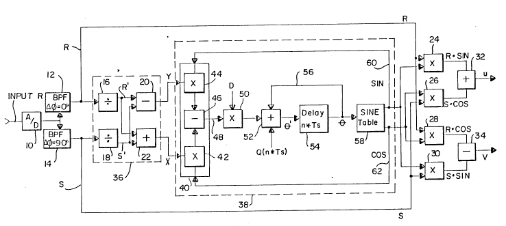
This background having been given, attention is
directed to Figure 3 wherein a digital embodiment of the
demodulator of the present invention is shown. Although
shown as discrete components in the embodiment of Fig.
3, it should be appreciated that each of these
components may also be interpreted or replaced in other-
embodiments by functions to be performed, for example, ~~-
as microcodes in a microprocessor.
As shown in Fig. 3, a phase modulated carriersignal R is input to a sampling means, such as an
analog-to-digital converter 10. The analog input
carrier signal is then converted by analog-to-digital
converter 10 into a multi-bit input carrier signal which
is transmitted to first and second bandpass filters 12
and 14. As is apparent, analog-to-digital converter 10
periodically samples input carrier signal R and produces
for each sample a multi-bit input carrier number
representing the amplitude value of the input carrier
signal R at the moment of sampling. Thus, there appears
at the output of analog-to-digital converter 10 a
continuous stream of multi-bit binary numbers, varying
in the same manner as the amplitude of the input phase
modulator carrier signal R. These discrete digital
number values represent the amplitude values at
periodically spaced points on the analog waveform.
These bits are fed to digital bandpass filters 12
and 14, which may be of the finite impulse response
(FIR) type. Filter 12 in essence filters out extraneous
noise and signals that are beyond its bandwidth so that
~ only the original transmitted signal (in the form of a
multi-bit signal) is output therefrom as R. The output
from filter 14, likewise, is the original transmitted
signal, but with a phase shift of 90. Implementing
filter 14 can be accomplished by means of well known
sine and cosine transformations for non-integrating
phase shifting of the output signal from filter 14
relative to that from filter 12. The output of filter
14 is represented as the signal S.
The respective signals R and S - are fed to
corresponding dividers 16 and 18 where~y the signals are
scaled, with the dividers acting as scalers for halving,
for example, the amplitudes of the respective signals.
The scaled signals R' and S' are input respectively to a
subtracter 20 and an adder 22. From there,
instantaneous estimates x and y of signal R' (the scaled
in-phase or cosine component) and signal S' (the scaled
quadrature-phase or sine component), respectively, of
the input carrier siqnal are provided. The expressions
for these carrier estimates are as follows:
x = Sin(w n Ts + P) = {R(n-Ts) + S(n Ts)}/2 (2)
y = Cos(w n l's + P) = {R(n-Ts) - S(n-Ts)}/2 (3)
where R and S are the real and imaginary
Fomponents, i.e. the in-phase and quadrature-phase
2000007
BC9-85-014
components, of the received signal; Ts is the sample period;
and P represents a phase offset between the actual carrier and
the sampling instant nTs.
Although referred to as the instantaneous estimates of the
cosine and sine components, it should be appreciated that
these estimates are only valid toward the centre of the baud
period, and are represented respectively by y and x in Figure
3.
In issued U.S. Patent # 4,849,706 the instantaneous
estimates x and y are sent directly to multipliers and adders,
such as multipliers 24 to 30 and adders 32 and 34.
For the present invention, however, the instantaneous
estimates of the in-phase and quadrature-phase of the input
carrier signal, output from subtracter 20 and adder 22, which
together with dividers 16 and 18, form an estimator circuit 36
enclosed by dotted lines, are fed to a differential carrier
recovery mechanism, designated 38.
Specifically, the instantaneous estimates x and y are fed
into a computational block 40 which has two multipliers 42 and
44, as well as a subtracter 46.
The x and y components, when they are input to
computational block 40, have information regarding only the
sine and cosine components of the input carrier signal. In
computational block 40, the x and y components are multiplied
and combined according to the following equation:
Sin(A-B) = Sin(A) - Cos (B) - Cos(A) Sin(B) (4)
where A represents the coherent carrier phase e and B
represents the phase implied in Equations 2 and 3.
It should be noted that the phase implied in Evaluations
2 and 3 is never calculated directly via
aOOO~
inverse sine and cosine functions since Equation 4 does
not require the actual sine and cosine angles. The
actual phase error, or phase angle deviation, can be
found by taking the sine of the phase error found in
S Equation 4, and performing an inverse sine function on
the value via a table lookup or other possible methods.
This process, however, can be avoided by noting that for
small angles, the sine of the angle is approximately
equal to the magnitude of the angle, in radian measure.
Therefore, as the recovered carrier approaches the
actual phase of the transmitted carrier, Equation 4
becomes a very good estimate of the actual phase error
of the carrier, and thus can be used for adjusting the
carrier phase to achieve a very accurate phase
synchronization. This phase error is output from
computational block 40, via line 48, and fed into a
multiplier 50, which acts as a scaler for multiplying
the phase error with a multiplication factor D.
The reason for requiring a multiplier 50 is that
when the phase error is first output from computational
block (for instance when the system is first initiated)
it tends to be very large. The invention employs a
convergence process so this large phase error can be
incrementally decreased, by means of feedback. While
Equation 4, at the beginning of its computation, is an
invalid expression of the actual phase error, the sign
of the output phase error does correspond to the sign of
the actual phase error. Hence, by continuously
converging the phase error (or phase angle deviation)
output from computational block 40, with some ideal
numbers, the phase error eventually will be corrected to
reflect the actual phase error.
To achieve this feedback, the scaled phase error is
sent next to a summer 52 which has as its inputs,
besides the scaled phase error signal (from summer 50),
a phase angle from an existing sample of the input
~oo~
ll ~
carrier signal and a phase shift proportional to the
differential phase shift between the baud period in
which the current sample of the input carrier signal was
taken and the baud period in which the existing sample
of the input carrier was taken. The phase shift is
represented by the expression Q(n Ts), which is
determined from the output of the demodulator,
represented by U and V, as shown in Fig. 2. In other
words, the expression Q(n-Ts) is the actual differential
phase shift detected by the demodulator and may be
obtained from a standard first order loop which tracks
the phase error as follows:
~ {(n+1) Ts} = ~ (n-Ts) - D E(n Ts) + Q(n-Ts) (5)
The actual differential phase shift Q(n-Ts) must be
added to the coherent carrier phase in order for the
instantaneous estimates X and Y to be in-phase with the
recovered carrier. This phase shift is also needed if
the demodulator is to generate differential phase shifts
directly. Alternately, a carrier signal may be
maintained without a phase shift being used in
demodulating absolute phase shifted signals, and the
running phase shift erm, Q, may be kept separately and
added to the carrier phase for calculation of the phase
error, and then taken away afterwards. In Equation 5,
E(n Ts) represents the phase error signal defined by the
following equation:
E(n-Ts) = sin(~) {~n-Ts) - S(n Ts)}/2 (6)
- sin(~) {R(n Ts) + S(n Ts~}/2
where Equation 5 was obtained by the substitution
of Equations 2 and 3 into Equation 4.
This is due to the fact that, during the initial
convergence, the coherent demodulation process cannot
provide a valid output phase shift, Q. Therefore, a
BC9-85-014 2 O0G007
"pseudo-coherent" demodulator such as that disclosed in
issued U.S. Patent #4,849,706, is used to provide initial
estimates of the phase shifts. After the initiation of the
phase convergence, the demodulator can be switched (by either
conventional firmware or software, not shown) to a coherent
mode in order to obtain better performance.
Continuing with Fig. 3, it can be seen that the phase
angle e' output from summer 52 is fed to a delay line 54,
which may be implemented as a memory. Delay line 54 insures
that the new phase angle e' output of summer 52 has in fact,
as part of its calculation, the existing angle e which was
provided as an output by delay Line 54 and fed back to summer
52, by means of feed back line 56. The separation of new phase
angle e' and phase angle e is by one baud period. Accordingly,
as new phase angles e are constantly being produced by summer
52, constantly updated phase angle e are fed back to summer
52, thereby effecting an averaging circuit for incrementally
decreasing the phase error signal from computational block 40.
The phase angle e is next fed to a sine table 58 which
may be a memory or a collection of memories. Although not
limited thereto, for this embodiment, phase angle e is assumed
to have an eight bit vàlue (since it is in a digital format),
and the eight bit value of e is used as an address for
selecting one of, for example, 256 possible entries (or
trigonometric functions) which had previously been stored in
sine table 58. Thus, in response to a new phase angle e, sine
table 58 provides a corresponding trigonometric function
comprising sine and cosine components to line 60 and 62,
respectively, to be fed back to computational block 40.
These sine and cosine components from sine table 58,
although being multi-bit numbers, actually do represent the
amplitudes of the sine wave and cosine
2000007
BC9-85-014
wave of the input carrier signal at the phase angle e which
has just been provided as an input to sine table 58. These
sine and cosine waveforms are coherent, although it must be
kept in mind that they only represent one sample of the sine
wave and one sample of the cosine wave for their particular
baud period; and it takes a plurality of these components to
fully represent the sine and cosine wave of the input carrier
signal.
The coherent sine and cosine components are next fed to
multipliers 24 to 30 and are combined in pairs by adders of 32
and 34 to provide O-ltpUt components U and V, as represented in
Fig. 2 and defined by the equations below.
U = Rosine + socose (6)
V = Rocose - Sosins (7)
With reference to Fig. 2, it can be seen that U and V
represent the amplitude values of the modulation components of
the input carrier signal R. For example, when U equals +1 and
V equals +1, a zero (0) degree phase shift is represented. If,
in the next baud period, a U of -1 and a V of +1 are obtained,
then it can be said that a phase shift of +90, corresponding
to an information dibit pair of (0,1) has been detected. The
dibit information, of course, relates to the actual data
information that is being conveyed by the analog input carrier
signal R, which is to be sent for additional processing, as
for example to a slicer whose output may be fed back to summer
block 52 as Q(noTs).
The discrete components of the Fig. 3 embodiment can be
replaced as functions and be performed by certain specialized
digital signal processing (DSP) microprocessors, such as that
shown in Fig. 4. In the embodiment of Fig. 4 a microprocessor
A 64 is connected
o~
,1
14
through a combination instruction data bus and address
bus 66 to a number of components. The phase modulated
input carrier signal R is fed to an analog-to-digital
converter such as 10 shown in Fig. 3. For the Fig. 4
embodiment, the steady stream of multi-bit binary
numbers are fed from analog- to-digital converter 10 to
data bus 66 and stored in sequential storage locàtions
of a random access read-write memory (RAM) 68. Also
includea in the Fig. 4 embodiment are a random-access
read only memory (ROM) 70 and an input/output interface
mechanism 72, which is connected by another data bus 74
to other input/output interface mechanisms.
Microprocessor 64, in addition to performing other
chores, controls the movement of the input carrier
multi-bit numbers ~rom analog-to-digital converter 10 to
RAM 68. A typical hardware multiplier (not shown) may
be added to this type of microprocessor to aid the
computation of the different previously discussed
e~uations. mhe microprocessor 64 executes various
program routines representing the different functions
performed by the components shown in the Fig. 3
embodiment.
These program routines are permanently stored in
ROM 70, which is also coupled to microprocessor 64. For
example, a first of these function program routines may
be analogous to the function performed by bandpass
filter 12. A second function program routine may
correspond to the function performed by estimator
circuit 36, i.e. the earlier discussed Equations 2 and
3. Similarly, a further function program routine may be
used for calculating Equation 4, also performed by
computational block 40 of the Fig. 3 embodiment. Of
course, it should be appreciated that these diff_rent
function program routines are performed in a microcode
format and the resulting coherPnt sine and cosine
components of the input carrier signal may still be
~o~o~
multiplied and added to form demodulator signal numbers
which represent the amplitude values of the input
carrier signal, as U and V.
Also, a memor~ may be partitioned in RAM 68 for
effecting the delay function of delay block 54, while a
portion of memory ROM 70 may be reserved for storing the
values representing the ideal sine and cosine components
stored in sine table 58 of the Fig. 3 embodiment. ~he
resulting demodulator signal numbers U and V are in turn
stored in RAM 68 and are to be used for further signal
processing operations such as slicing, decoding,
descrambling, and deserialization.
Referring to Fi~. 5, there is shown a plurality of
representative signal patterns at the different outputs
of the respective components shown in the Fig. 3
embodiment. The waveforms of Fig. 5 represent three
continuous baud periods. As is well known, a ~aud is a
unit of signaling speed and refers to the number of
times the state or condition of a signal line may change
per second. A baud period is the time interval in which
the state or condition of the signal is required to
remain the same.
As shown, the upper waveform in Fig. 5 represents
the input carrier signal at the output of bandpass
filter 12; while the second waveform represents the
phase shifted signal at the output of bandpass filter
14. As the cosine and sine components of the carrier
signal converge, with short term deviations due to
noise being eliminated as a result of the converging
process, waveforms representin~ the coherent sine and
cosine components of the carrier signal -- provided as
outputs from sine table 58 -- are output, as shown by
the middle two waveforms of Fig. 5. As illustrated, the
sine and cosine waveforms are shifted by 180 in baud
period BP 2, from baud period BP 1. Also, even though
there is no phase shift between baud period BP 2 and
~ooo~
16
baud period BP 3, there is still a change in the
patterns of sine and cosine waveforms for those baud
periods.
The last two waveform patterns are representative
S of the amplitude values of the modulation components of
the input carrier signal R and, as can be seen at the
center of the respective baud periods, U and V do
represent the ampli'ude values of the input carrier
signal. For example, for baud period BP 1, U has a +l
value while V has a -1 value, which correspond to a
dibit pair information of ~1,0). Likewise in baud
period BP 2, both U and V have -1 amplitudes. This
translates to a dibit pair information of (0,0). As for
baud period BP 3, both U and V have +l amplitudes
values, the dibit pair information contact becoming
(1,1) .
Although the phase change shown in Fig. 2 and
discussed so far relates to a change in the phase angle,
an absolute phase may also be used. For the absolute
phase scenario, instead of 0, 90, 180, and -90,
corresponding 45, 135, 225 and 315 are used. The
results remain the same.
An analog embodiment of the demodulator of the
present invention is shown in Fig. 6. For the Fig. 6
embodiment, carrier signal R is fed through a bandpass
filter 76 to a signal distribution line 78. A phase
shifter 80 phase shifts carrier signal R ninety degrees,
for generating ihe signal S. The R and S signals are
fed to modulators 82 to 88 and to respective attenuators
90 and 92 in an estimator circuit 94 (within the dotted
block). The carrier signals, after attenuation, are fed
to difference circuits 96 and 98. he outputs of the
different circuits are provided to the differential
carrier recovery circuit 100, more specifically to
modulators 102 and 104 of computational bloc~ 106 within
circuit 100. As in earlier embodiments, the input
200~007
BC9-85-014
signals are modulated by ideal analog signals, provided in
this embodiment by a voltage controlled oscillator 108, in
response to a predetermined phase angle e.
By means of a difference circuit 110, the modulated
signals from computational block 106 are provided as a phase
error signal (or a phase angle deviation) to an amplifier 112,
to be multiplied with a constant D. It should be appreciated
that D is a fractional constant for assuring that the
correction of the phase error signal is only performed in
incremental steps, instead of correcting for the entire error
in one single step, so that the signal will not become
unstable and oscillatory. The thus amplified signal is then
summed by a summer 114 with the predetermined phase-angle
provided by a sample and hold circuit 116 and a differential
phase shift, Q(noTs), which is proportional to the
differential phase shifts between the input carrier signal and
the predetermined input carrier signal.
By thus summing the original pre-existing phase angle e
and the current phase shift with the error signal, a new phase
angle e is calculated and transmitted to sample and hold
circuit 116, from whence a new phase angle e is calculated. As
before, this new phase angle e is fed back to summer 114 for
further calculations of new phase angles, and to voltage
controlled oscillator 108 for providing an input thereto so
that ideal cosine and sine waveforms can be output therefrom.
The ideal cosine and sine waveforms are fed back by feedback
lines 118 and 120, respectively, to computational block 106,
thereby effecting a feedback loop for averaging out the phase
error signal.
The thus produced sine and cosine waveforms are next fed,
in conjunction with carrier signals R and S, to modulators 82
to 88, paired and subtracted by the respective difference
circuits 122 and 124, for
~\
BC9-85-014 200qoo7
18
generating coherent demodulated signals U and V. The
demodulated signal U represents the in-phase baseband
component of the transmitted carrier signal, and for the
present invention, represents the binary value of the first
data bit in each transmitted dibit pair. The demodulated
signal V, on the other hand, represents the quadrature-phase
baseband component of the transmitted carrier signal, and is
representative of the binary value of the second bit in the
transmitted dibit pair. Both waveforms of the demodulated
signals U and V are similar to that shown for the U and V
waveform patterns in Fig. 5. And as can be readily seen from
Fig. 6, the demodulated signals U and V have the same
respective expression as equations (6) and (7). By proper
substitution, these equations, as was done in issued U.S.
Patent #4,849,706, are representative of the peak amplitude
values of the sinusoidal components of the input carrier
signal.
Inasmuch as the present invention is subject to many
variations, modifications, and changes in detail, it is
intended that matter described throughout this Specification
and shown in the accompanying drawings be interpreted as
illustrative only and not in a limiting sense. Accordingly, it
is intended that the invention be limited by the spirit and
scope of the appended Claims.
,~