Note: Descriptions are shown in the official language in which they were submitted.
~QC)Q324
MILLIMElE~ I~AVE MICROSTRIP MODULATOR/SWITC}I
BACKGROUND OF THE INVENTION
: Field of the Invention
This invention relates to microstrip Ll csion lines and
microstrip transmission line c~r, ~~ts operating in the 11 -ter wave
region of the frequency spectrum and more particularly to a microstrip
~ tor/switch for use with such microstrip transmission lines and
microstFipc, ~r-~ts.
. .
.
.
' ' - ' ' ' ' . ' , ' ' '
", ' ' ,~ ~ . ' ~
2~0(~324
Description of the Prior Art
~ odulator/switch devices suitable for use with microstrip
transmission lines and microstrip components operating in the millimeter
wave region of the frequency spectrum have not heretofore been developed.
Since much equipment has been developed today for use in the mill; ter
wave region of the frequency spectrum and since such equipment is often
designed with planar circuitry utilizing microstrip transmission lines
and microstrip c~mr~nPnts because of the substantial savings in size and
weight achieved thereby, a need has arisen for a microstrip modulator/
switch which is capable of operating in this region of the frequency
spectrum. For example, such microstrip modulator/switch devices could
be used to ~ dulate m;ll; -ter wave energy for various systems applications
or could be used as a protective type switch in radar systems and the
like to protect sensitive millimeter wave receivers during the time that
the mill; ~er wave transmitter is transmitting.
Essentially, a modulator/switch device suitable for use in the
millimeter wave frequency legion must provide a useful change in insertion
loss for the device when the device is actuated. The device should have
a first transmission sta~e in which it provides a low attenuation of
the applied RF electromagnetic wave signal and consequently exhibits a
low device insertion loss and a second tr~n~ csion state in which it
~: ~
~ - 2 -
ZQO(~324
provides a high attenuation of the applied RF signal and exhibits a high
device insertion loss. The device must also be capable of being switched
from one of the foregoing states to the other with only a mini~m amount
of switching energy. For exampleJ when the device is used as the
a~o~ ioned protective switch for radar applications and the like,
the device would be placed in the high loss state during the time that
the radar transmitter is transmitting to protect the receiver of the
radar set from the transmitted pulse and then actuated to the low loss
state when the transmitter is not operating.
A suitable microstrip ~ dulator/switch for use in the rill; ter
wave frequency region should also have a -~h~nic~lly-rugged construction
which is light in weight, compact in size and which is relatively
inexpensive to manufacture and maintain. Because devices exhibiting
the aforementioned useful change in insertion loss or attenuation
characteristics are often called upon to act not only as switches but
also as modulators, the term "microstrip switch" as used hereinafter in
the specif;c~tion and claims of this application shall be deemed to
mean a device which is capable of functioning both as a modulator and a
switch.
SU~UURY OF THE INVENTION
It is an object of this invention to provide a microstrip switch
_ 3
.:
' ' - ,
. . . . . .
: . . : .. . . .
. . : . . .
.
2QOQ324
which is suitable for use in the millimeter wave r,egion of the frequency
spectrum.
It is a further object of this invention to provide a microstrip
switch which is capable of being switched from one transmission state to
the other tr~n~m;csion state with a ;n;~ amount of switching energy.
It is a still further object of this invention to provide a
microstrip switch of merh~n;~l1y-rugged construction which is compact
in size and low in weight and which can be lf~ctured and maintained
relatively easily and inexpensively.
It is another object of this invention to provide a microstrip
switch which is especially suitable for use in '11; -ter wave radar
systems and the like.
Briefly, the microstrip switch of the invention comprises a
length of microstrip transmission line dielectric substrate having top
and bottom planar surfaces and an electrically conductive ground plane
mounted on the bottom surface of the substrate. A ferrite rod having a
rectangular cross-section and a dielectric constant greater than the
dielect,ric constant of the substrate is mounted on the top surface of
the substrate with one of the four sides of the rod abutting the sub-
strate top surface and with the ends of the rod spaced a distance from
the ends of the length of substrate. A pair of ramp-shaped dielectric
waveguide members is mounted on the top surface of the substrate at the
ends of the rod. Each of the r$mp-shaped members has a dielectric
- 4 -
...
... ~ -- - .
'. -: ., , - -, :
- . .- .-.:. :
.
:
2QOQ32~
con.stant which is substantially the same as the dielectric constant of
the rod, a width which is substantially the same as the width of the
rod, a planar bottom surface abutting the top surface of the substrate,
an end surface abutting the end of the rod adjacent thereto ana a down-
wardly-sloping planar top surface extending between the end of the rod
adjacent thereto and the top surface of the substrate. A first length
of electrically conductive microstrip conductor is mounted on the top
.. surface of one of the ramp-shaped members and the top surface of the
substrate in ~ rment with the longitudinal axis of the rod and extending
between the end of the rod adjacent the one ramp-shaped member and the
end of the length of substrate adjacent the one ramp-shaped member. A
second length of electrically conductive microstrip conductor is mounted
on the top surface of the other of the ramp-shaped members in alignment
with the longitudinal axis of the rod and extending between the end of ..
the rod adjacent the other ramp-shaped member and the end of the length
of substrate adjacent the other ramp-shaped member. Finally, selectively
operable means are provided for applying a unidirectional magnetic
field along the longitudinal axis of the rod to cause Faraday rotation
of elec~ netic wave energy traveling through the rod, whereby the
ends of the first and second lengths of microstrip conductor adjacent
the ends of the length of substrate act as the terminals of the microstrip
switch and the ferrite rod controls the passage of ele~ gn~tic wave
.
:: 5
."''' ' , ' ...
.
.. , ~ , .
~ '
- . , .
,
.. . .
2noo324
energy between the terminals of the switch.
The nature of the invention and other objects and additional
advantages thereof will be more readily understood by those skilled in
the art after consideration of the following detailed description taken
in conjunction with the ~cc~ , ying drawings.
BRIEF DESCRIPTION OF THE DRAWINGS
In the drawings:
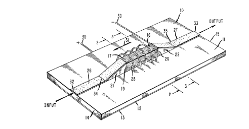
Fig. 1 is a peTspective view of the microstrip switch of the
invention;
Fig. 2 is a full sectional view of the microstrip switch taken
along the line 2-2 of Fig. l;
Fig. 3 is a full sectional view of the microstrip switch taken
along the line 3-3 of Fig. l; and
Fig. 4 is a perspective view of one of the ramp-shaped dielectric
~ waveguide members shown in Fig. 1.
;
DESCRIPTION OF THE PR~FERRED EMBODDMENT OF THE INVENTION
Referring now to Figs. 1-3 of the drawings, there is shown a
- 6 -
.
.
:
.
. , . . . '. ~ .
- : ' :
2C~0~324
microstrip switch constructed in accordance with the te~hings of the
present invention comprising a length of microstrip transmission line
dielectric substrate, indicated generally as 10, having a planar top
surface 11, a planar bottom surface 12 upon which is mounted an
electrically conductive ground plane 13 and ends 14 and 15. The substrate
10 may, for example, comprise a section of conventional microstrip
tr~n ~~sion line subs~rate which is approximately 0.010 inch thick
and which is fabricated of duroid or other similar dielectric material
having a relatively low dielectric constant. The electrically con-
ductive ground plane 13 covers the entire bottom surface 12 of the
substrate and should be fabricated of a good electrically conductive
metal, such as copper or silver, for example.
; A ferrite rod, indicated generally as 16, having a rectangular
cross-section, a top side or surface 17, a bottom side or surface 18
and ends 19 and 20 is mounted on the top surface 11 of the substrate
with the bottom side 18 of the rod abutting the substrate top surface
; and with the ends 19 and 20 of the rod spaced a distance from the
correspon~;ng ends 14 and 15, respectively, of the substrate length 10.
~le rod 16 is fabricated of a ferrite material, such as nickel
zinc ferrite or lithium zinc ferrite, for example, which exhibits
netic behavior in the presence of a unidirectional sa5netic field.
- 7 -
. . .
~ .
... .
200~324
The dielectric constant of the ferTite rod 16 is greater than the
dielectric constant of the substrate 1~. For example, if the substrate
is fabricated of duroid, it would have a dielectric constant of 2.2
and if the ferrite rod is fabricated of nickel zinc ferrite, the rod
would have a dielectric constant of 13.
As seen in Fig. 1 of the drawings, a pair of ramp-shaped
dielectric waveguide members, indicated generally as 21 and 22, is
mounted on the top surface 11 of the substrate 10 at the ends 19 and 20
of the ferrite rod 16. Each of the ramp-shaped members 21 and 22 has
a dielectric constant which is substantially the same as the dielectric
constant of the rod, a width which is substantially the same as the
width of the rod 16, a planar bottom surface abutting the top surface 11
of the substrate, an end surface abutting the end of the rod adjacent
thereto and a downwardly-sloping planar top surface extending between
the end of the rod adjacent thereto and the top surface of the substrate.
For example, the ramp-shaped dielectric waveguide member 22 which is
shown in Figs. 1, 3 and 4 of the drawings is seen to have a width W
which is substantially the same as the width of the rod 16, a downwardly-
sloping planar top surface 23 which extends between the end 20 of the
rod 16 adjacent thereto and the top surface 11 of the substrate, a
planar bottom surface 24 which ~buts the top surface 11 of the substrate
. - 8 -
..
2C!0Q3Z4
ancL an end surface 25 which abuts the end 20 of the rod which is adjacent
thereto. The ramp-shaped member 21 is of identical construction to the
ramp-shaped member 22 except that its end surface abuts end 19 of the
ferrite rod 16. Both of the ramp-shaped members 21 and 22 should be
fabricated of a material having a dielectric eonstant which is sub-
stantially the same as the dielectric constant of the ferrite Tod 16.
For example, if the ferrite rod is fabricated of nickel zinc ferri~e,
the ramp-shaped members 21 and 22 may be conveniently fabricated of
magnesium titanate which also has a dielectric constant of 13. In order
to min- ~7e the insertion loss of the microstrip switch when the switch
is in the low loss transmission state, the ends 19 and 20 of the ferrite
rod 16 may be joined to the corresponding end surfaces of the ramp-
shaped members 21 and 22 by means of a low loss epoxy or adhesive, such
as Scotch-Weld Structural Adhesive, for example, which is marketed by
the 3M Company of St. Paul, Minn.
As seen in Fig. 1, a first length of electrically conductive
microstrip conductor 26 is mounted on the downwardly-sloping top
surface of the ramp-shaped member 21 and the top surface 11 of the sub-
strate 10. The microstrip conductor length 26 is aligned with the
longitudinal axis of the rod 16 and extends between the end 19 of the
rod which is adjacent the member 21 and the end 14 of the length of
:
200Q324
substrate which is also adjacent the member 21. The longitudinal axis
of the rod although not illustrated would correspond to the line formed
by the directional arrows labeled "Input" and "Output" in Fig. 1. In a
similar f~shion~ a second length of electrically conductive microstrip
conductor 27 is mounted on the top surface 23 of the other ramp-shaped
member 22 in alignment with the longitudinal axis of the rod and
extends between the end 20 of the rod adjacent the member 22 and the end
15 of the substrate length 10 which is adjacent the member 22. The micro-
strip conductor lengths 26 and 27 should be fabricated of a good
electrical conductor, such as copper or silver, for example.
The microstrip switch of the invention also has selectively
operable means for applying a unidirectional magnetic field along the
longitudinal axis of the rod 16 to cause Faraday rotation of electro-
magnetic wave energy traveling through the Tod. As shown in Figs. 1 and
2 of the drawings, the afo~ tioned means m~y take the forn of a
h~l;c~l coil 28 which encircles the rod 16 and extends along the length
of the rod. As seen in Fig. 2, the turns of the coil 28 are embedded
in and pass through the substrate 10 and also pass through small
apertures 29 in the ground plane 13. The turns of the coil 28 should be
spaced a distance from the ferrite rod 16, ~s illustrated, for proper
operation of the microstrip switch. The wire from which the coil is
fabricated should be insulated to pre~rent sections of the coil from being
2~!0C132~ -
shorted out by the ground plane 13. When the terminals 30 of the coil
are connected to a source of d.c. voltage, a unidirectional magnetic
field represented by the arrow 31 in Fig. 1 will be formed which extends
the length of the ferrite rod 16 along the longitudinal axis of the rod.
The magnitude and direction of the magnetic field 31 may be controlled
by the amplitude and polarity, respectively, of the d.c. voltage applied
to the coil terminals. For the voltage polarity illustrated in Fig. 1,
$he magnetic field would have the direction shown by the arrow 31.
The terminals of the microstrip switch are formed by the ends 32
and 33 of the first and second lengths 26 and 27, respectively, of
microstrip conductor as shown in Fig. 1. In operation, when a 11; -ter
wavelength signal is applied to the Input terminal 32 of the switch, it
is transmitted along that portion of microstrip conductor length 26
which is mounted on the top surface 11 of the substrate 10 because that
portion of the microstrip conductor 26 in conjunction with the ground
plane 13 and the dielectric substrate 10 form a short section of a
; conventional microstrip transmission line. When the applied signal
reaches the bottom (shown by the line 3~) of the ramp-shaped dielectric
waveguide member 21 itthen passes along a microstrip transmission line
which is formed by the portion of microstrip conductor length 26 which
is on the upwardly-sloping top surface of the ramp-shaped member 21 and
- 11 -
21~0Q324
the ground plane 13 and the dielectric substrate lO. However, as the
signal is progressing up the incline it begins to become transmitted
by the solid dielectric waveguide material of the ramp-shaped member 21
because the dielectric constant of the ramp-shaped member 21 is sub-
stantially greater that the dielectric constant of the substrate lO.
When the applied signal Teaches the top of the upwardly-sloping
top surface of the ramp-shaped member 21 it becomes completely captured
by the ferrite rod 16 which acts as a solid dielectric waveguide having
the same or substantially the same dielectric constant as tlie ramp-
shaped member 21. If the coil 28 is not energized, the applied RF
signal is transmitted by the ferrite rod in the dielectric waveguide
mode of transmission with very little loss to the ramp-shaped dielectric
waveguide member 22 which has a portion of the microstrip conductor
length 27 mounted on its downwardly-sloping top surface 23. Here, the
reveTse process ta~es place and the ~ignal becomes gradually recaptured
by the microstrip transmission line mode of transmission. By the time
the applied signal reaches the Output terminal 33 of the switch, it
will have been completely recaptured by the microstrip transmission line
mode of operation.
If the coil 28 is energized by a suitably applied d.c. voltage,
the unidirectional magnetic field 31 which is produced along the
!
- 12 -
Z~0~324
longitudinal axis of the ~errite rod 16 will cause the ferrite rod to
rotate the applied signal passing through the rod approximately 90
degrees because of the well-known Faraday rotation effect which is
produced by the interaction of the magnetic field and the g~ n~tic
properties of the ferrite. Since the applied RF signal is now rotated
approximately 90 degrees, the applied signal will no longer be properly
oriented for transmission along a microstrip transmission line and a
scattering of the signal will be produced. The scattering of the
signal resulting from the misalignment of the signal with the microstrip
trAn csion line results in a high applied signal loss. Accordingly,
very little of the applied RF signal will reach the Output te, 'n~l 33 of
the switch. By selectively energizing the te n~ls 30 of the coil 28,
the microstrip switch may be placed in either its high loss tr~n ssion
or off state or its low loss transmission or on state. It will be noted
that the microstrip switch of the invention is bidirectional in operation
so that the applied RF ele~tr~ ~gnetic wave energy signal m~y be applied
to either terminal 33 or tel n~l 32. Additionally, it should be noted
that the direction of the magnetic field 31 will not affect the operation
of the switch so that a reversal of polarity o~ the d.c. control signal
applied to the c~ntrol tel n~ls 30 of the switch will not affect ths
bidirectional operation of the switch. Although the aLor~ tioned
description of switch operation and construction has been gi~en with
- 13 -
XQO(~32~
reference to an applied signal in the millimeter wave region of the
frequency spectrum, it is apparent that the use of the switch is not
limited to signals in this region of the frequency spectrum. Pre-
liminary testing of a microstrip switch constructed in accordance with
the invention using a ferrite rod approximately 0.6 inch long and
operating in the 35 G}~ region of the frequency spectrum indicates that
the switch should provide greater than 15 dB loss for the high attenuation
or off state and a 1 dB insertion loss for the low attenuation OT on
state.
It is believed apparent that many changes could be made in the
construction and described uses of the foregoing microstrip switch and
many seemingly diffe~ t embodiments of the invention could be con-
structed without departing from the scope theTeof. FOT example, each of
the lengths 26 and 27 of microstrip conductor could be fabricated in
two separate sections which are elec~rically interconnected by means
such as soldering. The two sections of conductor length 26 could be
electrically interconnected along the line 34 at the bottom of the sloping
top surface of ramp-shaped member 21 and the two sections of conductor
27 could be interconnected at the line 35 at the bottom of the ramp-
shaped member 22 as shown in Fig. 1. Accordingly, it is intended that all
matter contained in the above description OT shown in the PeC .~nying
drawings shall be interpTeted as illustrative and not in a limiting sense.
- 14 -
'" :' '-- ' ' :