Note: Descriptions are shown in the official language in which they were submitted.
38
; LEAD FRAME FOR A MULTIPLICITY OF TERMINALS
Backqround of the Invention
Field of the Invention
The present invention relates to a lead frame
for a multiplicity of terminals, in particular of
large-scale integrated semiconductor chips, arranged
in a very confined space and consisting of metallic
~ .,
conductors, which converge from large outer spacings
toward the terminals and can be connected to the
terminals.
Discussion of Related Art
Such lead frames are used for contacting one
` or more large-scale integrated semiconductor chips.
On their outer edge, the semiconductor chips have
bonding pads which, according to the current
technique, are square and have an edge length of
~y go~m - 120~m and a spacing from pad to pad of at
~j least 30~m. The contact to the inner ends of the
'~l conductors of the lead frames is usually established
by bonding wires having a diameter of 25~m - 30~m.
The lead frames are usually produced with
` outer edge pieces which are parted or separated
,
~' . ' '
,,' j~
',`;;.
., ~ ' .
., .
., .
~3Q~8
after positioning of the lead frame, so that the
individual conductors of the lead frame are no
longer electrically connected to one another.
Punching is the least expensive method
available for the production of the lead frames.
Due to the relatively high tool costs, this
production method is not flexible. For relatively
high numbers of terminals, the complexity of the
tools increases, with the result that problems of
precision multiply. Therefore, this technique is
used to realize terminal numbers up to about 120.
Another known method of producing these
frames is etching, by which the desired structures
- are etched out of a uniform metallic surface, so
that the desired metallic conductors remain. The
etching operation can be controlled in the usual way
by photographic shadowing methods. Although this
method is distinguished by low tool costs and by
high flexibility, it leads to relatively high
; 20 production costs because automation has not yet
succeeded on an economically significant scale.
Both methods lead to a minimal terminal width
~ and to a minimal clearance spacing between the
; terminals of the conductors on an order of magnitude
of the material thickness, which is, for example,
` 150~m. The minimal terminal width of 150~m and the
minimal spacing of likewise 150~ leads to a
terminal grid of 300~m. On account of the limited
length of the bonding wires, according to known
~ 30 techniques, a number of terminals of up to 160 can
`~ be achieved with a square package of 28mm edge
~ ''
,
.
, . .
^.' :
- - , . ~ - . .. . .
.: - . -, .
Z~338
..
length (EIAJ Standard). Higher numbers of terminals
can be achieved only by expensive special package
configurations. These special packages, so-called
` arrays, have the disadvantage however that they are
not suited for modern non-thruplating insertion and
soldering methods.
One known method of producing very small
terminal groups is based on the use of a tape
carrier material (e.g. polyimide), on which a
terminal grid is produced by the positive or
negative method and in assembly is connected
directly to the chip by soldering. The amount of
solder necessary for this is applied in a number of
additional processes, starting from the chip. With
this "tape automated bonding", terminal widths of
50~m with a spacing of 30~m, that is a grid pattern
~, of 80~m, can be realized. However, this method is
relatively expensive and inflexible. High tape
material and tool costs arise, which have to be
funded anew with every change in chip design.
Therefore, a cost-effective production of relatively
small numbers is not possible. Furthermore, these
~, products require special insertion techniques at the
` customer's premises.
., .-
Summary of the Invention
One object of the invention is to provide a
lead frame of the type mentioned above which is
-: inexpensive to produce and allows for a high number
of terminals.
:~ .
. ~ .
_3_ ~
:: .
.,~' ~".
:, '
.', :
.. . . ... . . .
. .. - . . ., - .,. : . . : . , :., ,: ., , . :
38
According to the invention, this object is
achieved by the metallic conductors being produced
in an outer region by a conventional production
method and at their ends pointing toward the
terminals by laser cutting of uniform metallic
. .
material.
According to the invention, for the first
time a combination of more than one production
method is undertaken for producing the conductors of
the lead frame. The invention is based on the
realization that the conventional methods are
adequate for the larger spacings in the outer region
-~ of the lead frames, meaning that the most favorable,
usually the least expensive, method is selected for
each application. The limitation of the
interconnection density is due to the disadvantages
~ of the conventional methods, which do not allow a
`~ reduction in the spacing between the terminal ends
- of the conductors. According to the invention, a
laser cutting method is employed at the inner end of
;~ the conductor track, so that once the conventional
method has been applied to the outer ends of the
conductors a uniform metallic surface remains on the
inside, which can then be divided by laser cutting
into the desired extensions of the conductors
produced. Laser cutting is very flexible, but
requires a relatively great deal of time. However,
the time required is not critical for the production
~r of the lead frame according to the invention,
because only the small sections at the inner end of
the conductors are produced by laser cutting, while
.:'
-4-
.', ~
, :
.
.' ~ '.
- 2a~ 38
. .
ordinarily the greater length of the conductors is
produced by the conventional quick methods, such as
punching or etching.
Brief Description of the Drawings
The invention is explained in more detail
below with reference to the enclosed drawing, in
which:
Figure 1 is a plan view showing conductors of
a lead frame according to the invention, which
conductors terminate adjacent a bonding pad, and
Figure 2 is a plan view showing the
conductors according to Figure 1 connected by
bonding wires to terminal areas of a semiconductor
chip.
~` '',
Detailed Description of the Preferred Embodiments
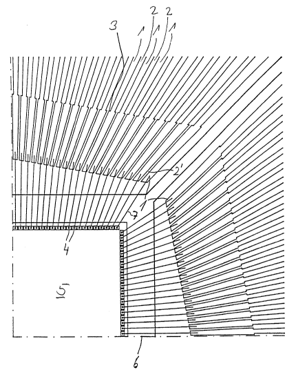
^ Figure 1 illustrates a multiplicity of
approximately star-shaped conductors 1, which are
~; relatively wide in the outer region of the lead
frame and are separated from one another by likewise
- 20 relatively wide intermediate spaces 2. Contacts cani~ be attached to the conductors 1 at their outer ends
by conventional techniques.
;~ The conductors 1 are produced over a large
- part of their length by a conventional technique,
for example by etching or punching. Where the
` converging profile of the conductors 1 causes the
width of the conductor track to reach a lower
..
,
.':! ,
"; ;,. '
'
.'~ , ,,
, ' ' :
!, ; ~
3~38
acceptable limit on the basis of minimal spacing 2
to be maintained, there is formed in the conductor
track 1 a step 3, by which the conductor tracks are
widened again and are separated by a very narrow
spacing 2' of constant width. The spacings 2' of
constant width are produced by laser cutting the
originally uniformly formed metallic material within
the step 3. Laser cutting allows very small widths
of the spacings 2' to be realized, so that the grid
spacing of the conductors 1 at the inner end of the
lead frame corresponds approximately to the grid
dimension of bonding pads 4 of a semiconductor chip
5 or is only slightly larger.
Figure 2 shows a semiconductor chip 5, which
is positioned on a bonding pad 6 within the lead
; frame. The connection of the individual bonding
;~ pads 4 to the metallic conductors 1 is made by usual
; bonding wires 7.
On account of the small grid spacing arising
at the inner end of the conductors due to the small
width of the spacings 2', the conductors 1 can be
` led very closely up to the bonding pad 6, so that a
high terminal assignment can be realized with short
bonding wires.
, . . .
,,; .
''"` ' ':
; ~ -.
.' "
~; '-'
'''' '''
,. .
. . .
.,' , .
, - ., . .: :. , . ~ . . : ,. . .