Note: Descriptions are shown in the official language in which they were submitted.
_, 2~JoG~7~
Field of the Inventlon
A systern for performing a serializlng control of a
reference to a maln storage.
Brief Description of the Drawinqs
Flgures lA, lB and lC show structural vlews of
the lnformation processing apparatus in whlch the CPU commonly
owns the maln stora~e apparatus,
Figure 2 shows a prior art timing chart of the
pre-serialized control,
Flgure 3 shows a prior art timing chart of the
post-serlallzed control,
Flqure 4 shows the prlnclple structure of the
present lnvention,
Figure 5 shows an explanatory drawing of the
seriallzatlon control operation according to the present
lnvention,
Figure 6 shows the structure of the system control
interface accordinq to an embodiment of the present inventlon,
Figure 7 shows the detalled structure of the
serlalizatlon notiflcation control signal circuit of the
embodiment in Figure 6,
Figure 8 shows a detailed circuit of a distribution
circuit of Figure 6,
Flgure 9 ls a timing chart of an embodlment of the
pre-serialized control,
Figure 10 is a timing chart of an embodiment of the
post-serialized control,
~.
~ 28151-1
200G'~35
Flgure 11 shows a timing relatlonshlp of serlali-
zatlon notlflcatlon slgnals produced by CPU-0, - 1, and -2
Figure 12 is a tlming chart of the embodlment in
whlch the lnterlock by the serialization according to the
present invention is overlapped with the other interlocks.
Backqround of the Invention
The present lnventlon relates to a system for
performlng a serlallzlng control of main storage references
between CPUs ln an lnformatlon processlng apparatus ln whlch
the main memory storage is commonly owned by a plurality of
CPUs .
A plurality of fetch or store accesses from a CPU to
a maln storage apparatus are generally conducted ln parallel.
It is necessary to ensure that these accesses are conducted ln
accordance wlth a predetermined order of instructions and that
an lnstruction is executed ln accordance wlth a predetermined
set of operands ln a predetermlned order.
In partlcular, if a cache memory is employed, a
STORE ls conducted through a maln storage and ls thus slow,
but a FETCH ls conducted only through a cache and ls thus
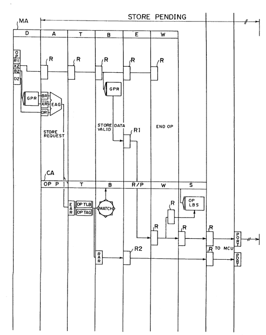
fast, as shown ln Flgures lA and lB. As shown in Flgure lA,
an lnstructlon I comprlses an OP code and address portions R1,
X2, B2 and D2. A STORE ls conducted as follows. In a
p~pellne operatton MA for a main storage access, an OP code of
an lnstructlon I ls decoded ln a D-cycle and the lnstruction I
is used for accessing a general purpose reglster GPR. Slgnals
of the address portlon are transmltted through reglsters R.
28151-1
"
2000435
-
In an A-cycle, the contents of GPR are added to a dlsplacement
D2 of the address portion for a loglc address at adder EAG,
thereby provlding an effective address. Then, in a pipellne
operation CA for a cache access, the prlorlty for a store
request ls determlned in an OPP cycle. In a T-cycle, it is
detected whether or not the effectlve address exlsts ln a
cache LBS. If the effectlve address matches the address
exlstlng ln the cache, a real address for accesslng the cache
LBS ls set in real address register RAR. On the other hand,
ln a B-cycle, the WRITE data is obtalned from general purpose
register GPR based on the address transmitted from lnstruction
I. In an E-cycle, the WRITE data and the real address are
respectively set ln reglsters Rl and R2. The WRITE data are
stored ln reglsters R and R ln a W-cycle and ln cache LBS ln
an S-cycle. Write data and address are respectlvely
transmltted to the MCU through reglsters R and ports PORT to
store the WRITE data in the main storage after a completion of
one execution cycle of one lnstruction. Therefore, lt takes
time to store the WRITE data in the main storage.
A FETCH operatlon ls shown ln Flgure lB. In an
A-cycle, the effective address is obtained based on the
address portlon of lnstructlon I and lt ls determlned in a
T-cycle by referring to TAG, whether or not the address exists
ln cache L~S . If lt does, the data ls obtalned f rom cache LBS
in a B-cycle and transmltted to register OWR ln an E-cycle.
It ls thereby sub~ected to a fetch operatlon before a
completion of an executlon cycle of an instructlon.
28151-1
", .
20~043~
.
Therefore, when a FETCH lnstruction ls produced
after a STORE lnstructlon, the actual fetch operatlon ls
completed before the STORE operatlon. Thus, prevlous data on
which the result of STORE is not yet reflected, ls fetched by
the FETCH operation. In order to fetch the new data on which
the result of STORE ls reflected, lt ls necessary to perform a
serlallzing process by provldlng a seriallzatlon request
slgnal.
In some informatlon processing apparatuses a common
memory apparatus ls owned by a plurallty of CPUs. In these
apparatuses a case arlses in which a plurallty of stores must
be conducted by a CPU and be observed ln accordance wlth an
execution order from the CPUs when respective CPUs perform
processes uslng a common area ln the maln memory apparatus.
In this case, when a certain process of several
lnstructions or an interruptlon is conducted, a particular CPU
must observe that another CPU completes lts store access to
the maln CPU and then obtalns a fetch access to a subsequent
maln storage apparatus. The process for ensurlng that this
sequence ls followed ls called seriallzatlon.
The serlallzlng process ls conducted as follows
1. A flrst operatlon ls conducted durlng the perlod from
when a partlcular CPU transmits the serlalizatlon request
after a store pendlng signal become~ 0 to when the MCU
recelves the seriallzation completlon slgnal. Thls is the
perlod durlng whlch the followlng fetch operatlon ls stopped.
2. A second operation ls conducted durlng the perlod
28151-1
,~
2000435
from when the MCU receives the serlalization request to when
it completes dlstrlbutlng lt to CPUs other than the partlcular
CPU .
3. A thlrd operatlon ls conducted durlng the perlod from
when the request for an lnvalldatlon of a cache is completed
by a store prevlously executed by the CPU after the other CPUs
receive the serlalizatlon request. Thls ls the perlod durlng
which the process of maklng access to the maln storage ls
stopped.
The CPUs' parallel processlng ability should be
increased so that the serializlng process ln a main storage
access ln a plurality of CPUs is executed at high speed.
Figure lC shows a structure of an information
processing apparatus of a type to which the present lnvention
ls directed.
In Figure lC, lN+lCPUs 1-0, 1-1... and l-N (N is an
integer larger than 1) operate ln parallel. Maln control
apparatus (MCU) 2 deals with an access request of respectlve
CPUs and maln storage unlt (MSU) 3 ls commonly owned by
respective CPUs. Caches 4-0 to 4-N, comprislng a hlgh-speed
small-capaclty buffer, are provlded at respectlve CPUs and
constltute a layer memory apparatus together wlth a maln
storage unit MSU. Instructlon control portlons 5-0 to 5-N are
provtded for respectlve CPUs and perform an executlon
lnstructlon control using a pipellne.
A store-in and store-through functlon exists for
controlllng these caches. Store-ln means that STORE ls
28151-1
- 2~0:043~
reflected only on a cache upon an executlon of a store, and a
group of data to be stored ls reflected on maln storage unlt
MSU when the serlallzation ls conducted or when the STORE of
the particular CPU ls reflected ln all the other CPUs.
Store-through ls a method for always reflectlng the STORE to
the maln storage unlt MSU every tlme STORE ls performed.
The serlallzatlon process differs greatly dependlng
on whether the cache control method ls a store-ln or a
store-through. Examples of both cases are descrlbed as
follows.
For a store-ln, the store ln whlch the control ls
classlfled depends on whether the area ls prlvate or publlc.
In a publlc area, the contents of the cache are reflected ln
the maln storage unlt MSU upon serlallzatlon. When the
cachlng operatlon ls invalldated, the next access to the main
storage is performed so that the most recent data ls obtalned
from the maln memory unlt, thereby ensuring that the
serlallzatlon operatlon ls executed.
For a store-through, the stores of respectlve CPUs
are generally reflected ln the maln storage unlt MSU and, when
the data of the store area ls malntalned in caches of other
CPU, the data ln the other CPU are lnvalidated. Thus, a
reflection process is executed. For a CPU whlch performs the
~erlalization, the followlng access to a maln CPU ls ~elaye~
untll the process of reflection to other CPUs ls completed.
Two serlallzlng methods are avallable, based on the time
relatlonshlp between a maln memory access of the operatlon
-- 6
28151-1
. ~
2900435
-
unit accompanled by the serialization and a main memory access
of the seriallzation sub~ect.
The first ls a pre-serializing method. This method
ensures that an access to a main memory in an operation unit
which is conducted after an access to a main memory preceding
an access to the operation unit accompanied by serialization
is completed. The other ls a post-serializing method. Thls
method ensures that the main access which follows the
operation unit accompanied by the seriallzation after the
operation unit is completed.
Figure 2 shows a timing chart of an operation
according to a prior art control using a pre-serializing
operation. Figure 10 shows a timing chart of the prior art
control for a post-serializing operation. The prior art
pre-serializlng shown in Figure 2, is explained as follows.
1~ shows an execution flow in a pipeline operation of the
instruction accompanied by a serialization. D shows an
instruction decode, A shows arithmetic of the effective
address for the operand, T shows an address translation
conducted by accessing a TLB and a detectlon of the exlstence
of data in the buffer by accessing a TAG. B shows a
buffer(cache) access, E shows an execution, and W shows a
writing of the result. LBS shows cache, EAR represents the
effec~ l~e address reglster, and OWR shows an operand word
register.
2) is a store pending signal transmitted to a CPU when
the memory control unit the MCU is processing the storing
, 28151-1
~000435
~ ,
request precedlng the lnstructlon to be serlalized. The store
pendlng signal is on untll a STORE operatlon ls entered lnto a
plpe-llne operation of the MCU after an A-cycle starts, as
shown ln Flgures lA and 2.
3) is a serlalization request signal, transmltted after a
store-pendlng slgnal ls turned off, for the CPU performlng a
serlalizatlon to conduct a serlallzation request.
4) ls a perlod of serlallzatlon processlng ln whlch the
MCU lnforms the other CPU of a serlallzatlon request, and the
result of the store precedlng the CPU ls reflected ln the
cache by another CPU (l.e. the cache ls invalldated) for thls
perlod. The other CPU stops the access to the maln CPU.
5) shows a serlallzatlon completlng slgnal transmltted to
the CPU whlch performs the serlallzatlon after the
serlallzatlon process 4) is completed. The CPU completes the
seriallzatlon process when lt recelves thls slgnal.
6) ls an lnterlock perlod, ln whlch the executlon ln the
lnstructlon executlon of 1) ls delayed by the serlallzlng
operation. The fetch operation of the operand uslng the
address generated durlng the A-cycle ls kept waltlng for thls
lnterlock, and ls carrled out through LSB durlng B-cycle when
the lnterlock ls released upon completlon of the
serlalizatlon.
Next, a prior art post-serlallzing method is explalned by
referrlng to Flgure 3.
1)' shows an executlon flow of an lnstructlon havlng a
store re~uest ln the CPU.
-- 8
~,~ 28151-1
2~43~3
.
2)' is a store pendlng slgnal transmitted to the CPU by
an executlon of a precedlng store request. The store operatlon
has not been lnvoked ln a MCU plpeline and ls not guaranteed
to be transacted ln the order of other requests from the CPU.
3)' is a post-serlallzing trigger slgnal produced in the
CPU ln a B-cycle. Thls slgnal ls turned on ln order to
perform the serlallzlng process lndependently from the flow
requestlng the seriallzing process.
4)' ls a serlalized request slgnal transmitted from CPU
to MCU as a result of 3)', when the store pendlng slgnal of
2)' ls turned off.
5)' is a serializing processlng period ln whlch, after
the CPU transmlts a serlallzlng request slgnal 4)' to the MCU,
the MCU informs it to other CPUs. The result of the store from
the present CPU is reflected ln a cache for other CPUs (l.e.
the caches of other CPUs are invalldated). In thls perlod,
other CPUs stop performlng a maln storage access, from when
the seriallzatlon signal ls recelved to when the request for
lnvalldatlng the cache, which ls recelved prevlously, ls
completed.
6)' is a serlallzlng completlon slgnal transmitted to a
CPU whlch ls subiected to a serlallzatlon by an MCU, when a
reflectlon process on the caches of other CPUs ls completed.
The serlallzation completlon slgnal ls turned on when the
seriallzatlon request slgnal is transmltted to all the CPUs ln
a system. Namely, when lt ls guaranteed that, after the
request for lnvalldatlng the cache due to the prevlous store
28151-1
2~04~5
is completed in all other CPUs than the partlcular CPU, the
followlng memory access ls executed ln respective CPUs.
7)' ls an executlon instructlon sequence to be executed
after a store lnstructlon ST of 1)'. A fetch conducted by
uslng an address generated at the A-cycle of 7)' ls
lnterlocked by generatlon of post-serlalizlng trigger 3)' and
is kept waiting until a completion of the serializing process
of 5)'.
8)' is an lnterlock perlod of 7)'.
An operation of the prior art shown ln Flgures 2 and
3 is explained by referring to the structure shown ln Figure
lC.
Any one of lnstructlon control units 5-0 to 5-N of
respective CPUs 1-0 to l-N may perform a store operation
accompanied by an instruction execution. The serialization
request slgnal is transmitted to the memory control units MCU
after reachlng a cycle ln which an interface between the
corresponding caches 4-0 to 4-N and the memory control unit
MCU2 is not affected, that ls, in which the store pendlng
signal is turned off. Thereafter, the main storage access is
stopped until the seriallzatlon request slgnal reaches other
CPUs .
MCU2 deals sequentlally wlth serlallzatlon request
~ignals ~n the order of the early receipt, ln a slmllar manner
to the store request, and thereafter transmlts the
serialization request slgnal to other CPUs. As a result the
other CPUs stop their main storage access untll the prevlously
-- 10 --
~, 28151-1
-
20(~43~
recelved cache's invalidation request is completed.
Namely, when the serializatlon request slgnal
transmltted after the store pending signal is turned off
reaches the other CPUs from the MCU, serialization is ensured
so that the previously conducted store is reflected in all the
caches of the other CPUs. In information processing apparatus
having a plurality of CPUs with individual caches and a common
main storage apparatus, there is a problem that the main
storage access after the serialization process is kept waiting
without any condltlon untll the stored reflectlon process or
cache lnvalidation process at the tirne of the seriallzation is
completed, regardless of whether the cache is controlled by
store-in or store-through methods. Thus, the parallel
processing capability of a plurality of CPUs is decreased.
Summary of the Invention
An object of the present invention is to make a main
storage access start as quickly as possible after a
serialization process and to increase the parallel processing
capability of a plurality of CPUs.
The present invention ls based on the observation
that serialization between a plurality of CPUs having a common
main storage apparatus is meaningful when the order of the
main storage access can be observed mutually by respective
CPUs. ~amely, serializatlon processing of a part~cular CPU
can be observed by other CPUs only when the main storage
access is performed for an area associated with main storage
accesses the sequence of whlch is guaranteed. Therefore, the
28151-1
2000435
case where it is necessary to keep the main storage access
waitlng untll after the serlallzatlon process ls completed ls
dlstlnguished from the case where it is not. Where it is not
necessary to cause the main storage access to be delayed, the
following main storage access ls executed lmmediately. In
particular, upon storing, when a particular CPU transmits a
serialization notification to all other CPUs and does not
recelve prlor serlallzatlon notlfication from the other CPUs,
a main memory access ls instantly executed. When the
particular CPU transmlts the serlallzatlon notlfication to all
other CPUs and receives serialization notification frorn other
CPUs, the maln memory access ls kept waltlng.
Preferred Embodlment
The present inventlon wlll be explalned by referrlng
to a concrete example, ln whlch the lnformatlon processlng
apparatus, comprises two CPU's CPU-0 and CPU-l.
a) CPU-0 stores (ST) data ln areas A and B as shown and
CPU-l, and subsequently fetches (Fch) data sequentlally from
areas B and A. In thls case the lnstructlon sequence ls
presented as follows.
(CPU-0) (CPU-l)
ST A
ST B
Fch B
Fch A
When, upon a fetch of area B by CPU-l, the result of
- 12 -
28151-1
21~G~3~
the store by CPU-O ls observed (namely, has been reflected)
the result of the previous store by CPU-O should be observed.
When CPU-1 fetches area A this order should be ensured by a
store conducted by
- 13 -
, 28151-1
200Q~5
~ 'Y
- A
CPU- o .
b) When CPU-0 stores data in area A (ST),
serialization (Serialize) is conducted and thereafter
CPU-0 fetches (Fch) area B. Then, CPU-1 stores (ST)
data in area B and the serialization (Serialize) is
conducted, and CPU-1 fetches (Fch) data from area A.
In this case, the instruction sequence is shown as
follows.
( CP U - O ) ( CPU - 1 )
ST A
Serialize
Fch B
ST B
Serialize
Fch A
The result stored in area B by CPU-1 is not
reflected on the result fetched from area B (Fch B)
by CPU-0. Namely, when a fetch of B by CPU-0
precedes the next store of B by CPU-1, STORE in area
20 A (ST A) of CPU0 is completed before FETCH B and
thus, STORE A by CPU-0 (ST A) is executed before
STORE B by CPU-1 (ST B), and is always before FETCH A
(Fch A ) by CPU-1.
Therefore, the result stored in area A by CPU-0
25 (ST A) must be reflected on a result fetched from
20C~Q~S
~S
area A (Fch A) by CPU-1. This is based on the
assurance of the order of a store and a fetch, which
are sub~ected to serialization (Serialize) by the
serializing processes of CPU-0 and CPU-1. On the
other hand, if CPU-1 does not perform a
serilalization, it is not guaranteed that STORE in
area B is executed prior to FETCH from area A, and,
thus, even if the result stored in area B by CPU-1 is
not reflected on the result fetched from area B by
CPU0, it is not always true that the result of STORE
A by CPU-0 is always observed (or reflected) on FETCH
A by CPU-1.
The order assurance between CPUs among the
examples in case a) can be easily realized by
sequentially performing a store process to the main
storage unit upon STORE by the CPU and sequentially
performing a serialization process to invalidate the
cache of other CPUs which have the same data storing
area. If A exists in a cache in CPU-1 does not exist
in the cache and then, a cache miss-hit occurs, CPU-1
processes a cache invalidation request due to STORE A
by CPU-0, thereby invalidating area A of the cache to
reflect the result of STORE A on the cache. The
delay of the main storage access after the
serialization process caused by the above process is
200~ 5
. /~
'il
produced based on the time period required to
transmit the data between the main stor-age unit and
the cache memory. An access is made to an area in
which the cache is invalidated.
However, to ensure the sequence of CPUs in the
above example b), it is necessary to delay a fetch
after a serialization process until the store before
the serialization process is reflected in the main
storage unit and the corresponding areas of the
caches of other CPUs are invalidated, therefore
requiring special control.
In example b), the sequence of both CPUs must be
ensured only when both CPUs perform a serialization
process and the execution sequence of both CPUs which
is to be guaranteed is a sequence of a store, fetch,
and serialization in a particular CPU, the
serialization being interposed between the store and
fetch and the sequence of the store and fetch being
observed by another CPU. The execution sequence
between the two CPUs is not restricted.
When CPU-1 can recognize that CPU-0 performs a
serialization operation before it performs the
operation, it is pointless to keep a fetch (Fch B)
waiting after the serialization operation in CPU-0
until the store (ST A) performed before the
2QOQ4~5
-
!7
serialization operation is reflected on CPU-1. On
the other hand, CPU-1 has only to await that the
store (ST A) conducted before CPU-0 performs a
serialization operation is reflected on the fetch
(Fch A) after the serialization of the particular
CPU .
In this embodiment, when serialization is
performed by respective CPUs, it is notified to other
CPUs. Further, only when the serialization
notification is received from the other CPUs, after
reviewing the existence or non-existence of the
notification of the serialization from other CPUs,
the main storage access after the serialization is
delayed until the result of the store conducted
before the serialization of the CPU which notifies
the serialization is reflected on the particular CPU.
Figure 4 explains the principle of the present
invention.
As shown, the present invention comprises CPU-0
10, CPU-1 11 memory control unit (MCU) 12, main
storage unit (MSU) 13 and caches 14 and 15 provided
within CPU-0 and CPU-1. An algorithm of the
serialization control according to the present
invention is shown as a flowchart within respective
blocks of CPU-0 and CPU-1.
zoo~s
For simplification, only two CPUs are shown in
Figure 4, but more can be used. In this case, it is
supposed that respective CPUs have the same functions
regarding sequential control. The algorithm of the
serialization control of respective CPUs is explained
by referring to steps A to F of the flowchart shown
in Figure 4.
a) Respective CPUs execute respective
instruction sequences and detect the condition that
the serialization is requested.
b) When serialization requests are detected in
step a), serialization is notified to other CPUs.
c) After step b), it is determined whether or
not notification of serialization from other CPUs
exists and d) or f) are executed based on the result
of this determination.
d) If serialization from the other CPU is
detected in step c), execution of the following fetch
subjected to the serialization in the particular CPU
is made to wait.
e) This step is kept waiting until the result
of a store conducted by the other CPU of the
transmission source of the serialization notification
detected by c) is reflected in the cache of the
particular CPU, i.e., the invalidation of the cache
ZOC~Q~35
-'?. /~
is completed when the serialization process is
completed.
f) When serialization notification from
another CPU is not found in step c), or a completion
of the serialization process is detected in step e),
the following fetch of the serialization is executed.
Operation of the serialization control method
according to the present invention will be explained
by referring to the example.
Figure 5 explains the serialization control
operation when CPU-0 and CPU-1 execute an instruction
sequence including serialization.
At first, CPU-0 transmits a store request (ST A)
to the area A and sequentially initiates the
serialization (Serialize).
In the serialization control, the serialization
notification from CPU-0 is transmitted to CPU-1 and
CPU-1 confirms it as serializing notification from
CPU-0. Then, as CPU-0 does not receive serialization
notification from CPU-1, the fetch (Fch B) from
area B is executed without waiting for the completion
of the store request (ST A) in area A. The fetch is
instantaneously conducted from the cache when data
exists in it.
On the other hand, CPU-1 receives the
2QOQ~;~5
,,~ ~o
serialization notification from CPU-0. Thereafter,
CPU-1 transmits a store request (ST B) in area B and
then activates the serialization. In the
serialization control, serialization notification is
transmitted to CPU-0 and CPU-1 recognizes the
serialization notification previously received from
CPU-0. The following fetch (Fch A) from area A is
interlocked and execution of the fetch is made to
wait.
CPU-1 waits for a completion of cache
invalidation based on the store request (ST A) of
CPU-0 and when this invalidation is completed, the
new data of area A are sent to the cache from main
storage (MSU) and fetch request (Fch A) is executed.
As described above, respective CPUs notify the
serialization to other CPUs when it has been
conducted. Thus, the CPU which performs the
serialization controls whether or not the following
fetch should be kept waiting, based on the existence
or non-existence of a serialization notification from
other CPUs.
In contrast, in the prior art, the steps (a),
(d), (e) and (f) shown in Figure 4 are always
followed, thereby being kept waiting until the
invalidation of the cache of other CPUs is caused by
20Q~35
"~ ~/
- A -
a store in the area A by the particular CPU when the
serialization occurs after STORE A.
An embodiment of the present invention will be
explained hereinafter.
Figure 6 shows a structure of a system control
interface for exchanging serialization notification
between CPUs. This structure comprises CPU-0 20,
CPU-1 21, CPU-2 22, CPU-3 23, system control
interface 24, a distributing circuit 25 for
10 distributing the serialization notification signals
transmitted from one CPU to other CPUs, input ports
26-0 to 26-3 for receiving the serialization
notification signal transmitted from CPU-0 to CPU-3,
respectively, output ports 27-0 to 27-3 for
15 outputting the serialization notification signal
transmitted from the remaining three CPUs including
CPU-0 to CPU-3, AND circuits 28-0 to 28-3 combining
respective input ports 26-0 to 26-3 to distribution
circuit 25 only when the corresponding CPU-0 to CPU-3
20 are effective, instruction control units 29-0 to 29-3
and serialization notification control circuits 30-0
to 30-3.
When instruction control units 29-0 to 29-3 in
respective CPUs 20 to 23 recognize a necessity for
25 serialization based on the instruction or
200Q435
~ 2~
- '. ~
interruption, serialization notification control
circuits 30-0 to 30-3 turn the serialization
notification sigal ON. In particular, when the
serialization notification signal is turned on after
execution of the store, the following fetch is
executed instantaneouly if the CPU has not previously
received a serialization notification signal from the
other CPUs and the fetch is made waiting if the CPU
receives the serialization notification signal from
other CPUs. During the period when serialization
notification counter 33 (shown in Figure 7), the
fetch is made waiting to determine whether the
serialization notification is received from other
CPUs. If the serialization notification signal is
received from a CPU in this period, it is held,
thereby delaying the fetch until the serialization
notification signal from the CPU falls.
Serialization notification signals from
respective CPUs are inputted to input ports 26-0 to
26-3 of system control interface 24, then inputted to
distribution circuit 25 through AND circuits 28-0 to
28-3 and finally distributed to other CPUs through
output ports 27-0 to 27-3.
Figure 7 shows in detail the structure of the
serialization notification control circuit provided
2Ct0~ 5
,
within respective CPUs in Figure 6.
The serialization notification control circuit
comprises latch 31 for setting the serialization
notification signal transmitted from the CPU, buffer
5 gate 32, serialization notification counter 33 for
providing a timing suitable for a delay period
corresponding to the transmission of the
serialization notification signal to other CPUs
through system control interface 24 of Figure 6, and
10 priority circuit 34 for detecting the earlier of
transmission of the serialization notification signal
from the particular CPU or arrival of the
serialization notification signal from other CPUs.
The output of priority circuit 34 is transmitted to
15 the instruction control unit of the particular CPU
which makes the following fetch wait, thereby
providing a waiting signal.
Latch 31 is set by serialization notification
setting signal 43 from the instruction control unit
20 29-0 of Figure 6, and is reset by serialization
completion signal 45 from the MCU. Serialization
notification signal 41 outputted from latch 31 is
transmitted to system control interface 24 of Figure
6 through buffer gate 32 so that it is distributed to
25 other CPUs.
200Q4~5
,
2y
~ t
Serialization notification counter 33, which
operates as a delay circuit comprises subtracter 331
receiving a-1 signal at every input clock, registers
332 connected to the subtracter 331 and decoder 332
connected to the registers 332 for detecting a non-
zero signal of the counter 33. The decoder 333
operates as OR circuit and sets an initial value by
using serialization notification setting signal 43
and the initial value of the counter 33 corresponds
to a propagation time from the particular CPU to
other CPUs. Thereafter the subtraction count is
conducted in accordance with a clock. Serialization
notification counter non-zero signal 44' is ON until
serialization notification counter 33 reaches "0" and
is then turned OFF when it reaches "0".
Serialization notification counter non-zero signal
44' is transmitted to the instruction control unit
29-0 of the particular CPU to perform an
interlocking control, and provides priority circuit
34 with a checking timing of the serialization
notification signal from other CPUs.
Priority circuit 34 comprises a first AND gate
341 having an input connected to the output of
serialization notification counter 33 and another
input connected to system control interface 24 to
2C~0Q4~5
receive the serialization notification signal from,
for example, other CPU 1, and a second AND gate 342
having an input connected to system control interface
24 to receive the serialization notification signal
5 from, for example, other CPU 1. It also includes
flip-flop 343 having an input connected to the output
of first and second AND gates 341 and 342 and an
output connected to another input of second AND gate
342 and also connected to OR gate 344. AND gates
341-2 and 342-2, flip-flop 343-2, AND gate 341-3 and
342-3 and flip-flop 343-3 are similarly connected.
Priority circuit 34 receives other CPU
serialization notification 42, and the output of
serialization counter 33, and outputs other
15 serialization priority signal 44 to instruction
control unit of the particular CPU-0, for example.
When instruction control unit 29-0 of CPU-0
applies serialization notification signal 43 to latch
31 to provide the serialization notification signal
20 to system control interface 24 as shown in 41 and
also add it to serialization notification counter 33.
The serialization counter 33 outputs the
serialization notification counter non-zero signal
44' to lock the particular CPU-0 to prevent the main
25 storage access. When the output of the counter 33 is
2QOQ~35
A
'1', the other CPU serialization notification signal
42 may be already '1'. This means that the
serialization notification from other CPUs~ 2, or
-3 are issued before the serialization notification
by CPU-0. Then AND gate 341-1 produces '1' output
and thus OR gate 344 produces another CPU
serialization priority signal as '1' to lock CPU-0
to prevent the main storage access. After the count
down of the counter 33 is over, thereby outputting
'0' output, flip-flop 343-1 maintains '1' output even
though the output of AND gate 341-1 is turned to '0'.
If all of the other CPU serialization notification
signals become '0', then the other CPU serialization
priority signals outputted from priority circuit 34
becomes '0', thereby releasing a lock of CPU-0 so
that CPU-0 can access the main storage.
If the output of counter 33 becomes '0' before
an arrival of the other CPU serialization
notification signal, at the input of priority circuit
34, the output of AND gate 341-1 is made '0', thereby
outputting '0' signal from priority circuit 34. This
means that the serialization notification by CPU-0 is
earlier than the serialization notification by other
CPUs -1, -2, or -3, thereby preventing a locking of
25 CPU-0. When serialization completion signal 45 is
ZOOQ~5
.
applied to latch 31 from the MCU, the serialization
notification signal 41 becomes '0'. When CPU-0 does
not produce serialization setting signal 43, the
output of counter 33 is kept '0'. Therefore, the
5 output of priority circuit 34 is also kept '0' to
prevent a locking of CPU-0. In this case, even if
the serialization signal 42 is transmitted from other
CPUs, the output of AND gate 341-0 is kept '0',
thereby allowing the other CPU serialization signal
10 42 to be disregarded by the CPU-0. The above
operation of counter 33 and priority 34 correspond to
the flowchart shown in Figure 4 and operational
explanation shown in Figure 5.
Figure 8 shows a detailed structure of
15 distribution circuit 25 of Figure 6. Distribution
circuit 25 comprises four AND gates 251-0, 251-1,
251-2 and 251-3, and four flip-flops 252-0, 252-1,
252-2, and 252-3. AND gate 28-0 corresponding to
CPU-0 applies signals to distribution circuit 25. A
20 signal from AND gate 28-0 is transmitted to the
register 27-2 corresponding to CPU-2 through flip-
flop 252-2 and AND gate 251-2, transmitted to
register 27-3 corresponding to CPU-3 through flip-
flop 252-2 and AND gate 251 -2, and is also
25 transmitted directly to register 27-1 corresponding
200Q4~5
.
. ~ 2~
to CPU-1. Therefore, the signal from AND gate 28-1
is distributed to CPU-2, CPU-3 and CPU-1. The same
distribution is applied to the output from CPU-1,
CPU-2 and CPU-3 in distributing circuit 25.
Effective signal is applied to AND gates 25-0 to 25-
3.
Figure 9 shows an embodiment of a pre-
serializing control and Figure 10 shows an embodiment
of a post-serializing control in the form of timing
charts. These timing charts correspond to the prior
art timing chart shown in Figures 2 and 3. The basic
control flow in the present invention and in the
prior art is the same.
A pre-serializing process shown in Figure 9 is
explained by referring to the embodiment.
1) shows a flow of instructions for
serialization of a particular CPU, in which the
instruction has store access to the main storage.
2) is serialization notification setting signal
43 produced in an A-cycle of 1), the signal 43
representing the existence of the condition that the
serialization is required, thereby setting the
serialization notification signal.
3) is a serialization notification counter 0
signal 44 as an output of the serialization
2C~0Q4;~5
. .
notification counter which is activated by the
serialization notification setting signal 2).
4) is a serialization notification signal 41 of
the output of the latch.
5) is the other CPU serialization notification
signal 42 from other CPUs (CPU-i, CPU-j, CPU-k).
6) is a store pending signal.
7) is a serialization request signal transmitted
from CPU to MCU.
8) is a serialization processing for
invalidating the cache i.e. the reflection process
of the result of the store in other CPUs.
9) is the serialization completion signal 45
transmitted from the MCU to respective CPUs upon
completion of a serialization process by the MCU,
namely, when the serialization request reaches all
the CPUs other than the particular CPU.
10) is an interlocking period which ensures the
time for the serialization notification signal
transmitted from the particular CPU to reach another
CPU, and a period for checking the serialization
notification signal from other CPUs.
Next, the embodiment of the post-serializing
method shown in Figure 10 will be explained.
Execution flow of an instruction accompanies
2~)Q~5
..
r ~
serialization.
2)' is a serialization notification setting
signal 43 produced at the A-cycle of 1)', the signal
43 representing the existence of the condition that
the serialization is required, thereby setting the
serialization notification signal.
3)' is a serialization notification counter non-
zero signal 44'.
4)' is a serialization notification signal of
the latch output 41.
5)' is another CPU serialization notification
signal 42.
6)' is a store pending signal.
7)' is a post serialized trigger signal
requesting serialization with regard to the following
main storage accesss.
8)' is a serialization request signal
transmitted from the particular CPU to the MCU.
9)' is a period of a serialization process for
reflecting the result of the store to other CPUs,
namely, the period from when MCU receives the
serialization request to when MCU completes
distributing the serialization request to other CPUs
than the transmitting CPU in a system.
10)' is a serialization completion signal 45
2C~Q~
~ .~
~A 3J
transmitted from the MCU to respective CPUs.
11)' is an execution sequence of the following
instruction accompanied by a fetch in a particular
CPU .
512)' is an interlocking period for ensuring that
serialization notification reaches other CPUs.
The whole operation of the structure of the
embodiments in Figures 6 and 7 will explained by
referring to a timechart shown in Figures 9 and 10.
10As shown, the serialization notification setting
43 is turned ON at A-cycle of a flow of instructions
to perform a serialization and then the serialization
notification signal 41 is turned ON to start the
serialization. The count of notification counter 33
is over when the number of cycles are conunted until
the serialization notification signal reaches another
CPU through system control interface 24.
Until the count is over, the CPU is interlocked
at A-cycle of the own flow (normally the fetch
operation is conducted using the same flow) in the
pre-serializing method shown in Figure 9, and it is
interlocked at A-cycle of the flow including the
following main storage access in the post-serializing
method shown in Figure 10. Thus, the main storage
access request is delayed.
2C~0Q4~5
3~
Before the serialization notification counter 33
counts over, namely, before the signal 44' becomes 0,
priority circuit 34 determines whether or not the
serialization notification from other CPUs is
transmitted. If the serialization notification does
not exist, it judges that only the particular CPU is
subjected to the serialization or the particular CPU
attempts to perform a prior serialization. After the
serialization notification counter 33 counts over,
the serialization notification is disregarded by
priority circuit 34 even if the serialization
notification is received from other CPUs. This is
because, in this case, the serialization notification
from the particular CPU is considered to reach the
respective CPUs beforehand.
When, before the serialization notification
counter 33 counts over, serialization notification is
received from another CPU, the interlock continuies
at A-cycle until the serialization notification
signal from the CPU is turned OFF. This is
controlled by other CPU serialization priority signal
44 outputted from priority circuit 34. Regardless of
the existence of interlock at A-cycle by
serialization notification from the other CPU, the
serialization request is conducted in the same
2C~Q435
sequence as in the prior art, as shown in Figures 2
and 3. When the resulting serialization process is
completed and the serialization notification signal
is turned OFF, the store prior to the serialization
by the particular CPU is all reflected in other CPUs.
In the prior art, following main storage access is
kept waiting until completion of the serialization
process, in which it is ensured that all the stores
prior to serialization of the particular CPU are
reflected in other CPUs upon serialization, namely,
during the period from when other CPUs receive the
serialization request to when the request for the
cache invalidation by the store of the particular CPU
is completed. In contrast, in the present invention,
the serialization notification is transmitted to the
other CPUs before an actual serialization request.
Therefore, it is sufficient that the interlock is
applied for a short period corresponding to the
transmission time.
As shown in Figure 11, as to CPU-3 the
serialization notification signal for performing the
serialization is turned on in an A-cycle and then the
post-serialization signal rises after a delay of one
cycle. Then the process enters into a store pending
state as the A-cycle is extended. When the
ZOOQ~5
.
~4
serialization request signal is outputted around the
end of the post-serialization trigger, the
serializing process starts. The post-serialization
executes the following fetch in units of the
serialization operation after the serialization unit
is completed and thus the fetch is kept waiting at an
A-cycle. When the serialization notification signal
rises, the serialization counter starts a count down,
during which the particular CPU is locked to prevent
the main storage access. At this time CPU-0 has
already issued a serialization request, and then in a
priority circuit in a control unit of CPU-3 the
serialization notification signal from CPU-0 sets the
flip-flop in the priority circuit and the
serialization notification signal from CPU-1 also
rises at an earlier time than the serialization from
CPU-3. Therefore, another flip-flop of the prior art
circuit produces '1' signal upon receiving the
serialization notification signal '1'. Therefore, as
the state of at least one flip-flop is '1', the
serialization priority signal for locking becomes
'1'. During this period, CPU-3 cannot perform the
following fetch operation. The serializing process
of CPU-0 is completed at a timing 100; thus the
serialization signal from COU-0 is completed in CPU-
2C~0Q4~S
3~
..
3. Therefore, the state of the corresponding flip-
flop becomes '0'. At this time, as the serializing
process of CPU-1 has not been completed, CPU-3 is
kept locked.
The serializing process of CPU-1 is completed
at a timing 101. The completion of the serializing
process is notified to CPU-3 at a timing 101'.
Then, the content of the flip-flop becomes 0, thereby
enabling the locked state to be released. Therefore,
CPU-3 is capable of performing a fetch for the first
time in the following A-cycle. Therefore, the
serialization request signal generated by the
particular CPU is completed when the CPU receives the
serialization completion signal from the MCU.
The interlocking period corresponding to the
transmission time of the serialization notification
may be fixed and is not affected by other
interlocking factors. Therefore, where inevitable
interlocking factors exists, the interlocking period
is often not observed because such interlocking
factors overlap. For example, as shown in Figure 12,
where the interlock accompanied by a fetch Fch is
generated in the flow of a preceding instruction, it
is interlocked at E-cycle and passes through an
interlock at A-cycle in the flow of the serialization
2no~4~s
,~ 3~
~.
and the serialization notification can be fully
reached during an interlock period of A-cycle.
Therefore, the interlock by serialization
notification is free from damage.
According to the present invention, when a
particular CPU conducts a serialization, it is
determined whether or not serializations from other
CPUs are preceding. When they are not, the
following main storage access is made possible after
waiting for a time period from the particular CPU's
serialization notification to reach another CPU,
thereby decreasing the waiting time accompanied by
the serialization operation and greatly increasing
the process capability of the CPU.