Note: Descriptions are shown in the official language in which they were submitted.
2.J~ S10
ED-0365-A
TITLE OF THE INVE~TION
SCANNING LASE~ MICR~SCOPE SYSTEM
AND METHODS OF ~SE
BACKGROUND OF THE INVEN~ION
1. Field of the Invention
This invention relates to scanning laser
microscope systems and, specifically, to scanning laser
microscope systems for enhanced inspection of samples, such
as, birefringent materials or fl~orescent ob~ects.
2. Description of Related Art
For many years optical microscopes have been
useful for examining fine details and structures in
materials. Conventional microscopes typically use the kind
of imaging in which the object is illuminated as a whole.
Light transmitted through or reflected from the object is
20 imaged into an intermediate image plane by an objective
lens. ~his intermediate ima~e plane is either viewed with
an eyepiece or scanned with a TV camera.
One disadvantage of conventional microscopy
results from scattered light from one point of the object
25 arriving at the intermediate image plane in another part of
the image, thus, degrading the contrast between parts of
r the image. ~his effect is minimized in scanning microscope
systems.
Optical scanning microscopy illuminates the
30 object on a point by point basis and the transmitted,
reflected, stray or emitted light is measured for each
consecutive point. An image ls formed by combining the
point by point brightness measurements into a suitable
display ~eans. With the advent of the laser the point by
35 point resolution of optical scanning microscopy improved
due to the ability to focus the single wavelength light of
the laser to a smaller spot. For a more detailed
discussion of scanning microscope systems, see Wilson and
:
Zt'~ O
_~_
Sheppard, "Theory and Practice of Scanning Optical
Microscopy, n Academic Press, pages 3-9, 1984.
If the material being viewed is anisotropic, a
series of complications arise. Light passing through an
anisotropic material travels at different veloci'ies in
different directions. Polarized light is further affected
by differences in the propagation velocity of light at
different polarization angles.
~ birefringent material can be triaxially
anisotropic. Further, a birefringent material causing
light to travel therethrough at different velocities for
each axia~ direction refracts a beam of light in two
different directions to form two rays. A converging beam
of polarized light passing through a birefringent material,
whether viewed in a conventional or scanning microscope,
will cause interference pattern effects resulting in dark
and bright "brushes" and "rings". Jenkins and White, in
"Fundamentals of Optics," McGraw-Hill Book Co., pages 576-
579, lg76, discuss this effect.
These variations in image brightness make
detection of small anomalies, such as inclusions, crystal
lattice dislocations, grain boundaries, vacancies,
interstitials, etc., more difficult for the microscopist.
Only those areas of the image having uniform brightness can
be examined with acceptable results. Thus, only a small
portion of an image may be useful for examination of an
object, resulting in viewing the object repeatedly to cover
a given area.
In the manufacture of electro-optical devices,
knowledge of the quality of the substrate material is
important to achie~e high yields of functional devices at
reasonable cost. In the manufacture of molecularly
oriented polymers and other ~irefringent materials,
knowledge of the quality of the material is similarly
important.
2`t~`t~
--3--
A confocal laser scanning microscope differs
from a conventional microscope by affording depth
discrimination as well as improved resolution.
~ luorescence laser scanning microscopy offers
many advantages over conventional fluorescence microscopy.
Light can be concentrated on very small spots of the sample
enabling t~e detection of small concentrations of
fluorescent substances. Further, in conventional
fluorescence microscopy, out of focus fluorescence can give
a relatively strong interference with fluorescence from the
sample layer in focus. Whereas, out of focus fluorescence
in a confocal laser scanning microscope interferes only in
a very limited way with the fluorescence of a sample layer
in focus.
It is an object of the present invention to
provide an improved scanning laser microscope system to
assist in detecting or characterizing fine details and
structures of materials or other samples.
It is a further object of the present invention
to provide means for enhancing the light transmitted
through, reflected from or emitted from the material or
sample to increase the contrast between the material or
sample and anomalies or areas of interest contained
therein.
It is a further object of the present invention
to provide a single scanning laser system capable of depth
discrimination in an object and/or use in fluorescence
microscopy.
It is another object of the present invention to
provide very precise means for processing signals
representative of light detected from a scanning beam
passing through or being reflected from a material or other
sample.
Z~l~Ct~l~
-4-
SUMMARY OF THE INVENTION
This invention fulfills the above objectives and
relates to a scanning laser microscope system for assisting
S in the characterization of an object, the system
comprising:
a first laser for producing a linearly
polarized, substantially collimated, single wavelength beam
of light having an axis;
means for scanning the beam in a raster scanning
fashion in a first direction across a scanning plane cf the
object and in a second direction perpendicular to the first
direction across the scanning plane of the object;
: means for enhancing light from the object by
increasing contrast between anomalies and a remainder of
the object;
means for detecting light from the enhancing
means and for generating electrical signals representative
of the intensity of the detected light: and
means for creating an image representative of
the scanning plane of the o~ject from the detected light.
This invention can also be described as a
scanning laser microscope system comprising:
~ an optical system for scanning a light beam in a
; 25 raster scanning fashion on a scanning plane of a material;
means for detecting the beam from the material
and for generating signals representative of the intensity
of the detected light;
means for generating pixel clock signals
representative of the position of the beam in a first
direction on the scanning plane of the material;
! means for causing the position of the beam on
the material scanning plane in a second direction
perpendicular to the first direction to conform to a
desired beam position;
means for storing the detected light signals;
?~
--5--
means for providing control signals to the
storing means based on the pixel clock signals and the
desired beam position in the second direction to
synchronize the storing means such that the detected light
5 siqnals are stored in storage locations corresponding to
the position of the beam on the material scanning plane;
and
means for forming the stored signals into an
image representative of the material scanning plane.
This invention is further directed to a scanning
laser microscope system comprising:
a first laser for producing a first linearly
polarized, substantially collimated, single wavelength beam
of light having an axis;
means for scannin~ the beam in a raster scanning
fashion in a first direction across a scanning plane of the
object and in a second direction perpendicular to the first
direction across the scanning plane of the object, wherein
the scanning means comprises:
a rotor rotatable about a rotor axis and
having a circumferential side with a plurality of
reflective facets, the rotor positioned to receive the beam
on one of the facets;
means for rotating the rotor to cause the
beam axis to scan in the first direction across the
scanning plane of the object;
first optical means for directing the beam
axis from the rotor at varying angles of incidence to a
first point;
a planar mirror rotatable about a mirror
axis perpendicular to the rotor axis and intersecting the
point, the mirror positioned to receive the beam from the
first optical directing means;
a galvanometer connected to the planar
mirror to cause the planar mirror to move about the mirror
axis and t~ cause the beam axis to also scan in the second
direction across the scanning plane of the object, thereby
21~1 :t(~Sl~
--6--
defining a raster lig~t pattern in a plane perpendicular to
t~e beam axis reflected from the planar mirror;
second optical means for directing the beam
axis from the mirror at varying angles of incidence to a
second point; and
a flat field apochromat o~jective lens
positioned at the second point, the lens for receiving the
beam from the second optical directing means and for
focusing the beam to the scanning plane of the object;
means for enhancing light from the ob~ect;
means for detecting light from the enhancing
means and for generating electrical signals representative
of the intensity of the detected light; and
means for creating an image representative of5 the scanning plane of the object from the detected light.
.
BRIEF DESCRIPTION OF THE ~RAWINGS
The invention may be more fully understood from0 the following detailed description thereof taken in
connection with accompanying drawings which form a part of
this application and in which:
Figure 1 is a pictorial representation of a
scanning laser microscope system of the present invention.
Figure 2 is a block diagram of the system
illustrated in Figure 1.
Figure 3 is a detailed side view of a modified
microscope base with certaln parts shown in section as used
~n the preferred embodiment of the present invention.
Figure 3A is a side view of a commercially
available microscope that can be modified for use as
illustrated in Figure 3.
Figure 4 is an exploded pictorial view of a
first embodiment of a beam enhancing assembly ln accordance5 with the present invention.
Figure 4A is a top view of the beam enhancing
assembly of Figure 4 when it is fully assembled. Figure
4A appears after Figure 5.
--6--
~'J~
- ~ -
Figure 5 is an exploded pictorial view of a
second embodiment of a beam enhancing assembly in
accordance with the present invention.
Figure 5A is a cross section side view of the
beam enhancing assembly of Figure 5 when it is fully
assembled.
Figure 6 is a top view of a third embodiment of
a beam enhancing assembly in accordance with the present
invention.
Figure 6A is a cross sectional side ~iew taken
along the line A-A in the direction of the arrows in Figure
6.
Figure 6B is a cross sectional side view of a
fourth embodiment of a beam enhancing assembly in
accordance with the present invention.
Figure 6C is a cross sectional side view of a
fifth embodiment of a beam enhancing assembly in accordance
with the present invention.
Figure 6D is a cross sectional side view of a
sixth embodiment of a beam enhancing assembly in accordance
with the present invention.
Figure 7 illustrates a preferred embodiment of a
preamplifier circuit for use in the system of Figures 1 and
2.
Figure 8 depicts a preferred embodiment of a
scan detection circuit for use in the system of Figures 1
and 2.
Figure 9 is a block diagram of the frame or
image storage control module and the operator control panel
of Figure 2.
Figure 10 is a detailed functional block diagram
of the frame or image storage control module for use in the
system of Figures 1 and 2.
Figure 11 shows a detailed functional block
dia~ram of the scan mode control logic or scan-l circuit
for use in the module of Figure 9.
2 .i~r ~51~
Figure 12 shows a detailed functional block
diagram of the scan count or scan-2 circuit for use in the
module of Figure 9.
Figure 13 shows a detailed functional block
diagram of the Y-scan reference generator or scan-3 circuit
for use in the module of Figure 9.
Figure 14 is a block diagram of the galvanometer
control module of Figures 1 and 2.
Figure 15 is a detailed functional block diagram
of the galvanometer control module for use in the system of
Figures 1 and 2.
Figure 16 is a block diagram of the
photomultiplier control module of Figures 1 and 2.
Figure 17 is a detailed functional block diagram
of the photomultiplier control module for use in the system
of Figures 1 and 2.
Figure lB is a block diagram of the pixel clock
module of Figures 1 and 2.
Figure 19 is a detailed functional block diagram
of the pixel clock module for use in the system of Figures
1 and 2.
Figure 20 is a schematic representation of the
computer system and the stage controller system of Figures
1 and 2.
D~SCRIPTION OF THE PREFERRED EMBODIMEN~(S)
Throughout the following detailed description,
similar reference numerals refer to similar elements in all
Figures of the drawings.
Referring to Figure 1, there is shown a
pictorial view of a scanning laser microscope system 10 of
the present invention. The microscope system 10 is mounted
- on an optical table 12 designed to minimize and dampen
3~ vibrations. The table 12 may comprise a laminate
horizontal structure made of solid aluminum top plate
portion 14, a bottom plate portion and an aluminum
2~Jc~t~l~
intermediate honeycomb portion. ~he structure may be
; mounted on air suspension legs to further minimize
potential vibrations.
A first light source 20, such as a helium-neon
laser 20, is mounted on the top plate portion 14 of the
table 12. Laser model number 3225 H-P from Hughes Aircraft
Corporation located in Carlsbad, California, hac been found
satisfactory for this purpose. This laser 20 emits a
linearly polari~ed, substantially collimated, single
wavelength beam of light. The wavelength of the beam is
632.B nanometers which is visibly red with a circular cross
section havin~ about a 1 millimeter diameter. A beam
expander and collimater assembly 22 is connected to the
laser 20 to expand and collimate the diameter of the beam
lS to about 3 millimeters. A 3X Beam Expander, such as model
number T81-3X from Newport Corporation located in Fountain
Valley, California, can be used for this purpose.
The expanded beam 24 is directed on one of a
plurality of reflective facets or faces 26 of a
circumferential side 28 of a rotatable rotor 30. To reduce
space requirements for the microscope system 10, in the
preferred embodiment the expanded beam 24 from the laser 20
is first reflected 90 degrees in a horizontal plane by a
reflective side of a dichroic beam splitter 32, such as
Dichroic Beam Splitter model number 4880T-6328R from CVI
Laser Corporation of Albuquerque, New Mexico. The beam 24
from the splitter 32 is reflected 90 degrees vertically up
by a mirror 34, such as mirror model number OlMFG007 from
Melles Griot located at ~ochester, New Yor~. From the
mirror 34, the beam 24 is reflected through a hole 36 in a
plate 38, such as a 24 inch square solid aluminum
~readboard plate, and a base plate 46 of the assembly
supporting the rotor 30 to one of the reflective facets or
faces 26 of the rotor 30. The plate 38 is connected to and
supported on the table 12 by four posts 40 spaced apart
from one another.
~ 'J~
--10--
The rotor 30 is part of a galvanometer assembly
42, such as galvanometer assembly number 18875~-23ND-2-100
from Lincoln Laser Corporation of Phoenix, Arizona. This
assembly 42 comprises a motor having an shaft, the rotor 30
rotatably supported on the shaft and rotatable by the
motor. The motor and rotor 30 are supported in a housing
having two windows. One of the two windows allows the beam
24 to pass from t~e mirror 34 to one of the reflective
facets or faces 26 and then to be reflected from the
reflective face out of the housing. The second window is
generally located in an op~osite side of the housing to
allow another beam to pass therethrough to another
reflective face of the rotor 30 and reflect out of the
housing. The housing is mounted, such as ~y bolts, to a
support assembly comprising a vertical plate 44 connected
to the base plate 46. The vertical plate 44 and the base
plate 46 can be jointed by knees or angle pieces 48.
The beam 24 is reflected from the rotor 30
causing the extreme positions of the beam to move in a
vertical (x) direction moving a greater distance in the x
direction the farther from the rotor 30.
A relay lens assembly comprising a first
biconvex lens 50 and a second biconvex lens 52 is for
relaying the beam to a first flat reflective side of a
mirror 54. Suitable lens 50 and 52 can be obtained from
Melles-Griot Corporation, mentioned before, under part
number 01-LDX 115/078. The first biconvex lens 50 focuses
the beam 24 to a point moving in the y direction. Equally
spaced from the focused point at the midpoint of its scan
in the y direction, on the other side of the point than the
first lens 50, is the second lens 52 which directs the beam
to a stationary spot on the mirror 54 with the angle of
incidence of the beam varying as the beam contacts the
mirror 54. ~he circles depicted on the lenses 50 and 52 in
Figure 1 illustrate the extreme x positions of the beam on
the respective lenses.
--10--
2'`~`t~510
--ll--
The mirror 54 is connected to a galvanometer or
galvo 56 and together they comprise a galvanometer or galvo
scanner assembly 58. A suitable galvanometer 56 is
available from General Scanning Corporation with offices at
Watertown, Massachusetts, under part number G120D. The
mirror 54 has a second flat reflective side, parallel to
the first reflective side, which will be discussed later.
A suitable mirror for this purpose is a double sided first
surface mirror bein~ 5 mil~imeters by 5 millimeters by 1
millimeter (Smm X Smm X lmm) and can be obtained from
Spectro-Film Company located at Winchester, Massachusetts.
~he flat sides are positioned in vertical planes. The
galvanometer 56 partially rotates the mirror 54 back and
forth (i.e., in one direction and then the opposite
direction) about a vertical axis or line passing through
the center of the mirror. The center of the beam 24
intersects and is perpendicular to the vertical line. This
vertical line is also perpendicular to the axis of the
rotor 30. The galvanometer 56 operates in response to
electrical control signals from a galvanometer or galvo
control mo~ule 116 over a cable llB with two lines.
The back and forth movement of the galvanometer
56 causes the mirror to reflect the beam in a horizontal
(y) direction at an angle such that when combined with the
motion in the x dlrection created by the rotor 30 the beam
moves in a raster scanning pattern or fashion. The extreme
positions of the beam now moves a greater distance in the x
and y directions the farther from the mirror 54. Thus, the
size of the raster pattern increases with increased
distance from mirror 54.
A second relay lens assembly comprising a third,
a fourth and a fifth biconvex lens, 60, 62 and 64,
respectively, relay the beam to a flat mirror or beam
splitter 66. The third lens 60 and fourth lens 62 are for
converging the raster scanning pattern to a point. Newport
Corporation located at Fountain Valley, California, sells a
63mm focal length biconvex lens under part number KBX-
2t~ 5 ~O
-12-
145AR14 which is suitable for use as the third and fourth
lens 60 and 62. The fifth lens 64, such as Newport
Corporation part number KBX-163AR.14 having a 176mm focal
length, recollimates the beam after it has been focused to
the point by the third and fourth lens 60 and 62. ~he
fifth lens 64 also converges the raster pattern to a
stationary spot on a plano-apochromat lens 68 with the
angle of incidence of the beam 24 at the spot varying in
direction in accordance with the raster pattern. 8etween
the fifth lens 64 and the spot, the mirror or beam splitter
66 is optionally for compactness and convenience located to
redirect the beam generally downwards onto the lens 68.
~he lens 68 can be a standard microscope
objective lens, such as lens number 519692-6.3X.2NA or lens
15 number 519509-40X.75NA from E. Leitz Incorporated of
Rockleigh, New Jersey. The lens 68 converges the beam to a
size which is dependent on the magnification factor or
numerical aperture tNA) of the particular lens 68 chosen to
be used.
After passing through the lens 68, the beam
contacts an object or material 70 being analyzed. The
microscope system 10 is particularly suited for analyzing a
birefringent, partially transparent, material or object,
such as an oriented polymer film or a crystalline material
such as a wafe, of lithium niobate, potassium titanyl
phosphate (KTP), barium titanate, or bismuth silicon oxide
(BSO).
The object 70 rests over a hole in a movable
plate 72 of a scanning stage assembly 74. The assembly 74
includes the plate 72, a first linear positioning assembly
76 including a motor responsive to a positioning sensor for
moving the plate 72 in a first (e.g., X) direction, a
similar second linearly positioning assembly 78 for moving
the plate 72 in a second ~e.g., Y) direction perpendicular
` 35 to the first direction, a scanning stage keypad and display
unit 80, and a stage controller module 82 connected by
cables or electrical lines 84 to the positioning assemblies
2~ 510
-13-
~6, ~8, the ~eypad and display unit B0 and a computer
system 86. An illustrative scanning stage assembly 74 is
available from E. Leitz, Incorporated, at Rockleigh, New
Jersey, under part number M672070 S-2000.
Any portion of the beam from the object, being
for instance, refracted, scattered and/or reflected in the
process passes through a beam enhancing assembly 88. The
assembly 88 is mounted on a photodetector assembly 90 such
that light that passes through the beam enhancing assembly
88 is detected by a photomultiplier tube (PMT) in a
cylindrical housing. The tube and housing comprise the
photodetector assembly 90. An acceptable photodetector
assembly 90 for use in the present invention is available
from Burle Industries (formerly of ~CA) located at
Lancaster, Pennsylvania under part number 8645R.
The photomultiplier tube ~PMT) converts the
sensed light to electrical signals representative of the
sensed light and sends the signals through a line 91, such
as a coaxially shielded cable, to a preamplifying module
99, a photomultiplier control module 96, and then through a
line 93, such as a coaxially shielded cable, to the
computer 86.
A second light source 98 is supported on the
plate 38 by supports 102 on a base plate 104. A similar
mounting arrangement can be used to connect the first light
source 20 to the table 12. The second light source 98 can
be a helium-neon laser, such as model number 3221 H-P from
Hughes Aircraft Corporation. Such a laser 98 emits a
substantially collimated beam 100 of light one millimeter
in diameter. The source 98 t S positioned to direct the
beam substantially parallel to a top surface of the plate
3B through a beam splitter 106, such as cube beam splitter
03-BSC-009 from Melles Griot, previously mentioned. A
first portion 108 of the beam 100 passes su~stantially
straight through the splitter 106 and a first beam stop 107
with an adjustable iris to block scattered light to a flat
mirror 109 that redirects the beam portion 108 onto the
-13-
2~' J~t(~
-14-
second flat reflective side of the mirror 54. The mirror
54 driven by the galvanometer 56 causes the beam portion
108 to move in a horizontal plane in a scanning fashion.
~hen the beam portion 108 passes through a sixth
biconvex lens 110, like the first lens 50, which focuses
the beam portion 108 to a point. The point moving in the
horizontal plane is directed onto a light position sensor
112, such as a position sensor PS-100-500 from Quantrad of
El Segundo, California. -
The movement of the beam portion 108 on the
sensor 112 is analogous to the movement in one direction of
beam 24 on the object ~0. The sensor 112 converts the
sensed light to electrical signals representative of the
position of the light on the sensor 112 and provides these
signals through a cable llq with 3 lines to a galvanometer
control module 116.
The second laser 98, the beam stop 107, the
mirror 109, the galvanometer or galvo 56, the second side
of mirror 54, the sixth lens 110, the sensor 112 and the
galvanometer control module 11~ serve as an optically
coupled servo system.
A second portion 120 of beam 100 is split from
the first portion 108 by the splitter 106. The second beam
portion 120 passes throu~h a second beam stop 122, like the
first beam stop 107, to a beam steering instrument, like
that sold by Newport Corporation, previously mentioned,
under model number 675, to a flat mirror 124, through the
second window in the housing of the galvanometer assembly
42 onto another one of the reflective faces of the rotor
30. The rotor 30 reflects the second beam portion 120 out
the second window causing the second beam portion 120 to
move in a vertical ~x) direction. Then the second beam
portion 120 passes through a seventh biconvex lens 126 to a
second beam splitter 128 which splits and directs a third
beam portion 130 to a dual photo detector or sensor 132,
such as a ~iCell SD-1~3-24-21-021 split photodetector from
Silicon Detector Corporation located at Newbury Park,
-14-
2~ `5~
-15-
California. Sensor 132 provides electrical signals
indicating passage of the beam across a first portion and
then a second portion of the sensor 132. These signals are
sent over a line 134 to a scan detection circuit 136. The
scan detection circuit 136 provides electrical signals over
a line 13B to the computer system 86 and to a frame or
image storage control module 140.
A fourth beam portion 142 passes substantially
straight through the second beam splitter 128 to a ronchi
ruling 144 that has, for instance, 50 lines per inch. As
the fourth beam portion 142 moves across the ronchi ruling
144, it modulates the scanning fourth beam portion 142 by
blocking the light then allowing it to pass through in a
repeating off and then on pattern. Then the modulated
fourth beam portion 142 passes through an eighth biconvex
lens 146 to a pixel clock light sensor 148. This sensor
148 produces an electrical signal proportional to the
intensity of the detected light. Any sensor that achieves
this purpose can be used, but silicon photodetector SD-172-
12-22-221 from Silicon Detector Corporation, mentioned
before, has been found to be satisfactory. A cable 150
transmits information from the sensor 148 to a preamplifier
circuit 152, a pixel clock module 154, and then the frame
storage control module 140.
A start of rotation detector 174, such as
photosensor model no. S351G from Skan-A-Matic Corporation
with offices at Elbridge, New York, detects the existence
of a black mark on the rotor 30 and sends a signal
indicating the passing of the mark past the detector 174
through a cable 176 to the frame storage control module
140.
A third light source 156 can be provided that
can be used instead of the first light source 20. ~he
third light source 156 should provide light similar to the
first source 20 and ~e tunable to multiple different
wavelengths. One such source is an Argon-lon laser Model
65 from Lexel Corporation located at Freemont, California.
-15-
2aj~
-16-
One wavelength this particular laser emits is 488
nanometers which is visibly blue. The third source 156 can
be positioned on the table 12 to prQject a beam lSB to a
flat mirror 160 which reflects the beam 158 to pass through
the beam splitter 32 replacing the beam 24 from the first
light source 20.
A confocal arrangement may optionally be
included in the microscope system 10. A confocal
arrangement in the scanning laser microscope 10 permits the
detection of light at multiple focal layers in a sample,
storage of signals representative of the detected light and
three dimensional image reconstructions of the signals.
~ he confocal arrangement may include a beam
splitter 162 positioned in the path of beam 24 between the
base plate 46 and the galvanometer assembly 42; a
microscope objective lens 164, like lens 68i a pin hole
aperture 166; and a light sensor 168, such as
photomultiplier 8850 from Burle Industries, previously
mentioned, connected by a line 170 to a computer. Beam 24
from the first light source 20 passes through the beam
splitter 162 to the rotor ultimately to the lens 68 as
described before. A portion of the beam 24 will be
reflected off the object and retrace its path in the
opposite direction through the lens 6B, off the mirror or
beam splitter 66, through the lenses 64, 62 and 60, off the
mirror S4, through the lenses 52 and 60, off the rotor, to
the beam splitter 162 which reflects a portion of the
reflected beam through the lens 164 and the pin hole
aperture 166 to the sensor 168. The sensor 168 produces an
electrical signal that is a function of the reflectivi~y of
the object ~0. This si~nal is amplified by a preamplifying
module 94' (not depicted~ and controlled by a
photomultiplier control module 96' ~not depicted) before it
is received by the computer system 86. These modules 94'
and 96' can be identical to the modules 94 and 96,
respectively.
-16-
Z`iJ-~C? 5~.G)
-17-
Length adjustable holders 172 can position and
support the aforesaid parts, i.e., the lens, beam
splitters, mirrors, pin hole aperture, ronchi ruling, and
sensors, on the support plates. Newport Corporation,
previously mentioned, provides holders VPH-3 or VPH4 which
are suitable for this purpose.
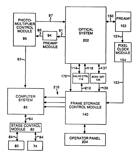
Figure 2 depicts a simplified block diagram of
the scanning laser microscope system 10 shown in Figure 1
with duplicate parts omitted for clarity. Referring to
Figure 2, the system 10 includes an optical system 202 (as
described above), the preamplifying module 94, the
photomultiplier control module 96, the computer system 86,
the stage cont-ol module 82, the scanning stage keypad and
display unit 80, the scanning stage assembly 74, the galvo
control module 116, the scan detection circuit 136, the
preamplifier circuit 152, the pixel clock module 154, the
frame storage control module 140, and an operator panel
204.
~he optical system 202, specifically the light
sensor 148 within the optical system 202, is connected by
the cable 150 for sending signals to and for receiving bias
voltage from the preamplifier circuit 152. The
preamplifier circuit 152 is connected by the line 151 for
sending signals to the pixel clock module 154. The pixel
clock module 154 is connected by the line 153 for sending
signals to the frame storage control module 140.
The optical system 202, specifically the dual
photo sensor 132, is connected by a cable 137 for sending
signals to and for receiving bias voltage from the scan
detection circuit 136. The scan detection circuit 136 is
connected by the line 138 for sending signals to the frame
storage control module 140.
The optical system 202, specifically the
position sensor 112, is connected by the cable 114 for
3~ sending signals to and for receiving bias voltage from the
galvanometer control module 116. The galvanometer control
module 116 is connected by the cable llB for sending drive
-17-
2~J~?5~0
-18-
current to the galvanometer assembly 58. The galvanometer
control module 116 is also connected by a line 210 for
receiving signals from the frame storage control module
140.
The optical system 202, specifically the start
of rotation detector 174, is connected by the cable 176 for
sending signals to and receivin~ power from the frame
storage control module 140.
The optical system 202, specifically the
photodetector assembly 90, is connected by the line 91 for
sending signals to the preamplifying module 94 which in
turn is connected by the line 95 for sending signals to the
photomultiplier control module g6. The photomultiplier
control module 96 is connected by the line 97 for sending
control voltage to the optical system 202, specifically the
photodetector assembly 90. The photomultiplier control
module 96 is als~ connected by the line 93 for sending
detected light or VIDEO signals to the computer system B6.
The computer system 86 is connected by a cable
84 for communicating with the stage control module B2 which
in turn is connected by cables B4 to the scanning stage
assembly 74 and the scanning stage keypad and display unit
80. The computer system 86 is also connected by lines 216
for receiving signals from the frame storage control module
140.
The frame storage control module 140 is also
connected by lines for sending signals to and for receiving
signals from an operator panel 204.
Referring to Figure 3, there is illustrated a
detailed side view of a modified microscope base 300 with
certain parts shown in section and other parts omitted for
clarity as used in the preferred embodiment of the present
invention. The base 300 has a lower portion 302 connected
to an upper portion 304 by an intermediate portion 306.
The photodetector assembly 90 is mounted partially recessed
in a hole 30B in the lower portion 302. The upper portion
304 has a top surface 310. A track 312 is connected to the
-18-
2i}(.~(l s~
--19--
top surface 310, such as by one or more screws 314. The
track 312 is for supporting the third, fourth and fifth
biconvex lenses 60, 62 and 64.
Any means can be used to support the lenses on
the track 312. Figure 3 shows lenses 60 and 62 held in
cylindrical lens holders 316 by retaining rings 318 such as
a c-ring. ~eferring to Figure 3, the lens holders 316 are
connected to a cylindrical support 320 by set screws 322.
Lens 64 is held in a cylindrical support 330 by retaining
rings or pieces 323. The supports 320 and 330 are
connected to clamps 324 by screws 326. The clamps 324 are
positionable along and connect to the track 312. When
either one of the clamps 324 is moved along the track 312,
a head of one of the screws 326 holding the support to the
clamp 324 moves in a clearance slot 328 in the track 312.
The mirror or beam splitter 66 is supported
within a cylindrical wall 336 having an opening 33B and a
lower flange 340. The cylindrical wall 336 surrounds a
pascage 392. The flange 340 rests on a dovetail holding
fixture 344 around the passage 342. A passage 346 in the
upper portion 304 connects the passage 342 to the plano-
apochromat microscope objective lens 68. The lens 68 can
~e one of a plurality of lenses on a rotata~le turret
assembly 348. A spacer ring shaped block 350 fits around
2~ the cylindrical wall 336 and on the flange 340. A housing
352 is positioned on the spacer block 350 over the mirror
66. Screws 356 connect the flange 340, the spacer block
350 and the housing 352 together. The thicknesses of the
fixture 344 and the block 350 and the flange 340 are chosen
to align the mirror or beam splitter 66 to intercept the
beam 24 from the lens 64 and direct it to the plano-
apochromat microscope objective lens 68. The top surface
310 of the ~ase 300 can have different levels to help align
the parts. For instance, in Figure 3 the top surface 310
3~ has a lower portion in which the fixture 344 is partially
recessed and a higher portion upon which the track 312 is
mounted.
-19-
21i~`'CP5:~,0
-20-
A second enhancing assembly BB can be located
above the beam splitter 66 to receive light reflected from
the object after the reflected light has passed through the
passage 346, the passage 342 and the beam splitter 66. The
preferred embodiment for this second enhancing assembly B8
is illustrated in Figure 6~. Another photodetector
assembly 90' is positioned to receive the reflected light
from the second enhancing means B8. The another
photodetector assembly 90' can be identical to the assembly
90. ~rther, the signal from the assembly 90l is similarly
sent to a preamplifying module 94" ~like modules 94 and
94'), a photodetector control module 96" (like modules 96
and 96') and then the computer system B6, specifically, for
instance, to a frame buffer 27B.
Referring to Figure 3A, there is shown a side
view of a microscope, such as available from E. Leitz,
Incorporated, under model name Ergolux, that can be
modified for use as illustrated in Figure 3. The
microsoope includes the lower portion 302 with the hole
308. A light source (nG~ depicted) and a mirror 360 are
typically mounted in the lower portion 302 and aligned to
direct light from the light source through a lens 35B
. mounted in the hole 308. For the purposes of the present
invention, the light source, the mirror 360 and the lens
358 can be removed and then the photodetector assembly 90
is mounted partially recessed in the hole 308.
The microscope further includes an illumination
. assembly 362, a filter assembly 364 and the housing mounted
. on t~e top portion 304 of the base 300. For the purposes of
the present invention, the illumination assembly 362 and
the filter assembly 364 are removed, the top surface 310 is
machined flat to accept track 312, and the housing 352 is
repositioned as described above.
~he microscope further includes a stage assembly
368 and a top and eye piece 366 which can be removed for
the purposes of the present invention. ~he computer
-20-
2~ 5~
-21-
controllable scannin~ stage assembly ~4 described before
can be substituted for the typical sta~e assembly 36B.
Referring to ~igures 4 and 4A, there is
illustrated a first embodiment BB' of the beam enhancing
assembly 88 in accordance with the present invention. This
first beam enhancing assembly 8B' comprises a lower housing
900 having a cylindrical opening or passage 402 for
receiving and rotatably mounting on the photodetector
assembly 90. A thumb screw 404 is provided to threadably
pass through a hole in the lower housing 400 to fasten the
housing 400 to the assembly 90.
The housing 400 has a slot 406 for receiving a
light shield or support plate 408 linearly slidable in the
slot 406. A track piece 410 extends in and is slidable
through a generally rectangular hole 412 in the support
plate 408. A ring or holder seat 41q is bonded in a slot,
such as by epoxy, at one end of the track piece 410 that
extends into the lower housing cylindrical opening 402.
The ring 414 sets in a groove around a cylindrical filter
holder 416 which is rotatable in the ring 414. A spatial
filter 41B rests in notches in one end of the filter holder
416. A C-ring 420 holds the filter 41B in the holder 416.
The spatial filter 418 has an aperture shaped to
substantially match a uniform intensity level area in an
interference pattern formed when linearly polarized
substantially monochromatic light is transmitted through
the object 70. In one preferred embodiment the spatial
filter 418 can ~e a metal reticle having a cross or plus
shaped aperture. Suitable for use is metal reticle 70.1045
from Rolyn Optics Company of Covina, California.
An actuating wire or member 422 is slida~ly
positioned in a groove in the track piece 410. A first end
of the actuating wire 422 connects to the filter holder
416. A second end of the wire 422 is bonded, such as with
epoxy in a hole of a slider 424 which is also slidably
positioned in a groove of the track piece. The first end
of the wire 422 is connected to the filter holder 416 by a
-21-
2~ t~.0
-22-
hook in the wire fitting into a hole in holder 416. The
grooves in the track piece 410 and the wire 422 are
angularly shaped such that when the slider 424 is moved
towards the wire 422 the first end of the wire 922 is
pushed generally in a direction that it is angled from a
longitudinal axis of the track piece 410.
A retaining plate 426 and a clamp 428 are
fastened to the track piece 410 by screws 430 covering part
of the wire 422 and the slider 424. An upper housing 432
connects to the lower housing 400 by screws 434. The upper
housing 432 has a cylindrical passage 436 which is
concentric with the lower housing opening 402 when
connected together.
A screw 438 is retained in the slider 424 by a
retaining collar 439 bonded to the screw 438. The screw
438 threadably engages the clamp 428 such that when the
screw 438 is turned the slider 424 and the wire 422 slide
in the groove of the track piece 410. This in turn mo~es
the end of the wire 422 connected to the holder 416
rotating the holder 416 in the ring 414.
A slidable holder 440 slidably rests in a groove
of the lower housing 400. A screw 442 passes through a
biasing spacer 444, a washer 446, and a support bracket
448. Then the screw 442 engages a retaining collar 450
that is bonded to the screw 442. ~he screw 442 then passes
through the slidable holder 440 and is threadably connected
to the clamp 428. When the screw 442 is turned, it moves
the clamp 428, the track piece 410, the support plate 408
ln the slot 406, the ring 414, the holder 416 and the
filter 418, all as a single structure in a first linear
direction.
A screw 452 passes through a biasing spacer 454,
a washer 456, and an end plate 45B which is secured to the
lower housing 400 by screws 462. Then the screw 452
engages a retaining collar 460 ~that is bonded to the screw
452). ~hen the screw 452 passes through the end plate 458
and is threadably connected to the slidable holder 440.
2`1~?~
--23--
Thus, when the screw 452 is turned, it moves the holder
440, the clamp 428, the track piece 410 through the hole
412, the ring 414, the holder 416, and the filter 41B, all
as a single structure in a second linear direction which is
perpendicular to the first linear direction.
A polarizing filter holder 464 is fastened in
one end of the upper housing passage 436 by a thumb screw
466. A polarizing filter 468 is held in a passage of the
filter holder 464 by a C-ring.
The first beam enhancing assembly 88', as just
described and illustrated in ~igures 4 and 4A, is capable
of passing light rays through the variably positionable
cross shaped opening and blocking all other light rays from
the assembly 90. Further, the filter 418 is adjustably
positionable in two perpendicular linear directions and in
an angular direction.
The assembly 8B' is particularly useful when
detecting light from a birefringent object and more
particularly a birefringent, partially transparent object.
The cross shape of the aperture in the filter 41B allows a
large uniform porti~n of a typical light interference
pattern caused by passing polarized light through a
birefringent material to be detected by the assembly 90.
~he portion of light that passes through the cross shaped
aperture has been found to contain increased anomally
information concerning the object structure which produces
remarkably clear signals detectable by the assembly 90 as
compared to prior art microscopes including prior laser
scanning microscope systems.
Referring to Figures 5 and SA, there is
illustrated a second embodiment 8B'' of the ~eam enhancing
assembly 88 in accordance with the present invention. This
second beam enhancing assembly 88'' has a longitudinal axis
501 and comprises, from bottom to top, a base S00, a
rotatable holder 502, a spatial filter plate, 504, a
rotatable disk 506, a support 508, a filter holder S10, and
a polarizing filter 512.
-23-
2~
-24-
The base 500 has a cylindrical passage 514 for
rotatably mounting on the photodetector assembly 90. A
thumb screw 516 can fix the base 500 to the assembly 90.
The passage 514 has a shoulder 518 for receiving a lower
portion 520 of the holder 502.
The holder 502 is generally shaped as a disk
having a lower portion 520; a middle portion including
circumferential grips 522, an annular groove 524, an
optical aperture 526 and an off center pin 528 extending
up; and an upper ring portion 530. A thumb screw 55~ fixes
the base 500 to the holder S02.
The spatial filter plate 504 has an off center
hole 532 for receiving the pin 528. The plate 504 further
has an upper radial groove 536 and a~ optical aperture 534,
which is smaller than the holder optical aperture 526, for
aligning above the holder optical aperture 526. The filter
plate aperture 534 can be any shape desired, but for
purposes of illustration it is depicted as circular. The
filter plate 504 is smaller than the holder 502, such that
when the pin 528 of the holder 502 is in the hole 532 of
the filter plate 504, the filter plate 504 does not extend
radially to the annular groove 524 through most of the
filter plate's rotation about the pin 528 and the filter
plate 504 does not extend above the ring portion 530. A
nylon tipped set screw 523 can be used to increase friction
between the holder 502 and the rotatable disk 506.
The rotatable disk 506 has circumferential grips
and an optical aperture 53B larger than and alignable above
the filter plate aperture 534 and the holder aperture 526.
The disk 506 further has an off center downwardly
projecting pin 540 and a lower shoulder 542 with a
downwardly projecting tang 544 on the shoulder 542.
Although the tang 544 is illustrated in Figure 5, in
reality the tang 544 would not been seen in the Figure 5
perspective. In Figure 5, the tang 544 is actually
connected to the shoulder 542 about at the point farthest
from the viewer. The pin 540 extends into the filter plate
-24-
2i~(?(~
-2S-
radial groove 536. The tang 544 extends into the holder
annular groove 524.
The support 50B has a cylindrical passage 554
coaxial with the base passage 514 and alignment holes 548
for receiving locating pins 546 on the base 500. Screws
550 secure the support 508 to the base 500. The base 500
has a step 552 for providing a space between the support
508 and the remainder of the base 500 for rotatably
trapping the holder 502, the plate 504 and the disk 506
therebetween.
A polarizing filter 558 in a holder 560 is
secured by a thumb screw 562 within the support passage
554.
When the holder 502, the filter plate 504 and
the disk 506 are stationary, the passage of light through
the assembly B~'' is limited by the filter plate aperture
534 because it is the smallest one of the three apertures.
Further, the spatial or optical apertures 538, 534, and 526
are always aligned permitting light to pass through the
filter plate aperture 534 regardless of where it is
: located. The position of the filter plate aperture 534 is
moved by rotating the assembly 8B'' with res~ect to the
: assembly 90 or by rotating one or both of the disk 506 or
the holder 502 with respect to the base 500.hhen the disk 506 is rotated clockwise looking
down in Figures 5 and 5A until it stops rotating with
respect to the holder 502, the filter plate aperture 534 is
symmetric about the axis 501 of the assembly B8'', the tang
544 is ~t a first end of the annular groove 524, and the
pin 540 is close to the axis 501. From this position, if
the disk 506 is rotated countercl~ckwise looking down in
Figures 5 and SA with respect to the holder 502, the filter
plate aperture 534 moves in an arc away from the axis 5~1,
the tang 594 moves along the annular groove 524 away from
its first end towards its second end, and the pin 53B moves
along the groove 53Ç away ~rom the axis 501. The disk 506
stops rotating counterclockwise with respect to the holder
: -25-
:
2I~
--26--
502 when the tan~ 544 contacts the second end of the
annular groove 524. At any position of the filter plate
aperture 534 along the arc, the disk 506 and the the holder
502 can be rotated in unison to cause the filter plate
5 aperture 534 to rotate about the axis S01.
The second beam enhancing assembly 88'', as just
described and illustrated in Figures 5 and SA, is capable
of bloc~ing light from enterin~ into the photodetector
assembly 90, except for light rays passing through the
optical apertures 538, 534, and 526. Like the enhancing
assem~ly 88', the enhancing assembly 88" is particularly
useful when viewing a birefringent object. In addition,
this assembly B8" is particularly useful in detecting rays
caused by absorptive foreign bodies in the object and
scattering anomalies.
Referring to Figures 6 and 6A, there is
illustrated a third embodiment 88''' of the beam enhancing
assembly 88 in accordance with the present invention. This
third beam enhancing assembly 88''' comprises a base 602
including a cylindrical portion 604 for mounting on the
photodetector assembly 90. The cylindrical portion 604 is
connected to a support plate portion 606 having a circular
passage 608 through it about an axis 610 for allowing light
to enter the photodetector assembly 90.
An iris diaphragm assembly 612, such as assembly
model no. 75.0175 from ~olyn Optics Company, is on the
support plate portion 606. The iris diaphragm assembly 612
includes a frame 614 from which a shutter or iris diaphragm
616 extends to and from the axis 610 providing a variable
aperture with a diameter that is adjustable by an actuating
arm 618.
A cylindrical housing 620 with a window 622 and
open ends is connected at one of its ends to the plate
portion 606. A sleeve support 624 is positioned within the
housing 620. The sleeve support 624 has two ends, an
internal upper shoulder 626 and an internal lower shoulder
628. One of the ends of the sleeve support 624 contacts
-26-
Z~}(~
-27-
the plate portion 606. The iris diaphragm assembly 612 is
held in position by and between the internal lower shoulder
62B and the internal lower shoulder 628. The sleeve
support 624 has a recess 630 in its outer surface and a
S hole 632 in the recess 630. The recess 630 is aligned with
the window 622. The cylindrical housing 620 can be secured
to the base 602 by screws, epoxy or any other suitable
means. The sleeve support 624 can be secured to the
housing 62~ by screws, epoxy or any other suitable means.
A rod or arm 634 passes through the window 622,
the recess 630 and the hole 632 such that a first end of
the rod 634 extends inside the sleeve support 624 and a
second end of the rod 634 extends outside the cylindrical
housing 620. The first end of the rod 634 supports a light
blocking black disk or member 636 ~enerally perpendicular
to the axis 610. The disk 636 can be circular in shape. A
grip 638 is attached to the second end of the rod 634. The
sleeve support 624 includes a rod or arm support 640 which
extends through the window 622 and into the recess 630 and
is mounted on the sleeve support 624 by pairs 642 of screws
and washers. The rod 634 is slidably supported in a
passage, in a light tight manner, in the support 640. Arms
644 of the support 640 positioned above and below the grip
638 prevent the rod 634 from rotating.
A first biconvex lens 646 is supported on the
internal upper shoulder 626 of the sleeve support 624. A
cylindrical spacer 648, which can be any material such as
plastic, is positioned inside and contacting the sleeve 624
on the first biconvex lens 646. A second biconvex lens 650
rests on the spacer 648. An annular reta$ning plate 652 is
mounted to the top end of the sleeve 624 by screws 654 to
secure the lenses 646, 650 and spacer 648 within the sleeve
624.
The third beam enhancing assembly 88 " ', as just
described and illustrated in Figures 6 and 6A, is
particularly useful for detecting light scattered by the
object 70. The disk 636 is linearly positionable within
-27-
2~ a
-28-
the sleeve 624 by moving the grip 638. The disk 636 is
angularly positionable within the sleeve 624 by rotating
the base 602 with respect to the assembly 90. As such, the
disk 636 and the iris diaphragm 616 can be positioned so
S that light which is unaffected by the object 70 will be
blocked and not pass to the assembly 90. In such a case,
light scattered by the object will be detected by the
assembly 90. The disk 636 and the iris diaphragm 616 can
be positioned with respect to each other such that an
annular or ring shaped aperture is jointly defined by the
disk 636 and the iris diaphragm 616.
Referring to Figure 6B, t~ere is illustrated a
fourth embodiment 88'''' of the beam enhancing assembly 88
in accordance with the present invention. This fourth beam
enhancing assembly 88'''' comprises a base 680 including a
cylindrical portion for mounting on the photodetector
assembly 90'. The cylindrical portion is connected to an
annular supp~rt plate portion.
One end of a cylindrical wall 670 is connected
to the annular support plate portion of the base 680.
Another iris diaphragm or spatial filter assembly 612, like
the one described in relation to Figures 6 and 6A, is
located in the cylindrical wall 670 adjacent the base
annular support plate portion.
The other end of the cylindrical wall 670 has a
ring shaped projection 672 for inserting into a recessed
area of the housing 352. See Figure 3.
The cylindrical wall 670 has an internal
shoulder 674 near its other end, the end with the
projection 672. A biconvex lens 676 is held against the
shoulder 674 by a holder 678, such as a C-ring. The lens
676 is positioned to focus light reflected from the object
70 through the variable aperture of the iris diaphragm
assembly 612 to an area on the photomultiplier tu~e 682 of
the photodetector assembly 90'. As mentioned before, the
signal representative of light reflected from the object is
sent to a preamplifying module 94" ~not depicted), to a
-28-
2~1('510
-29-
photodetector control module 96~ (not depicted) and then
the computer system 86, specifically, for instance, to the
frame buffer 278.
The fourth beam enhancing assembly 88' " ' allows
a greater amount of light reflected from the object 70 to
be detected than through use of the confocal arrangement
previously described in relation to Figure 1.
Referring to Figure 6C, there is illustrated a
fifth embodiment B8''''' of the beam enhancing assembly 88
in accordance with the present invention. This fifth beam
enhancing assembly 8~''''` is the same as the fourth beam
enhancing assembly 88'''' as described above, except a
wavelength selective filter is secured between the object
and the photomultiplier tube instead of an iris diaphragm
assembly.
More specifically, the fifth beam enhancing
assembly B8''''' comprises a base 605 including a
cylindrical portion 607 for mounting on the photodetector
assembly 90'. The cylindrical portion 606 is connected to
an annular support plate portion 609.
one end of a tubular connector or housing 611 is
connected to the annular support plate portion 609 of the
base 605. A wavelength selective filter assembly 613 is
located in the tubular connector 611 between a biconvex
lens 619 and the photomultiplier tube 682. The wavelength
selective filter assembly can comprise a first band pass
filter assembly 613 adjacent the photodetector assembly
90', a second band pass filter assembly 635 adjacent the
lens 619 and~or a dichroic beam splitter assembly 633.
A second end of the tubular connector 611 has a
r~ng shaped projection 615 for inserting into a recessed
area of the housing 352. See Figure 3.
~he tubular connector 611 has an internal
shoulder 617 near its second end. The biconvex lens 619 is
held against the shoulder 617 by a holder 621, such as a C-
ring. The lens 619 is positioned to focus light reflected
from the object 70 through the wavelength selective filter
-29-
2I~(t`510
-30-
613 to an area on the photomultiplier tube 682 of the
photodetector assembly 90'. As mentioned before, the
signal representative of light reflected from the object is
sent to a preamplifying module 94" (not depicted), to a
photodetector control module 96" (not depicted) and then
the computer system 86, specifically, for instance, to the
frame buffer 27B.
The tubular connector 611 can have a third end
connected to an annular support plate portion 623 of a base
625. Another band pass filter assembly 627 can be located
in the tubular connector 611 adjacent the base annular
support plate portion 623. The base 625 has a cylindrical
portion 629 for mounting on a photodetector assembly 90''
including a photomultiplier tube 631 which is electrically
connected to a preamplifying module 94''' (not depicted),
then to a photodetector control module 96''' (not depicted)
and then to the computer system 86, specifically, for
instance, to the frame buffer 278.
~he dichroic beam splitter assembly 633 allows
wavelengths either above or below a certain wavelength to
pass through the dichroic beam splitter assembly 633
through the band pass filter assembly 613 to an area on the
photomultiplier tube 682 of the photodetector assembly 90'
and reflects all other wavelengths through the band pass
filter assembly 627 to an area on the photomultiplier tube
; 631 of the photodetector assembly 90''.
Referring to Figure 6D, there is illustrated a
sixth embodiment 88'''''' of the beam enhancing assembly 88
ln accordance with the present invention. ~his sixth beam
enhancing assembly 88'''''' comprises a base 641 including
a cylindrical portion 643 for mounting on the photodetector
assembly 90'. The cylindrical portion 643 is connected to
an annular support plate portion 645.
A wavelength selective filter assembly, such as
a band pass filter assembly 647, is connected to the
annular support plate portion 645. the band pass filter
assembly 647 comprises a housing 647, a disk 651 rotatable
-30-
2~?~?51~
about an axis, a plurality of band pass filters 653 mounted
in the disk 651 at an equal radial distance from the disk
axis of rotation, and a motor assembly 655 supported by the
housing 647 to rotate the disk 651 within the ~ousing 647
to selectively position any one of the band pass filters
653 in the path of light detected by the photodetector
assembly 90'. Each of the filters 6~3 permits a different
range of light wavelenths to pass through $t and blocks all
other wavelengths. A suitable band pass filter assembly
647 can be purchased under model number 77371 from Oriel
Corporatio~ with offices in Statford, Connecticut. The
motor assembly 655 can be connected to the computer system
86 such that an operator can select by inputting through a
keyboard the particular band of light wavelengths desired
to be detected by the photodetector assembly 90', thus,
selecting and rotating the corresponding filter 653 to be
p~sitioned in front of the photodetector assembly 90'.
One end of a cylindrical wall 657 is connected
to the housing 647. The other end of the cylindrical wall
657 has a ring shaped projection 659 for inserting into a
recessed area of the housing 352. See Figure 3.
The cylindrical wall 657 has an internal
shoulder 661 near its other end, the end with the
projection 659. A biconvex lens 663 is held against the
shoulder 661 by a holder 665, such as a C-ring. The lens
663 is positioned to focus light reflected from the ob~ect
70 through the selected filter 653 of the filter assembly
647 to an area on the photomultiplier tube 682 of the
photodetector assembly 90'. As mentioned before, the
signal representative of light reflected from the object is
sent to a preamplifying module 94" (not depicted), to a
photodetector control module 96" (not depicted) and then
the computer system 86, specifically, for instance, to the
frame buffer 278.
~he fifth and sixth beam enhancin~ assemblies
88''''', 88'''''' are used for luminescence microscopy.
The emission of light by certain objects is called
2'~ 10
luminescence. There are different kinds of luminescence.
~irst, fluorecence is light which is emitted practically
simultaneously with the introduction of an excitation
energy and which ceases as soon as the exciting radiation
ceases. Second, phosphorescence is light which is emitted
and persists some time after excitation is removed. For
$nstance, laser 20 or laser 156 can be chosen to emit a
beam 24 of light that stim~lates, excites or causes an
object 70 or particles in an object to fluoresce or emit
light. The wavelength selective filter assemblies 613 and
647 are chosen to block aIl light from passing throu~h them
including the wavelength(s) of t~e laser beam 24 and allows
only the fluorescent wavelengths being excited and emitted
by the object to be detected by the correspondin~
photodetector assembly. Furthermore, laser 20 and laser
156 can be chosen to simultaneously emit beams of light
that stimulate, excite or cause an object 70 or particles
in an object to fluoresce or emit different wavelengths of
light. These different wavelengths can be simultaneously
or sequentially detected by different photodetector
assemblies in the same enhancing assembly 88, such as in
enhancing assembly 88''''', and/or by different
photodetector assemblies in different enhancing assemblies
88, such as having an enhancing assembly 88''' " connected
between the photodetector assembly 90' and the housing 352
in Figure 3 and a second enhancing assembly 88" '''
connected between the photodetector assembly 16B and the
beam stop 166 in ~igure 1.
Thus, the scanning laser microscope system 10
may serve the additional function of exciting fluorescent
molecules in the object 70. When used for florescence
microscopy, the light detected by the photomultlplier tube
and the image formed represent only the fluorescent portion
of the object. Since only very specific wavelengths will
be absorbed or emitted by a particular fluorescent
molecule, such as a fluorophore, the laser and the
2~ 510
-33-
wavelength selective filters must be chosen to allow
detection of the emitted fluorescence.
The object 70 may be of biological or other
origin. The fluorescence may be due to fluorophores
naturally present in the object, or the object may be
treated with fluorescent molecules to label desired
components in the sample. Other types of luminescence,
such as, bioluminescence and chemiluminescence, do not
requ~re excitation by a light source to emit light.
1~ The scanning laser microscope system 10 in
fluorescence mode may be used for the detection,
enumeration, and analysis of fluorescently labeled
bacteria, yeast, molds, and microbial spores. Any method
that fluorescently labels microorganisms may be used,
including treatment with direct fluorescent reagents,
fluorescent tagged antibodies or lectins for
immunofluorescence or lectin fluorescence assays, or
fluorescent vital stains as indicators of viability.
Eluorescently labeled microorganisms may be placed on any
appropriate surface for scanning.
Microorganisms isolated from food and beverage
samples, sanitation swabs, or clinical samples such as
urine may be fluorescently labeled for detection,
enumeration, and/or determination of viability. This
approac~ may be used in place of, or in addition to,
traditional methods, including growing microorganisms on
selective, nutrient media and other
physiological/biochemical methods.
Furthermore, the word anomalies as used herein
is intended to include to include fluorescent molecules,
particles or materials of biological or non-biological
ori~in.
~ wo Examples are provided below. Example 1 is
provided to show that in its fluorescence mode the scanning
laser microscope system 10 may ~e used for detection,
enumeratio~, and analysis of microorganisms directly
stained with a fluorescent reagent. Example 2 is provided
-33-
21~Q~510
-34-
to show that specific microorganisms in a sample may be
fluorescently labeled and then detected, enumerated, and
analyzed using the scanning laser microscope system 10 of
the present invention.
EXAMPLE 1
An aliquot of a yeast culture such as Candida
vini (available from American Type Culture Collection
(ATCC), under ATCC number 18823, Rockville, Maryland) in
nutrient Bacto YM broth (available from Difco Laboratories,
Detroit, MI) was vacuum filtered onto a black polycarbonate
filter (available from Nuclepore Corporation, Pleasanton,
California). The filter is rinsed with several milliliters
(mls) of 0.2 molar (M) phosphate buffered saline (PBS), pH
7Ø The vacuum was removed, and the filter was overlayed
with a fluorescent stain, acridine orange (available from
Sigma Chemical, St. Louis, MO) (50 micrograms (~g) per ml
of PBS, pH 7.0), for 15 minutes. Vacuum was reapplied, and
the filter was rinsed in succession with several mls of
PBS, 100% iso-propanol to remove excess stain bound to the
filter, and again with PBS. The filter was air-dried and
placed on top of a glass microscope slide with a drop of
non-fluorescent immersion oil and a cover slip.
An argon ion laser 156 operating at 488
nanometers ~nm) wavelength scanned the sample. A long pass
absorbance filter 613 with a sharp cut-off at 530 nm,
number 51300 from Oriel Corporation, Stratford, Conn., was
placed before the photomultiplier tube (PMT) 682 to absorb
the reflected laser light and pass the fluorescence light.
~ his Example 1 shows that a culture may be
directly stained with a fluorescent reagent, such as a
vital stain which may be an indicator of cell viability,
and that direct staining of microorganisms may be used for
detection, enumeration, and analysis of microorganisms in a
sample using the scanning laser microscope system 10 of the
present invention.
-34-
2~ 51~)
EXAMPLE 2
In an indirect immunofluorescence assay (IFA), a
target microorganism is labeled with a primary, non-
conjugated antibody specific for microorganisms containing
the target surface antigen. Microorganisms with bound
antibody are fluorescently labeled using a fluorescein
lsothiocyanate-conjugated (FITC) secondary antibody which
recognizes the primary antibody. The labeled
microorganisms may be placed on an appropriate surface and
imaged using the scanning laser microscope. As in Fxample
1, an ar~on ion laser 156 operating at 488 nm wavelength
scans the sample. A long pass absorbance filter 613 with a
sharp cut-off at 530 nm, number 51300 from Oriel
Corporation, is placed before the PMT 682 to absorb the
reflected laser li~ht and pass the fluorescence light.
The success of this method is largely dependent
on the selectivity and cross-reactivity of the antibodies
used. Primary and secondary antibodies with low affinity
may prevent enough FITC-conjugated secondary antibody from
binding to allow for detection of labeled microorganisms.
Antibodies with high cross-reactivity will cause a high
background fluorescence, thus decrease the probability of
selectively detecting the desired microorganisms.
To show that microorganisms labeled with FITC-
con~ugated antibodles could be detected with the scanning
laser microscope system 10, a sample of yeast cells was
directly stained with FITC reagent and scanned. A 10 ml
sample of a yeast culture Torulopsis sonorensis (ATCC
number 56511, American Type Culture Collection, Rockville,
Maryland) grown overnight in nutrient YM broth (available
from Difco Laboratories~ was placed in a 15 ml centrifuge
tube. The culture was centrifuged for 10 minutes at 3000 g
to form a yeast pellet. The eluent was removed, and the
pellet resuspended in 10 ml of 0.1 M carbonate/bicarbonate
-35-
2`i~?~51~)
-36-
buffer, pH 9.2. The yeast sample was washed in this manner
3 times.
Two ml of the resuspended yeast cells were
placed in a second 1~ ml centrifuge tube, mixed with 0.4 ml
of ~ITC reagent (10 milligrams ~mg) per ml of 0.1 M
carb~nate/bicarbonate buffer, pH 9.2), and ~ept in the dark
for 30 minutes. Excess FITC was removed by washing 3 times
with 2 mls of the buffer by centrifugation. ~he ~ITC-
labeled yeast cells were vacuum filtered onto a black
polycarbonate filter (available from Nuclepore Corporation)
and washed with 10 ml of the ~uffer. The filter was air-
dried and placed on top of a glass microscope slide with a
drop of non-fluorescent immersion oil and a cover slip.
An argon ion laser 156 opera~ing at 488 nm
1~ wavelength scanned the sample. A lon~ pass absorbance
filter 613 with a sharp cut-off at 530 nm, number ~1300
from Oriel Corporation, was placed before the PMT 682 to
absorb the reflected laser light and pass the fluorescence
light.
~he FI~C-labeled yeast cells were successfully
imaged on the scanning laser microscope system 10. Since
FITC is a common light emitting tag being bound to the
antibody in an immunofluorescence assay or a lectin in a
lectin fluroescence assay, specific microorganisms in a
2~ sample may be detected, enumerated, and analyzed using
assays in which microorganisms are labeled with antibodies
or lectins conjugated to a light emitting tag, such as
FITC, with the scanning laser microscope system 10 of the
present invention.
Any one of the above described enhancing
assemblies 88', 88'', 88''', 88"'', 8B''''' and 88''''"
can be connected in the position illustrated in Figure 1
for the enhancing assembly 88, in which case the assembly
3~ B8 receives light transmitted through and emitted from the
object 70. In addition, any one of the above described
enhancing assemblies 8B', BB'', 88''', 88'''', B8''''' and
2;~ s~0
-37-
88'''''' can be connected between the photodetector
assembly 90` and the housing 352 as illustrated in Figure
3, in which case the assembly 88 receives light reflected
and emitted from the object 70. In addition, any one of
the above described enhancing assemblies 88', 88'', 8B''',
~B````, BB`'''' and 88'''''' can be connected between the
photodetect~r assembly 168 and the beam stop 166 ~see
Figure 3), in which case the assembly B8 receives light
reflected and emitted from the object 70 in a confocal
arrangement.
Referring to Figure 7, there is illustrated a
preferred embodiment of the preamplifier circuit 152
capable of use in the system of Figures 1 and 2. The
purpose of the preamplifier circuit 152 is to convert a ~-
current mode output of the photodetector 14B into a voltage
signal of a level useable by the pixel cloc~ module 154.
Alth~ugh the circuit of Figure 7 is a preferred embodiment,
any circuit that serves this purpose can be used. When the
preamplifier circuit 152 depicted in Figure 7 is used, the
photodetector 14B is operated in a reverse biased mode as
is well known in the art. This preferred preamplifier
circuit 152 is similar to and can be further understood by
reference to the circuit particularly described in
Integrated Circuits Data Handb~ok, Burr-Brown Corporation,
Chapter 1, page 189, 198~.
The preamplifying module 94 can be similarly
configured to the aforedescribed preamplifier circuit 152.
However, in Figures 1 and 2, the photomultiplier module 96
provides the high voltage to the photodetector assembly 90.
One skilled in the art having this disclosure before him
can desi~n numerous preamplifying circuits or modules
capable of use for circuit 152 and module 94 in the present
system.
Figure B depicts a preferred embodiment of the
scan detection circuit 136 suitable for use in the system
; of Figures 1 and 2. For a detailed description of this
scan detection circuit, see Laser Applications, Volume 4,
2~}(,~
-38-
edited by Goodman and Ross, pages 171-173, 1980. The
circuit depicted in Figure 8 illustrates a preferred
embodiment of the scan detection circuit useable in the
present invention. ~owe~er, any circuit may be used as
long as it can provide signals to the frame storage control
module 140 indicating the precise position of the beam 24
on the object 70 at the beginning of each scan of the beam
across the object.
~igu~e 9 is a sc~ematic representation of the
frame storage control ~odule 140 and the operator control
panel 204 of Figure 2. One purpose or function of the
frame storage control module 140 is to generate control
signals to synchronize a digital frame storage unit 271 in
the computer system 86 to the actual position of the beam
lS on the object. Based on the control signals from the frame
storage control module 140, the digital frame storage unit
271 samples, diqitizes and stores the detected signal from
the photodetector assembly 90 at precisely spaced
intervals. The digital signals are stored in memory
locations corresponding to the position of the beam 24 on
the object 70. Another purpose of the frame storage
control module 140 is to generate a beam position reference
signal to be used hy the galvo control module 116 which
adjusts the drive current to the galvanometer 56 to cause
the actual beam position to accurately track the beam
reference signal.
The frame storage control module 140 comprises a
frame storage control circuit 226, a scan-l circuit 242, a
scan-2 circuit 244, and a scan-3 circuit 246. The frame
storage control circuit 226 is connected to the scan-l
circ~it 242 by four lines 248, three of the lines 248 are
for sending signals from the frame storage control circuit
to the scan-l circuit 242, one of the lines 248 is for
sending signals from the scan-l circuit 242 to the frame
storage control circuit 226. T~e scan-l circuit 242 is
connected to the scan-2 circuit 244 by three lines 250, two
for sending signals from the scan-2 circuit 244 to the
-38-
2 ~ `510
-39-
scan-l circuit 242, one for sending signals from the scan-l
circuit 242 to the scan-2 circuit 244. A line 252 connects
one of the lines 250 (which is for sending signals from the
scan-2 circuit 244 to the scan-l circuit 242) to the frame
or image storage control circuit 226 for sending signals
from the scan-2 circuit 244 to the frame storage control
circuit 226. ~ line 254 connects the frame storage control
circuit 226 to the scan-2 circuit 244 for sending signals
from the frame storage control circuit 2~6 to the scan-2
circuit 244. A data bus 2~6 with 9 lines connects the
scan-2 circuit 244 for sending signals to the scan-3
circuit 246.
The frame storage control module 140 receives
signals or inputs over line 138 from the scan detection
circuit 136 to the frame storage control circuit 226, over
line 176 from the start of rotation detector 174 to the
frame storage control circuit 226, over line 153 from the
pixel clock module 154 to the frame storage control circuit
226, over lines 228 from controls or switches 230 on the
operator panel 204 to the scan-1 circuit 242, and over two
data ~uses 232, each having twelve signal paths or lines,
from switches 234, such as thumbwheel switches, on the
operator panel 204 to the scan-2 circuit 244. The frame
storage control module 140 sends signals over three lines
216 to the computer system 86 from the frame storage
control circuit 226, over line 116 to the galvanometer
control module 116 from the frame storage control circuit
226, and over a data bus 238 to a display 240 on the
operator panel 204 from scan-3 circuit 246.
3D Figure 10 is a detailed functional bloc~ diagram
of the frame storage control module 140 for use in the
system of Figures 1 and 2. ~eferring to Figure 10, the
frame storage control circuit 226 receives signals from the
scan detect circuit 136 and the pixel clock module 154,
hereafter called SCAN DETECT signals and PIXEL CLOC~
signals, respectively. The SCAN DETECT signals are fed
into a pulse synchronization ~sync) integrated circuit (IC)
-39-
2,~ 510
-40-
1002, such as a 74120. Clock signals are generated by a
crystal clock module 1001 such as a 5406-4M fro~ MF
Electronics of New Rochelle, New York and sent to the pulse
sync IC 1002. The pulse sync IC 1002 gates the CLOCK
signals on at an occurrence of a SCAN DETECT signal sending
the gated CLOC~ signals or pulses to a 12 bit down counting
circuit 1004, otherwise called a 12 bit divide by M counter
1004, which functions to create one output pulse for each M
input pulses. The 12 bit counter 1004 may for instance,
comprise three cascaded 4 bit counter ~Cs, such as 74F193
lCs. Data inputs to these counters 1004 are preselected
binary numbers or values which are typically selected using
pull-up resistors and switches connected to ground. When
the last of the cascaded counters 1004 has reached a count
equal to 0, it outputs a pulse to a one shot 1006 which in
turn reloads the counters 1009 to their initial or starting
count values. The pulse sync IC 1002, the counter 1004 and
the one shot 1006 function as a delay circuit 1007. The
output pulse from the one shot 1006 is fed to a power
driver IC 1008, such as a 74S140, which sends DELAYED SCAN
DETECT signals over one of the lines 248 to the scan-l
circuit 242.
In a similar fashion, a second set of devices
comprising a pulse sync IC 1010, a 12 bit counter 1012 and
a one shot 1014 function as a second delay circuit 1015
using the PIXEL CLOCK signals from the pixel clock module
lS4 in place of the CLOC~ signals to provide a pulse to
reset a horizontal drive flip-flop 1016 which turns off a
HORIZONTAL DRIVE gate signal. When the flip-flop 1016 is
reset, it provides an input to an AND gate 101B which in
turn enab~es the P~XEL CLOCK pulses to drive a ~12 count
circuit comprising a 12 bit counter 1020 and a one shot
1022. When the output of the one shot 1022 is active, it
sets t~e flip-flop 1016, thus, turning on the HORIZONTAL
DRIVE gate signal. An output of the flip-flop 1016 is fed
to a driver circuit 1024 which sends ~ORIZONTAL DRIVE
signals over one of the lines 216 to the frame ~uffer 272.
-40-
2`1~QC~510
-41-
Similarly, an output of the AND gate 1018 is fed to a
driver circuit 1026 which sends gated PIXEL CLOCK signals
to the frame buffer 272 over one of the lines 216.
The start of rotation sensor 174 is used to
ensure that each frame begins using the same facet or face
of the rotor 30. Its output signal which occurs once each
revolution of the rotor 30, is amplified in a circuit 1028
and sent to a Schmitt Trigger circuit 1030, such as a
74LS14, which converts the signal to a digital logic
signal. The digital logic signal is fed to an AND gate
1032.
The other input of t~e AND gate 1032 is driven
by a flip-flop 1034 which is set by an eight bit vertical
interval counter 1036 which counts the DELAYED SCAN DETECT
signals from the delay circuit 1007. The output of the
AND gate 1032 drives a one shot 103B which produces a
START SCAN signal which is sent over one of the lines 248
to the scan-l circuit 242. The output of the one shot
1038 also loads the vertical interval counter 1036 to its
initial value and sets a flip-flop 1040.
: When the last scan of a frame has been reached,
a SCAN CO~NT=STOP VALUE signal from the scan-2 circuit 244
over line 252 enables one input of an AND gate 1044
permitting the DELAYED SCAN DETECT signal from the delay
circuit 1007 to activate a one shot 1046. The one shot
1046, in turn, resets the flip-flop 1040, provides a STOP
SCAN signal to the scan-1 circuit 242 over one of the
lines 248, and resets the flip-flop 1034.
When the flip-flop 1040 is reset, it enables an
input to an AND gate 1042 which also receives the delayed
scan detect signals from the delay circuit 1007. This
enables the DELAYED SCAN DETECT signals to drive the
vertical interval counter 1036. When the flip-flop 1040
is set, it disables the AND gate 1042.
The output of the flip-flop 1040, also provides
a LOAD SCAN COUNT (auto mode) signal to the scan-2 circuit
244 over line 254 and to a driver 104B which in turn sends
2')(~`510
-42-
VERTICAL DRIVE signals on one of the lines 216 to the
frame buffer 272.
Figure 11 shows a detailed functional block
diagram of the scan-l circuit for use in the module of
Figure 9. Referring to Figure 11, the five input switches
230 on the operator panel 204 can be pushbuttons and are
connected to a switc~ debounce circuit 1102, such as a
MC14490, to ensure bounce free transition or signals when
the buttons 230 are actuated. The buttons 230 can ~e
named a cycle button, an auto button, a manual ~utton, a
single step button, and a reset button.
The outputs of the auto and manual ~uttons 230
set and reset a manua'~auto mode flip-flop 1104. When the
flip-flop 1104 is set (i.e., automatic mode), one of its
output signals enables an AND gate 1106. This AND gate
1106 then permits the START SCAN signal from the frame
stora~e con.rol circuit 226 over one of the lines 248 to
drive one input of an OR gate 1108 which drives a one shot
1110. The output of the one shot 1110 is a pulse which
sets a flip-flop 1112. The output of the flip-flop 1112
ena~les one input of an AND gate 1114 which then permits
the DELAYED SCAN DETECT signals to drive an input of an OR
gate 1116 which generates the SCAN COUNT CLOCK signals
sent to the scan-2 circuit 244 over one of t~e lines 250.
When the flip-flop 1104 is reset (i.e., manual
mode), the other output of the flip-flop 1104 enables an
AND gate 1118 with another input being the output from the
single step button 230. When the single step pushbutton
230 is depressed, the output of the AND gate lllB enables
a pulse synchronization (sync) circuit 1120 which produces
one output pulse when the next delayed scan detect pulse
arrives at its other input. The output of the pulse sync
circuit 1120 is sent to the other input of the OR gate
1116 to produce the scan count clock signal to be sent to
the scan-2 circuit 244. When the cycle button is
depressed, a signal is sent to the other input of the OR
gate 1108 and then to the one shot 1110. The output pulse
-42-
2~ 5~0
-43-
from the one shot 1110 sets the flip-flop 1112 which
operates as previously described.
When the reset button is depressed, its output
is sent to inputs of a first OR gate 1122 and a second OR
gate 1124. The output of the first O~ gate 1122 resets
the flip-flop 1112. The second OR gate 1124 output
generates the LOAD SCAN COUNT (manual mode) signal which
is sent to t~e frame storage control circuit 226 over one
of the lines 248. The other t~o inp~ts to the first OR
gate 1122 are the STOP SCAN signal which comes from the
frame storage control circuit 226 and the SCAN COUNT=512
si~nal which comes from the scan-2 circuit 244. The other
two inputs to the second OR gate 1124 are the STOP SCAN
si~nal from the frame storage control circuit 226 and the
SCAN COUNT=STOP VALUE signal from the scan-2 circuit 244.
Figure 12 shows a detailed functional block
diagram of the scan-2 circuit for use in the module of
Figure 9. Referring to Figure 12, three switches, such as
binary coded decimal (BCD) thumbwheel switches 234, on the
operator panel 204 are set to a desired START SCAN COUNT
value by the operator. The BCD output signals from these
switches 234 are converted to a 10 bit binary
representation by a BCD to binary converter circuit 1202.
This 10 bit representation is sent to a 10 bit ~inary
counter 1204, called a scan counter 1204. The LOAD SCAN
COUNT signal over line 254 from the frame storage control
circuit 226 permits the loading of the 10 bit
representation into the counter 1204. The counter 1204
increments each time a pulse occurs in the SCAN COUNT
CLOCK signal over one of the lines 250 from the scan-l
circuit 242. The output of the counter 1204 is sent to a
10 bit binary comparator 1206 and to the scan-3 circuit
246 over the bus 256. The most significant bit, i.e., the
bit that represents a count of 512, is sent over one of
the lines 250 to the scan-1 circuit 242.
The other input of the binary comparator 1206 is
driven by a ~inary representation of a STOP SCAN CO~NT
-43-
2`~ Sl~
signal which has been input through switches 234 and
converted to the binary representation by a BCD to binary
converter 1208 in similar fashion.
When the output of the scan counter 1204 equals
the STOP SCAN COUNT value, the output of the comparator
1206 becomes active producing a SCAN COUNT=STOP VALUE
signal which is sent to the frame storage control circuit
226 over the line 252 and to the scan-l circuit 242 over
one of the lines 250.
Figure 13 shows a detaileà functional block
diagram of the scan-3 circuit for use in the module of
Figure 9. Referring to Figure 13, the 10 bit output of
the scan counter 1204 in the scan-2 circuit 244 is sent
over the bus 256 to a 10 bit multiplying digital to analog
converter (DAC) 1302. A precision voltage reference 1304
supplies a reference input to the converter 1302. The
output of the DAC 1302 is fe~ to one input of a difference
amplifier 1306. The other input of the difference
amplifier 1306 is driven by a potentiometer 1308 which is
in turn connected to the precision voltage reference 1304.
The potentiometer 1308 provides capability to adjust the
middle point of the output of the amplifier 1306 to zero.
The output of the amplifier 1306 is sent to a variable
gain buffer amplifier 1310 whose gain can be adjusted
2~ between zero and one. The output of the buffer amplifier
1310 is a Y-SCAN REFERENCE signal which is sent over line
210 to the galvo control module 116.
The output of the scan counter 1204 is also sent
to a binary to BCD converter 1312 which in turn sends SCAN
COUNT DISPLAY signals over the ~us 238 to drive a three
digit display 240 on the operator panel 204 to show the
scan count representing the instantaneous y position of
the ~eam on the object.
Figure 14 is a schematic representation of the
3~ galvanometer control module 116 of Figures 1 and 2. The
galvo control module 116 receives and amplifies a signal
representative of the actual beam position in the second
2~ct51~
-45-
direction. Then it receives the desired beam position Y-
SCAN REFERENCE signal and compares the two signals. Based
on the comparison, the galvo control module 116 modifies
the drive current of the galvanometer 56 to cause the
S actual beam position in the second direction to accurately
track or conform to the desired beam position.
This module 116 comprises a beam position
amplifier circuit 258 which provides signals over a line
262 to a galvanometer or galvo driver circuit 260.
The gal~o control module 116 receives signals
over first and second lines of cable 114 from the light
position sensor 112 to the beam position amplifier circuit
258 and over line 210 from the scan-3 circuit 246 to the
galvo driver circuit 260. The galvo control module 116
lS sends ~ias voltage over a third line of cable 114 from the
beam position amplifier circuit 258 to the position sensor
112, and over the two lines of cable 118 from the galvo
driver circuit 260 to the galvo assembly 58.
Fi~ure lS is a detailed functional block diagram
of the galvanometer control module 116 suitable for use in
the system of Figures 1 and 2. Referring to Figure 15,
the two outputs of the position detector or sensor 112
provide signals that are proportional to the position of
the light beam on the detector 112. The detector 112 is
operated in a back biased current mode. The first output
of the detector 112 is sent to a current to voltage
amplifier 1502 similar to the preamplifier circuit 152
previously described. The output of the amplifier lS02 is
fed to a summing amplifier 1504 and a difference amplifier
1506.
The ot~er output of the detector 112 is
similarly configured providing its output to another
current to volta~e amplifier 1508. The output of the
current to voltage amplifier 1508 provides the second
input to the summing amplifier 1504 and the second input
to the difference amplifier 1506.
-45-
2~ (`5~.~
-46-
The outputs of the summing amplifier 1504 and
the difference amplifier 1506 are sent to the denominator
(D) input and the numerator (N) input, respectively, of an
analog divider 1510, such as a Burr-Brown 4291*divider.
The output of the divider 1510 is equal to N divided by D,
multiplied by ten (10), i.e., (N/D)x10. By dividing the
difference signal by the summing signal, variations in the
output level of the divider 1510 due to the variations in
the incident bea~ intensity on the detector 112 are
eliminated or minimized.
The output of the divider 1510 is sent to a
buffer or non-inverting amplifier 1512 having a gain of
one ~1). This output, called the POSITION ERROR
CORRECTION signal, is fed to a summing amplifier 1514.
The other inputs to the summing amplifier 1514 are the Y-
SCAN RE~ERENCE signal from the scan-3 circuit 246 and the
output of a zero adjustment potentiometer 1516. The
potentiometer 1516 allows for adjustment of the mid-range
position of the galvomenter 56.
The output of the summing amplifier 1514 is sent
to a servo compensator 1518 which can be a lag-lead
compe~sator similar tO that described in D'Azzo and
Houpis, Feedback Control System Analysis and Synthesis,
pages 109-110, 1960.
The compensator 151~ ensures stability li.e.,
prevents ringing and oscillation) of the servo loop formed
by the galvanometer control module 116 and the position
detector 112.
The output of the compensator 1518 drives one
input of a driver amplifier 1520 which in turn drives a
push-pull power amplifier 1522. The push-pull amplifier
1522 provides the drive current to coils in the
galvanometer 56. A feedback resistor 1524 senses the
actual current in the galvanometer coils and provides a
negative feedback voltage to the driver amplifier 1520.
Figure 16 is a schematic representation of the
photomultiplier control module 96 of Figures 1 and 2. The
* trade mark
-46-
2'1J~ 5l~
-47-
function of the photomultiplier control module 96 is to
form a long term average of the amplified detected signal
from the assembly 90. The long term average is used to
control the high voltage supplied to the assembly 90,
thereby, controlling its gain. The photomultiplier
control module 96 ensures a substantially constant gain of
the photodetector assembly 90 over an entire frame.
The photomultiplier control module 96 comprises
a high voltage le.(g., 3,000 volts) power supply 264
connected by a line 270 to an automatic gain control (AGC)
and video amplifier 266. An illustrative power supply 264
can be obtained under model 205A-03~ from Bertan
Associates of Hicksville, New York. The power supply 264
receives signals over line 270 from the AGC and video
amplifier 266,
The photomultiplier control module 96 sends high
voltage over the line 97 from the power supply 264 to the
photomultiplier assembly 90 and over the line 93 from the
AGC and video amplifier 266 to a frame buffer 272 in the
computer system 86. The photomultiplier control module 96
receives signals over the line 95 from the preamplifying
module 94 to the AGC and video amplifier 266.
Figure 17 is a detailed functional block diagram
of the photomultiplier control module 96 suitable for use
in the system of Figures 1 and 2. Referring to Figure
17, the output from the preamplifying module 94 is sent to
a buffer or non-inverting amplifier 1702 having a gain of
two (2). The output of tbis amplifier 1702 is sent over
line 93 to t~e frame ~uffer 272. ~he output of the
amplifier 1702 is also sent to a low pass filter 1704
having a time constant of about two seconds. The polarity
of the output of the filter 1704 is inverted by an
inverting amplifier 1706. The output of the amplifier
1706 is sent to the summing junction of an integratinq
3~ amplifier 170B. A set point 1710 provides a second input
to the summing junction of the amplifier 1708. The
2~ s~
-48-
amplifier 1708 has an output limiting circuit which
prevents its output from going negati~e.
The output of the integrating amplifier 1708 is
sent to a variable gain amplifier 1712 which allows one to
control the gain of the module 96. The output of the
amplifier 1712 is inverted by an inverting amplifier 1714
to provide the required polarity input to the high voltage
power supply 264. The power supply 264 provides a high
voltage to the photodetector assembly 90 which is
proportional to the input voltage to the power supply 264.
Figure 18 is a schematic representation of the
pixel clock module 1~4 of Figures 1 and 2. The pixel
clock module 154 contains a phase-locked loop circuit
having an input and an output. The phase-locked loop
circuit synchronizes the phase of its output signal with
the phase of its input signal such that for each amplitude
peak of the input signal an amplitude peak of the output
signal occurs coincidentally. In addition, the pixel
clock module 154 multiplies the frequency of the input
(which corresponds to amplitude cycles per unit distance
on the ronchi ruling 144) by a predetermined number N in a
range of 1-16, typically 3 or 4, to form the output
signal.
The pixel clock module 154 receives an amplitude
varying signal. ~his signal is created by the fourth beam
portion 142 passing through the ronchi ruling 144 as the
fourth beam portion 142 is being scanned in the first ~x)
direction. The scannin~ pattern of the fourth beam
portion 142 is analogous to the scanning pattern of the
beam 24 as it is reflected in the first direction towards
the first lens 50. Thus, the position of the fourth beam
portion 142 on the ronchi ruling 144 is representative of
the position of the beam 24 in one direction on the object
70. The ronchi ruling 144 modulates the intensity of the
fourth beam portion 142 as the beam portion 142 passes
across it. Since the ronchi ruling 144 has parallel lines
which are equally space~ apart and the rotor 30 is
-48-
Z~ 5~)
-49-
rotating at constant angular velocity, the frequency per
unit time of the signal sensed by sensor 148 will vary
depending on the vector component of the velocity of the
fourth beam portion 142 in the plane of the ronchi ruling
144. Otherwise stated, since the ronchi ruling 144 has
parallel lines which are equally spaced apart, the signal
recei~ed ~y the photodetector 148 will vary in amplitude
correspondin~ to the position of the fourth beam 142 which
is synchronous with the scanning pattern of the beam 24.
Spot velocity variations caused ~y the optical system will
equally affect the fourth beam portion 142 and the scan
beam 24. In addition, variations in the angular velocity
of the rotor 30 will equally affect the fourth bea~
portion 142 and the scan beam 24. Thus, the signal from
the photodetector 148 will precisely track the motion of
the beam portion 142 as it traverses the ronchi ruling
144. ~he signal from the photodetector 14B will have a
temporal frequency that corresponds to the spatial
frequency (i.e., the lines per unit distance) of the
ronchi ruling 144, modulated by the variations due to the
optics and rotor velocity The pixel clock module 154
multiplies the temporal frequency of the signal generated
by the photodetector 148 resulting in a very precise PIXEL
CLOCK output signal representative of the spatial position
of the bea~ 24 on the object plane 70 in one direction.
The pixel clock module 154 comprises a phase
detector 251, a voltage controlled oscillator ~VCO) 255,
and a divide by ~ counter 259. An illustrative phase
detector 251 and oscillator 255 useable in this system can
be obtained under Part No. NE564 by Signetics Corporation
in Sunnydale, California. The phase detector 251 is
connected, and sends signals, to the voltage controlled
oscillator ~VCO) 255 over a line 253. The voltage
controlled oscillator 255 is connected, and sends signals,
to the divide by N counter 259 by a line 257. The divide
by N counter 259 is connected, and sends signals, to the
phase detector 251 by a line 261.
-49-
2~ 5
-50-
The pixel clock module 154 receives signals over
the line 151 from the preamplifying circuit 152 to the
phase detector 251. The pixel clock module 154 sends
signals over the line 153 from the line 257 to the frame
or image storage control module 140.
Figure 19 is a detailed functional block diagram
of the the pixel clock module 154 suitable for use in the
system of Figures 1 and 2. Referring to Figure 19, the
output of the preamplifier circuit 152 is fed to one input
of an analog comparator 19~2 which compares the incomin~
s$gnal to a fixed DC reference voltage provided to the
comparator's second input. The output of the comparator
1902 is compatible with digital lo~ic circuitry and sent
to an inverter 1904 that inverts the polarity of the
lS signal. The output of the inverter 1904 is fed to a FM
input of a phase-locked loop IC 1906, such as a NE564.
The output of a voltage controlled oscillator ~VCO) 1912
which is included in the phase locked loop IC 1906 is sent
to an inverter 1914. The primary frequency of the VCO
1912 is set by a capacitor C1 and is adjust so that the
frequency is approximately that desired for the PIXEL
CLOCK signal. Capacitors C2 and C3 are selected so that
high frequency signals are filtered out, allowing an error
signal of interest internal to the IC 1906 to be fed
cleanly to the VCO input.
The output of the inverter 1914 is sent to a
clock input of a 4 bit binary counter 1916 configured as a
divide by N counter. The divide by N counter 1916 input
values can be selected with individual switches having
associated pull-up resistors. The output of the counter
1916 is fed to a D flip-flop 1918 which is configured to
divide the frequency of its input by two (2). Thus, the
~utput of the D flip-flop 1918 is a square wave whose
fre~uency is 1~2N of the input of the pixel clock module
154. The output of the flip-flop 1918 is inverted by an
inverter 1920 and then fed to a phase comparator input of
the phase-locked loop IC 1906.
_5~_
'
;
; .~. , .~ ..
'' :
z~ `s~
The output of the inverter 1914 is also sent to
another inverter 1922 which sends its output, the PIXEL
CLOCK signal, to the frame storage control module 140 over
line 153.
The phase-locked loop IC 1906 adjusts the
frequency of its voltage controlled oscillator (VCO) 1912
to minimize the phase error between its FM input and its
phase comparator input. As a result, the output frequency
of the VCO 1912 will be 2N ~imes the input frequency of
the pixel c~ock module 154.
The spatial frequency of the signal generated by
the fourth beam portion 142 passing through the ronchi
ruling 144 is known to vary. Thus, the output of the
pixel clock module 154 is designed to vary also, being 2N
times the spatial frequency of the input to the module
154.
One advantage of this pixel clock module 154 is
that this module generates a PIXEL CLOCK signal that has a
spatial resol~tion variably much greater than a signal
sensed from scanning a beam over a ronchi ruling without
difficulties associated in reducing the diameter of the
fourth beam portion.
Figure 20 is a schematic representation of the
computer system 86 and the stage controller system of
Figures 1 and 2. The computer system 86 comprises a
central processing unit ~CP~) 274 connected by an internal
data bus 275 and interconnecting lines 277 to (1) the
frame ~uffer 272 which is connected to a video display
292, (2) an arithmetic logic unit (ALU) 27~, (3) a serial
interface 282 which is connected to a terminal 296 with
operator input means, such as, a keyboard, a keypad, a
mouse and/or a light pen, a printer 298, and the stage
controller module 82, and (4) means for storing one or
more operating programs and data generated by the scanning
laser microscope system 10, such as, one or more of a disk
storage and drive device 284, a magnetic cassette tape
storage and drive device 2~6, a random access memory (RAM)
- 2~J~`'C~5~
-~2-
288, or a floppy disk or diskette storage and drive device
290. The computer system 86 may optionally include a
second frame buffer 278 (connected to a second video
display 294) and a second ALV 280 for receiving signals
from the sensor or second photodetector assembly 16B. The
frame buffers 272, 278 are connected by lines 279 to the
ALU's 276, 280.
For illustration purposes, the following parts
can be obtained from Digital ~quipment Corporation (DEC~
of Marlboro, Massachusetts, under the specified model
numbers:
the central processing unit ~CP~) 274 -model 630QB-A2
the serial interface 2B2 -model DVQ-ll-M
the terminal 296 -model VT-220AZ
the disk storage and drive device 284 -models RD-50A-5A
and RQDX3-BA
the tape storage and drive device 286 -models TK-50-AA
and TQK-50-BA
the memory 288 -model CMX-830
and
the diskette storage~drive device 290 -models 800-Kb
and RX50-A-BA.
The digital frame storage unit 271 comprises the
frame buffer 272 and the ALV 276. Acceptable frame buffers
and ALU's useable in the present system can be obtained
from Data Translation Incorporated located in Marlboro,
Massachusetts, under model numbers DT-2651 and DT-2658,
respectively.
The computer system 86 receives signals over
lines 216 from the digital frame or image storage circuit
226 to the frame buffers 272, 278, and over line 93 from
the AGC and video buffer 266 to the frame buffers 272, 27B.
In operation, the object is placed on the stage
assembly 74. The operator inputs information at the
- 35 terminal 296, such as identification data concerning the
object and information selecting desired stage positions to
be used. The CPV 274 responds by instructing the sta~e
-52-
.. .. - - , : . ,
2~ 5~.~
-S3-
control module 82 to position the stage as selected or
programed. ~he CPV 274 further instructs the frame buffer
272 to begin receiving detected signals from the assembly
90 and/or the frame buffer 278 to begin receiving data.
S When the stage assembly 74 is in its first
programmed position, the frame buffer 272 (and/or 278)
samples, digitizes and stores the detected signal from the
assem~ly 90 at precisely spaced intervals while the beam is
being scanned in its raster pattern. These stored signals
comprise a frame of detected siqnals or data. ~he stored
signals are then typically transferred to one of the forms
of archival storage, i.e., 2B4, 28~, or 290, or the memory
288. Then the stage control module 82 repositions the
stage such that another frame of data can be ac~uired.
This is repeated until a desired number of frames or images
has been acquired.
The video display 292 can present a pictorial
representation Gf the stored data where each sample is
displayed in a location on its screen corresponding to the
position that the beam was on the object for that sample.
The ALU 276 is capable of performing standard
image processing functions on the stored data including
adjusting brightness levels, edge enhancements, filtering
to reduce unwanted noise, etc.
The second frame buffer 278 performs the same
functions on the signal from the sensor 16B after the
signal has been amplified and its gain controlled similar
to the signal detected by the assembly 90. Alternatively,
the second frame ~vffer 27B can be parallel connected to
sample a frame of detected signals from the assembly 9~
when the first frame buffer 272 is transferring its stored
signals such as to archival storage. ~urthermore, a frame
stored in the buffer 272 can be combined with a
correspondin~ frame stored in the buffer 278 to enhance
details that may ~e undiscernable in the individual images.
~ he present invention can be implemented in a
variety of hardware and software configurations as will be
-53-
Z~ 5~
apparent to those skilled in the art. An illustrative
software embodiment for operating the aforesaid system is
included in an Appendix to this specification. The
software program is written in the "C" language and
appears immediately before the claims.
Those skilled in the art, having the benefit of
the teachings of the present invention as hereinabove set
forth, can effect numerous modifications thereto. These
modifications are to be construed as being encompassed
within the scope of the present invention as set forth in
the appended claims.