Language selection

Search

Patent 2000854 Summary

Third-party information liability

Some of the information on this Web page has been provided by external sources. The Government of Canada is not responsible for the accuracy, reliability or currency of the information supplied by external sources. Users wishing to rely upon this information should consult directly with the source of the information. Content provided by external sources is not subject to official languages, privacy and accessibility requirements.

Claims and Abstract availability

Any discrepancies in the text and image of the Claims and Abstract are due to differing posting times. Text of the Claims and Abstract are posted:

  • At the time the application is open to public inspection;
  • At the time of issue of the patent (grant).
(12) Patent: (11) CA 2000854
(54) English Title: COMPENSATION CIRCUIT FOR SENSOR LAG TO REDUCE UNDERSHOOT AND OVERSHOOT
(54) French Title: CIRCUIT DE COMPENSATION ANTI-POMPAGE POUR CAPTEURS THERMIQUES
Status: Deemed expired
Bibliographic Data
(52) Canadian Patent Classification (CPC):
  • 341/27
(51) International Patent Classification (IPC):
  • G05D 23/20 (2006.01)
  • G05D 23/24 (2006.01)
  • G05D 23/275 (2006.01)
(72) Inventors :
  • BECKEY, THOMAS J. (United States of America)
(73) Owners :
  • HONEYWELL INC. (United States of America)
(71) Applicants :
(74) Agent: SMART & BIGGAR
(74) Associate agent:
(45) Issued: 1997-12-23
(22) Filed Date: 1989-10-17
(41) Open to Public Inspection: 1990-06-14
Examination requested: 1996-02-08
Availability of licence: N/A
(25) Language of filing: English

Patent Cooperation Treaty (PCT): No

(30) Application Priority Data:
Application No. Country/Territory Date
07/284,279 United States of America 1988-12-14

Abstracts

English Abstract


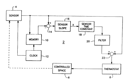
A compensation circuit for sensor lag uses a sensor
temperature signal modification circuit to provide a
modified sensor temperature signal for subsequent use in
controlling the sensed temperature. The compensation
circuit digitally compares a current sensor temperature
representative signal and a sensor temperature signal at a
last or preceeding sample time to produce a difference
signal which is converted to a sensor slope signal and is
multiplied by a sensor time constant. The resulting signal
is passed through a filter to eliminate transient effects
and is summed with the original sensor temperature signal to
provide a sensed temperature signal for control of the
temperature whereby the sensed temperature is a better
estimate of the actual environmental temperature controlled
by a thermostat utilizing the sensed temperature signal.


French Abstract

Circuit de compensation de retard de détecteur, utilisant un circuit de modification de signal de température de détecteur afin de produire un signal modifié qui servira à régler la température détectée. Le circuit de compensation compare numériquement un signal indiquant la température d'un détecteur à un moment donné et un signal indiquant la température du détecteur au temps d'échantillonnage le plus récent ou précédent afin de produire un signal différentiel qui est converti en un signal de pente de détecteur et multiplié par une constante de temps du détecteur. Le signal ainsi produit est filtré afin d'éliminer les phénomènes transitoires puis additionné au premier signal de température de détecteur pour produire un signal de température détectée qui servira à régler la température, la température détectée offrant une meilleure estimation de la température ambiante réelle réglée par un thermostat.

Claims

Note: Claims are shown in the official language in which they were submitted.


- 7 -
The embodiments of the present invention in which an
exclusive property or privilege is claimed are defined as
follows:

1. A compensation circuit for a sensor lag of a sensor
responsive to an environmental condition comprising
means for storing a prior output of a sensor,
means for comparing a present sensor output with the
stored prior output to produce a difference output,
means for converting the difference output to a sensor
slope,
means for multiplying the sensor slope by a
predetermined sensor time constant,
filter means having a fixed time constant for filtering
an output from said means for multiplying and
summing means for adding an output from said filter
means to the present sensor output to produce a control
signal for controlling the environmental condition.

2. A circuit as set forth in claim 1 wherein said means
for storing includes a memory and a clock for timing the
operation of said memory.


- 8 -
3. A circuit as set forth in claim 1 wherein said
condition is temperature.

4. A circuit as set forth in claim 1 wherein said
filter means includes a microprocessor programmed to produce
an output according to:
output = (new value-old value) (1-e- time step/time constant)
+ old value.

Description

Note: Descriptions are shown in the official language in which they were submitted.


2C)1~0~54


BACRGROUND OF THE INVENTION
1. Field of the Invention
The present invention relates to environmental condition
controls. More specifically, the present invention is
directed to apparatus for compensating sensor lag in an
environmental condition sensor to reduce undershoot and
overshoot in an environmental condition control system.
2. Description of the Prior Art
During recovery from an offset environmental condition,
e.g., a sensed environmental temperature is different from a
desired or setpoint temperature, the temperature of the
space being controlled conventionally overshoots the
setpoint temperature significantly more than the temperature
response of the temperature sensor utilized by a temperature
control thermostat. The overshoot effect is a result of the
sensor time constant or lag. The amount of deviation
between the space temperature and the sensor temperature
during a recovery or modification of the temperature to
achieve the setpoint level is approximately equal to the
sensor slope, i.e., ~temperature change) x (the time
constant o~ the sensor). For example, if the temperature
change or ramp rate of the thermostat setpoint i~ 5~F/hr.
then the deviation would be five x .25 hr or 1.25F.
Accordingly, if the sensor reading is 71~F then the actual
environmental would be 71 + 1.25 or 72.25. With a ramp rate


- . "' . ~

.

Z ~ Q 0 ~ 5 ~


of the thermostat of 10~F/hr, the deviation would be 2.5~F
The end result is that to ensure that there will be a
minimum amount of overshoot requires that the ramp rate of
the thermostat must be limited to approximately 5~F/hr
Accordingly, it would be desirable to provide a compensation
circuit for compensating for the deviation of the sensor
temperature from the space temperature during a temperature
recovery by the thermostat.
SUMMARY OF THE INV~;N1ION
In accomplishing this and other objects, there has been
provided, in accordance with the present invention, a
compensation circuit for a sensor lag of a ~ensor responsive
to àn environmental condition utilizing a comparison between
the current sensor output and the last sensor output with a
resulting digital output being converted to a sensor slope
and multiplied by a sensor time constant. The result is
passed through a filter and is added to the current sensor
output to provide a sensed environmental condition signal
for use in controlling the environmental condition.
BRIEF DESCRIPTION OF THE DRAWING
A better understanding of the present invention may be
had when the following detailed description is read in
connection with the accompanying drawing, in which the
single figure is a block diagram of a compensation circuit
embodying the present invention.


. . , ~

2()0~54

_ 4 _


DESCRIPTION OF THE PREFERRED EMBODIMENT
Referring to the single figure drawing in more detail,
there is shown a compensation circuit 2 for a sensor 4 used
for sensing a condition, e.g., temperature, of a controlled
space or environment 6. ~he temperature of the controlled
space 6 is controlled by means of a thermostat 8 which is
provided with an output from the compensation circuit 2 to
effect such a control. The sensor 4 includes an
analog-to-digital (A/D) converter to convert the sensor
output which may be in the form of a variable resistance to
a digital number that corresponds to the sensed temperature
of the controlled space 6. The sensor 4 may be incorporated
in the thermostat 8 as part of a common housing. The value
of the ~ensed temperature at the time that the last
conversion by the sensor 4 was made is stored in a memory
10. The memory 10 and the analog-to-digital conversion
operation by the sensor 4 are controlled by a clock 1~. The
memory 10 and the clock 12 may be part o~ a microprocessor
also incorporated in a common housing with the thermostat
8. A typlcal time step for the A/D conversion operation may
be one minute.
The ou~put from the memory is periodically applied to a
f irst summing node 14 as a digital word representative of
the sensor temperature at the last time step whereby the
difference between the current sensed temperature from the


..' ' ' ~
. .
- : . . . . . . .

~O ~ U ~ 5 4


sensor 4 and the previous sensed temperature is summed at
the node 14 and the node output applied to a sensor slope
derivation 16. The sensor slope is determined by dividing
the node output, i.e., the temperature difference, by the
time step to give a slope, e.g., ~F/hr. The sensor slope 16
may be also part of the aforesaid microprocessor whereby a
stored program may be used to effect the sensor slope
computation. The sensor slope is subsequently multiplied by
- a sensor time constant 18 which i~ a stored value obtained
by a prior performance testing of the sensor, e.g., 15
minute3. Subsequently, the output of the sensor time
constant 18 is applied through a filter 20 having a fixed
time con~tant, e.g., a digital equivalent of an electronic
filter whereby the aforesaid microprocessor computes the
output of the filter 20 according to the relationship of
output - new value - old value x (l-e~ time step/time
con9tant) + old value. Thls enables the compensation
circuit to neglect transients in the signal.
Finally, the output of the filter 20 is combined with
the current sensor temperature signal at a second summing
node 22 and the resulting output is applied to the
thermostat 8 as a control -cignal for the thermostat 8 in
controlling the temperature of the controlled space 6 The
aforesaid filter equation is solved at each time step to
provlde an output signal for the thermostat 8 at each time


, - . . -

- zo~s~


step. During normal operation, the sensed temperature stays
fairly constant so the slope is substantially zero whereby
no compensation is needed since sensed temperature equals
actual temperature. During an extended ramping period
wherein the thermostat is attempting to bring the
temperature of the controlled space to match a setpoint
temperature, the sensed temperature would lag the actual
temperature in an amount proportional to the thermal time
constant of the sensor.
The compensation circuit of the present invention
provides a means for compensating for the deviation of the
sensed temperature from the controlled space desired
temperature during the recovery by the thermostat 8. In
; effect, the sensor temperature is made equal to the desired
temperature. As a result, it is possible to go to a higher
ramp rate for the thermostat and obtain greater energy
savings while still minimizing overshoot or undershoot.
Thus, the compensation circuit provides autcmatic
compensation during extended ramping such as a recovery
after night's setback of the thermostat. It should be noted
that the compensation of the present invention is equally
effective for cooling mode of operation as well as heating.
Accordlngly, it may be seen that there has been
presented, in accordance with the present invention, a
compensation circuit for minimizing overshoot and undershoot
of an environmental condition control system.


.: -
,
' ' . - ' ' ~ ' '
~: ' : ' - ' .. ' '

Representative Drawing
A single figure which represents the drawing illustrating the invention.
Administrative Status

For a clearer understanding of the status of the application/patent presented on this page, the site Disclaimer , as well as the definitions for Patent , Administrative Status , Maintenance Fee  and Payment History  should be consulted.

Administrative Status

Title Date
Forecasted Issue Date 1997-12-23
(22) Filed 1989-10-17
(41) Open to Public Inspection 1990-06-14
Examination Requested 1996-02-08
(45) Issued 1997-12-23
Deemed Expired 2006-10-17

Abandonment History

There is no abandonment history.

Payment History

Fee Type Anniversary Year Due Date Amount Paid Paid Date
Application Fee $0.00 1989-10-17
Registration of a document - section 124 $0.00 1990-02-26
Maintenance Fee - Application - New Act 2 1991-10-17 $100.00 1991-09-27
Maintenance Fee - Application - New Act 3 1992-10-19 $100.00 1992-09-28
Maintenance Fee - Application - New Act 4 1993-10-18 $100.00 1993-09-27
Maintenance Fee - Application - New Act 5 1994-10-17 $150.00 1994-09-22
Maintenance Fee - Application - New Act 6 1995-10-17 $150.00 1995-09-20
Maintenance Fee - Application - New Act 7 1996-10-17 $150.00 1996-09-20
Final Fee $300.00 1997-07-07
Maintenance Fee - Application - New Act 8 1997-10-17 $150.00 1997-10-01
Maintenance Fee - Patent - New Act 9 1998-10-19 $150.00 1998-09-30
Maintenance Fee - Patent - New Act 10 1999-10-18 $200.00 1999-10-04
Maintenance Fee - Patent - New Act 11 2000-10-17 $200.00 2000-09-20
Maintenance Fee - Patent - New Act 12 2001-10-17 $200.00 2001-09-19
Maintenance Fee - Patent - New Act 13 2002-10-17 $200.00 2002-09-18
Maintenance Fee - Patent - New Act 14 2003-10-17 $200.00 2003-09-17
Maintenance Fee - Patent - New Act 15 2004-10-18 $450.00 2004-09-16
Owners on Record

Note: Records showing the ownership history in alphabetical order.

Current Owners on Record
HONEYWELL INC.
Past Owners on Record
BECKEY, THOMAS J.
Past Owners that do not appear in the "Owners on Record" listing will appear in other documentation within the application.
Documents

To view selected files, please enter reCAPTCHA code :


To view images, click a link in the Document Description column. To download the documents, select one or more checkboxes in the first column and then click the "Download Selected in PDF format (Zip Archive)" or the "Download Selected as Single PDF" button.

List of published and non-published patent-specific documents on the CPD .

If you have any difficulty accessing content, you can call the Client Service Centre at 1-866-997-1936 or send them an e-mail at CIPO Client Service Centre.


Document
Description 
Date
(yyyy-mm-dd) 
Number of pages   Size of Image (KB) 
Cover Page 1994-03-26 1 17
Cover Page 1997-12-11 2 61
Abstract 1994-03-26 1 31
Claims 1994-03-26 2 40
Drawings 1994-03-26 1 18
Description 1994-03-26 5 187
Representative Drawing 1997-12-11 1 7
Prosecution Correspondence 1996-02-08 1 38
PCT Correspondence 1997-07-07 1 29
Prosecution Correspondence 1996-03-18 1 39
Office Letter 1996-02-29 1 49
Prosecution Correspondence 1996-02-29 1 42
Fees 1996-09-20 1 72
Fees 1995-09-20 1 78
Fees 1994-09-22 1 74
Fees 1993-09-27 1 59
Fees 1992-09-28 1 54
Fees 1991-09-27 1 33