Note: Descriptions are shown in the official language in which they were submitted.
2000956
MULTIPL~ CHANNEL DATA ACOUISITION ~YSTEN
The invention pertains generally to systems for the
acquisition of analog data by digital processors and is
more particularly directed to such systems which include
many high speed data acquisition channels.
The acquisition of analog data by a digital processor
is known to include the conversion of an analog signal to
a digital form by an analog to digital converter and the
input of the converted digital value by the processor over
0 a data bus. The data in digital form, once stored in the
processor memory, can be further processed and used for a
variety of purposes. Software process control systems
based upon the digital conversion and input of sensed
analog values are common. Other systems use converted
analog data for diagnostic purposes where the values
pertain ~o limits or alarm values. Another of the more
advantageous uses for such systems is to collect data
relating to a physical event from a multiplicity of the
sensors for later analysis.
Systems for the collection of physical data and its
digitization and storage are prevalent in scientific
systems where vast quantities of data need to be analyzed.
Examples of such disciplines where these systems have been
used to advantage are physics, astronomy, medicine,
chemistry and others. Physical event data acquisition
systems generally present the problem of simultaneously
digitizing many data channels and efficiently recording the
outputs of the channels from which the individual data was
taken.
A specific example of an advantageous use of this type
of data acquisition system would be in connection with a
barrel-shaped electromagnetic calorimeter termed the High-
Density Projection Chamber (HPC). The HPC is a fine
grained gas sampling calorimeter which uses the principle
of time projection to obtain a three-dimensional
localization of the energy deposition within it. A series
of proportional tubes with U-shaped cross sections are used
to amplify the drifted charge and the signals induced on
- - ,
; -
,
" 2000956
2 --
the cathodes of these tubes are collected on a series of
pads. The HPC includes 128 readout pads in each of 144
sectors, for a total of 18,432 readout channels.
This calorimeter can be utilized to measure the charge
deposited by photons, electrons or other charged particles
passing through it. An interesting physical experiment in
which charged particles are generated for basic elementary
particle research will be performed at the ~arge Electron
Positron Collider, in which two charged particle beams are
0 collided to radiate a number of other smaller charged
particles. These emitted particles can then be detected by
measuring the energy which they impart to the gases of the
barrel calorimeter upon impingement.
However, in order to resolve the energy of single
photons and pions, the calorimeter in such instances would
have to sample the collected charge 256 times per event
over the 90 cm. drift length of each calorimeter sector.
This necessitates the collection of digitized charge
information for approximately 4.7 X 10⁶ spatial samples per
event. Moreover, the beam crossing rate of the collider
requires that digitization of the charge deposited by the
particles traversing the calorimeter occur at a frequency
of about 15 MHz. Additionally, the charge deposited by
individual pions and electrons is relatively small with
respect to groups or showers of particles. In order to
provide for the sampling of minimum ionizing particles and
showers of energies > 20 GeV without appreciable
saturation, a dynamic range of approximately aoo: 1 is
needed. Therefore, the data acquisition system for such
configuration must convert massive amounts of analog
information to a digital format in a very short time and
over a large dynamic range.
In scientific digitization systems generally, and
particularly in the HPC example, there is much of the time
no relevant data present in many of the data samples. Such
digitizations of irrelevant values, or even zero values,
take up memory space and they should be discarded.
However, the time constraints of data acquisition for a
- . - ~, ,. : . . . . .
.
:. : : .
Z0~956
_ 3 _
large number of channels for such systems make such further
data processing difficult to accomplish concurrently.
The calibration of data acquisition systems with a
large number of data channels further presents difficulty.
The gains and zero values for each channel must be set
before the digitization system can take an accurate
measurement. With a large number of data channels a manual
calibration, or even an automated calibration, can take a
significant amount of time.
0 Another difficulty encountered with the digitization
of data from a large number of data channels is the
efficient transfer of the data from the acquisition system
to a host processor. When massive amounts of data must be
moved from one system to another, an efficient
communications interface must be used. Otherwise, the
acquisition system will spend more time transferring the
data than acquiring it. A method of providing efficient
data transfer for digital systems is to make the transfer
hierarchial where data can be preprocessed before transfer
to the host. Preprocessing can further be accelerated by
distributing the processing engines, either serially or in
parallel. An efficient communications interface which can
be used to connect a host processor with a large number of
peripheral devices is the FASTBUS. This bus, which
implements IEEE Standard 960-1986 for communications, is a
32-bit wide gateway for data and information between a host
and its peripherals. However, this efficient
communications interface has not been used in a data
acquisition system utilizing a distributed and/or
hierarchial preprocessing data transfer technique.
5ummary o~ the Invention
The invention solves these and other problems of data
acquisition systems by providing a system which efficiently
digitizes information from a multiplicity of channels and
transfers it to a host processor.
In a preferred embodiment, a data acquisition system
includes a plurality of data acquisition modules, each
adapted to digitize the analog information from a
.~,.
,~,.. .
2q)~ 956
- 4 -
: '
multiplicity of input channels. Each module includes a
communications coupler which interfaces with an efficient
communications structure for transferring data to a host
processor. In the implementation illustrated, the
communications coupler connects each module to a FASTBUS
backplane which is then interfaced to the host processor.
Each data acquisition module comprises, in addition to
the communications coupler, a multiplicity of input
digitization circuits including a flash analog to digital
converter (FADC), a cache memory for buffering converted
information, and means for reading data from said cache
circuit onto a submodule bus. The modules are triggered by
the host to convert a plurality of sequential time slots
(event) into digital samples which are then stored to the
cache memories.
Each submodule bus connects the cache memories of a
plurality of the input channels to a front end buffer
(FEB). Between the FEB and each cache is a zero
suppression circuit which filters the data for non-zero
values. Because only non-zero values of the data are
passed from each cache memory to a FEB, each FEB is divided
into two sections where one section stores the data samples -
and another section stores a digital value corresponding to
a time slot at which the data was taken.
The zero suppression circuit, including an address
generator, will reject data values based on a threshold
amplitude and a threshold duration or width. The data
values are clocked sequentially out of each cache memory
and the address generator determines whether the data is
retained or not. The selection is made by first clocking
the data into the FEB at an address generated by the
address generator and then retaining the data by
incrementing the address or discarding the data by
overwriting depending on whether it passes the zero
suppression criteria. The zero suppression criteria, in
the preferred implementation, threshold and width, are
stored in a random access memory which can be read and
written to change the parameters stored therein.
. . - ............. ~. . .. ..
- . : .: . : . . ~ : ~ : .
: .
Z0~)0956
In the preferred embodiment, zero suppression is
effected if a data sample does not exceed a threshold,
which in turn exceeds a pedestal level. The pedestal
levels are determined from the zero values of each FADC of
the module during a calibration operation. If the data
sample is above the threshold, it will be tentatively
stored until it is determined if the subsequent two samples
are above the threshold thereby passing the width test.
The FEB is further partitioned into individual memory
o spaces for each associated channel which can hold multiple
events for that channel. The partitioning is such that
each event begins at a fixed location in the FEB. The
lower order byte at this location contains the valid word
count for the channel, i.e., the number of data words
corresponding to non-zero data values.
Each module further comprises a module bus and a local
processor with random access memory which is further
connected to the module bus. The module bus exists as a
pathway between the FEB of each submodule, the local
processor, the module event buffer memory, threshold and
width memories, and the communications coupler. The FEB,
threshold and width memories, and the module event buffer
exist in the memory space of both the local processor and
the communications host.
25- This architecture provides an advantageous method for
transferring digitized data to the communications host. In
a first method, the communications host can directly access
and upload from the FEB of each submodule of each module.
Alternatively, the local microprocessor can upload the data
from each submodule to the event buffer and the
communications host can upload each event buffer from each
module.
This method is advantageous in that the local
processors of each module work in parallel to process the
data from the FEBs to a single place in each module event
buffer where more effective block transfers of data are
possible. The local processor also works in series with
the zero suppression processor to provide a hierarchial
200(:~956
- 6 -
processing technique. In addition, the local processor is
capable of reformatting the data from FEB format to a
format compatible with the communications host. Moreover,
the system with the local processor is capable of
additional data compression and analysis or other front end
processing on the FEB data. The amount of processing by
the local processor is variable to the degree needed for a
particular application. Any number of different proqrams
can be provided, since the local processor program is
downloaded into the module memory before the beginning of
data collection.
According to another feature of the invention, each
local processor can auto-calibrate the FADC channels
associated with its module. The local processor performs
the calibration by executing a calibration program
downloaded from the communications host. The calibration
program disables the zero suppression and averages a number
of data samples taken during a quiescent event time of the
input device. From these samples the local processor
computes a pedestal level for each channel under its
control. Since all the local processors operate in
parallel, a calibration which otherwise would be laborious
and time consuming can be accomplished with facility.
These and other objects, features, and aspects of the
invention will become apparent and more fully described
upon reading the following detailed description when taken
in conjunction with the attached drawings wherein:
Brief Description of the Drawings
FIG. 1 is a system block diagram of an apparatus for
measuring a physical event incorporating a data acquisition
system constructed in accordance with the invention;
FIG. 2 is a detailed block diagram of one of the
segments of the event generator illustrated in FIG. 1
showing the module groupings associated therewith;
FIG. 3 is a detailed functional diagram of one of the
data acquisition modules of the data acquisition system
illustrated in FIGs. 1 and 2;
. : -
~. .. . .
., , , , . - . . .
:
.. . . . . - ..
- :, . . ~ .. ,
2Q009~;6
- 7 -
FIG. 4 is a detailed hardware block diagram of the
module bus, local processor, the FASTBUS coupler, and their
interconnections;
FIG. 5 is a detailed block diagram of the timing and
5control circuitry associated with the module illustrated in
FIG. 3;
FIG. 6 is a pictorial representation of various timing
and clock signals generated by the circuitry illustrated in
FIG. 5;
loFIG. 6A is a schematic of the watch dog driver of the
system;
FIG. 7 is a detailed electrical schematic of the input
channel circuitry illustrated in FIG. 3;
FIG. 8 is a detailed electrical schematic diagram of
15the circuitry to generate the plurality of reference
voltages which are used by the FADC illustrated in FIG. 7;
FIG. 9 is a detailed electrical schematic diagram of
the FEB of one submodule illustrated in FIG. 3;
FIG. 10 is a pictorial representation of the
20allocation of memory space in a FEB of one submodule
illustrated in FIG. 3;
FIG. 11 is a pictorial representative of the
allocation of memory space for the threshold and width
memories of the module illustrated in FIG. 3;
25FIG. 12 is a detailed electrical schematic diagram of
the controi circuitry for the FEB memory and the threshold
and width memories of the module illustrated in FIG. 3;
FIG. 13 is an electrical schematic diagram of the
threshold and width memories, and address generators which
30form the zero-suppression circuitry of the module
illustrated in FIG. 3;
FIG. 14 is a detailed electrical schematic diagram of
one of the address generators illustrated in FIG. 13;
FIG. 15 is a pictorial representation of various data
35samples being compared by the zero suppression circuitry;
FIG. 16 is a detailed electrical schematic of the
local processor, control interface, arbitration logic,
control status register, and interrupt control illustrated
' : '~ <
:-
" ' ~ .
' ' - . .:'' , . :
2000956
-- 8
in FIG. 4;
FIG. 17 is a detailed electrical schematic of the
module memory, cross connect, and memory control
illustrated in FIG. 4;
FIG. 18 is a detailed block diagram of the FASTBUS
coupler illustrated in FIG. 4;
FIG. 19 is a pictorial representation of timing
waveforms representing a communication between the FASTBUS
backplane and the FASTBUS coupler illustrated in FIG. 18;
FIG. 20 is a system flow chart of the executive
program for controlling the data acquisition system
illustrated in FIG. l; :
FIG. 21 is a detailed flow chart of the initialization
routine illustrated in FIG. 20;
FIG. 22 is a detailed system flow chart of a threshold
calibration operation;
FIG. 23 is a detailed system flow chart of a gain
computation operation; and
FIG. 24 is a pictorial representation of a reformatted -
data blocklet sent to the host by the local processor.
.. ' ~ .. ' .: , .
:
'. , ~ '' " '
- . .
. ~ . . .
.
2000956
g
Detailed De~cription of the ~Preferred Embodiment
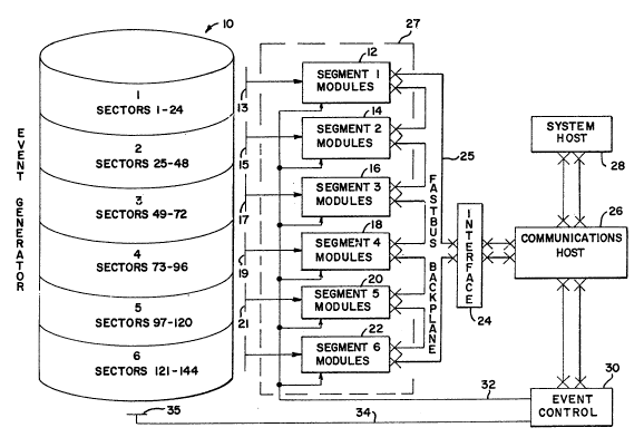
FIG. 1 illustrates a system for the acquisition of
digital data related to a particular physical event which
includes a data acquisition system constructed in
accordance with the invention. The system includes an
event generator 10 which is a device equipped with a
multiplicity of sensors to take measurements of a physical
phenomena. As an example, the specification will use as
an event generator the barrel calorimeter described for the
0 HPC. While data acquisition for this particular phenomena
requires a multiplicity of data sensors, there are many
other event generators which are equivalent in that they
require many sensors operating simultaneously to record an
event properly.
In the system illustrated in FIG. 1, the event
generator 10 comprises six segments 1-6, each having 24
sectors, for a total of 144 sectors. Each sector 1-144 has
multiple data sensors shown schematically at 13, 15, 17,
19, 21 and 23 which connect to groups of segment
modules 12, 14, 16, 18, 20 and 22, respectively. The
segment modules contain a plurality of modules for each
sector and segment, such that sufficient circuitry is
provided to digitize all the analog signals detected by the
sensors. The segment modules 12-22 connect to a
communications bus 25 which transfers the recorded digital
data from the sensing of an event to a communications
host 26 through an interface 24. In the preferred
embodiment, this communications bus 25 is a master/slave
driven communications interface termed a FASTBUS. The
segment modules 12-22 are identical such that they
interconnect easily to the FASTBUS backplane 25.
The communications host 26 is under a control of a
system host 28 to input and process the data which is
measured by the data acquisition system 27. The system
host 28 communicates to the data acquisition system 27 via
the communications host 26 and the interface 24. An event
control 30 further communicates to the system host 28
through communications host 26. The event control 30
. .
, ,
- ~
Z000956
- 10 --
provides timing and clock lines 32 to the segment
modules 12-22. The event control 30 further has sensors 35
which are read on lines 34 which do not take data but are
for event control and processing of the data acquired
during an event.
In operation, the sensors 35 attached to sensor
lines 34 detect particular parameters and cues concerning
the physical status of the event generator 10 and cause the
event control 30 to issue a trigger to begin the data
acquisition by data acquisition system 25. The data
acquisition system 25 digitizes the inputs from the
multiplicity of sensors 13-23 and then transfers this
acquired data either in full or compressed form via the
FASTBUS backplane 25 to the communications host 26 and
eventually the system host 28.
If, during the digitization, the event control 30
determines that the detected event is not interesting, then
it can reset the data acquisition system 27. Thus, the
system will only digitize during events (triggers) and only
for the amount of time necessary to determine the event may
have significant data. If there is a determination that
the data is interesting then it will be stored and further
processed. The segment modules 12-22 will communicate to
the communications host 26 whether significant data is
stored or not.
A more expanded view of the modules which comprise one
segment group, for example segment group 12, is shown in
FIG. 2. Each segment module group contains 24 sector
groups of which sector 1 at 40 is an example. Sectors 2-
24 are represented as sector modules 50-62, respectively
and contain the same configuration and number of modules
that sector 1 at 40 contains. The sector 1 group comprises
four modules 42, 44, 46 and 48, each of which are coupled
to the FASTBUS backplane 25 and to a plurality of sensors
39 for the respective sector of a segment. In a preferred
embodiment, each module, for example 42, digitizes the
inputs from thirty-two channels 0-31. The total system,
thus, instruments 128 channels for each of the 144 sector
- . . . .
' . . ' ,, ~
` 2000956
-- 11 --
groups for a total of 18,432 channels. Because of the
particular event generator 10 described, 256 time slots are
measured per event. Total digitized information for the
system of approximately 4.7 x 10⁶ data words- are thereby
recorded per event. Such massive data acquisition in a
relatively short period of time requires the efficient and
extremely fast data acquisition system which is provided by
the invention.
With respect now to FIG. 3, there is shown a detailed
lo block diagram of one module, for example the one designated
42 in FIG.2, of the multi-channel data acquisition systèm.
The module 42 comprises a plurality of submodules 66, 68,
70, and 72 connected to a module bus 77. Each of the
submodules, for example 66, includes a plurality of input
channel circuits comprising an input channel group (for
example, channel group 80) a zero suppression circuit 82,
a FEB (FEB) 84, and gates 86, 88. Each of the input
channel circuits of a channel group 80 includes an input
amplifier 92, a flash analog to digital converter (FADC)
94, a cache memory 96 and a gate 98.
The module further includes a local processor 104
connected to the module bus 77 and associated module memory
106 similarly connected to the module 102 bus. Completing
the elements of the module 42 is a communications coupler
102 coupling the module bus 77 to the FASTBUS backplane 25.
In operation, the analog signal from the respective
event sensor is input to the amplifier 92, differentially
amplified, and then converted to a digital value by FADC 24
at a specified clock rate. The digital values are
temporarily stored in the cache memory 96 of the input
channel circuit until an entire event is recorded
(256 samples). When the loading cycle is complete, the
data is transferred (dumped) to the FEB 84 from each cache
memory of the eight channels in the group. The unloading
of the cache memories for a group 80 is sequential, with
the first finishing before the next starts. Gate 86 which
is closed for the load cycle is open during the dump cycle
,
.. . : , . .
., . : . . : . ..
201)0956
- 12 -
and is connected to the open gate of group 80 in sequence.
The data flows first to the zero suppression circuit 82
which causes data values below a threshold and less than a
predetermined width to be discarded.
5After data from the cache memories of the associated
channel groups have been transferred to the FEBs of the
submodules 66, 68, 70 and 72, one of two operations may
take place to upload the data to the communications host
26. The first operation includes the direct addressing of
0the FEBs by the communications host 26 to take the
information directly. The communications host 26
accomplishes the transfer by enabling gate 88 of a
submodule, and by then addressing the FEB 84 directly.
Alternatively, and more advantageously, the local processor
15104 controls the transfer the information stored in each
FEB for each submodule into the section of module memory
106 designated as the module event buffer 100. The
communications host 26 can the perform a block transfer of
all the data for a module by addressing the module event
20buffer 100. The local processor 104 is halted during the
load and dump cycles of the submodules so that it will not
interfere with the sensitive analog sensors of the design.
In the preferred implementation shown in the drawing,
the module 42 is capable of digitizing 32 channels of
25information, CHAN0-31. These 32 channels are partitioned
into groups of 8 input channel circuits, where each group
shares a zero suppression circuit and a FEB. While each
group shares a zero suppression circuit, there is provision
for each input channel to have its own suppression
30criteria. A group of 8 input channels, a zero suppression
circuit and a FEB form one of the four submodules. The
four submodules, the module event memory 106, the local
processor 104, the module bus 77 and the communications
coupler 102 comprise the module 42.
35A more detailed block diagram of the local processor
104 and the module bus 77 are shown to advantage in
Figure 4. The module bus 77 comprises a control bus 108,
a 19-bit wide address bus 110, and a 3~-bit wide
:
: `' '
:
.: : . - .. .. , . -. ... .
. . . ~ . . . .
;~:000956
bidirectional data bus having data lines D0-D15 and data
lines D16-D31 at 112. The module bus 77 is common to the
local processor 104j the communications coupler 102 and the
module memory 106 thereby allowing access of the module
memory by either the local processor or the communications
host through the coupler 102.-
The system further includes arbitration logic 114 to
determine which processor, the local processor 104 or host
processor, will control the bus 77, for how long and by
what protocol. A control interface 56 also generates
control signals which assist the local processor and the
communications coupler to handle the module bus 77. In
addition, the control interface provides control signals to
a cross-connect circuit 60 to allow the data on line D0-D15
of the data bus to be applied to the opposite data lines
D15-D31, and vice versa. A control status register CS10 at
118 is selected by control lines from the address bus 110
to select the module. Once selected, the control status
register CSR10 inputs data from the communications coupler
via the data bus 112. These data are the control commands
of the communications host for the local processor 104.
The commands of the control status register 118 are
translated by an interrupt control 120 into interrupts
which command a microprocessor 122 to transfer command
processing to selected control routines. The memory
control 124 is accessible by both the local processor 104
and the communications host 26 to either read or write data
into the module memory 106.
Because the communications coupler 102 uses a 32-bit
data bus and the microprocessor 122 uses a 16-bit data bus,
it is necessary to reconfigure the data bus 112 dynamically
from 32 to 16 bits. This is done by a cross-connect
circuit 128 which connects data lines D16-D31 to their
corresponding data lines D0-D15 when the microprocessor 122
tries to access data that would be in the upper 16 bits in
a 32-bit word. The control signals provided by the
communications coupler 102 are not the same as those
recognized by the microprocessor 122 and module memory 106.
.
. : ~ , : ~,, : : :. , :~
200(1956
- 14 -
Therefore, control interface circuitry 126 is provided to
transform the signals from the FASTBUS coupler 102 into
compatible signals.
The system has a series of triggers or levels which
causes data from individual events to be accepted for
further processing or discarded as not of current interest.
These trigger levels provide a prefilter or preprocessor
for the massive amounts of data which the system is able to
digitize. The system is presently configured to be capable
of digitizing 18,432 sensor output channels, each having
256 samples, every 22 microseconds. If all of this data
were stored even for a short time, the processing
capabilities and storage of the host would be overextended.
Because in many physical experiments much of the data is
not interesting, as it does not include the event being
searched for, extraneous values should be discarded at the
earliest possible time in the system processing cycle so as
not to tie up higher level system assets.
Therefore, at a first level, the system is triggered
to begin taking data for an event. In the present example,
this trigger is coincident with the beam crossing of two
particle beams which produces charges in the calorimeter.
No trigger is applied to the system unless there is a good
possibility that significant data will result, i.e., a
prescreened event occurs. If during the digitization of an
event or the buffering of the data in the FEBs, the event
control 30 decides that the event data should not be
further processed, then a second level trigger will reset
the system. The transfer of the digitized data will not be
made, but the system will instead cycle back to an idle
mode and be immediately ready to digiti~e another event
upon synchronization with the next beam crossing. With
this priority triggering system, only a few events out of
the many possible will be digitized by the first level
trigger, for example, l event in 100 possible events.
Still fewer, those which after digitization were noted to
be of interest will be- stored to the FEBs, for example, 1
event in 100 of those digitized. Of the events which are
.-: .... .. : . . :
. - ~ . :
: .:: .
. .
2~0~956
stored in the FEBs, the data therein has also been
effectively compacted by zero suppression.
A third level of triggering is provided by the local
processor 104. The local processor by means of various
S computations, or other system functions, can preprocess the
data stored in the module event buffer to determine if it
contains information which may require further processing.
In this case the module will signal the communications host
it has data ready. If the information the data contains
has been totally zero suppressed or otherwise discounted,
the module will not signal the host. Further, during the
transfer of the data from the FEBs to the module event
buffer, the data can be further compressed by the
clustering program.
The hierarchial triggering procedure produces a system
whereby only highly compressed data packets which are known
to contain relevant information are transferred to the host
for final analysis. The preprocessing or data screening
occurs at every step of the data flow to eliminate
irrelevant data and to compact that data which is relevant.
Further, the preprocessing steps become more intelligent
and more complex as more is known about the entire overall
event and data samples.
Fig. 5 illustrates the detailed circuitry of the
timing control of the data acquisition system illustrated
in Figs. 1-4. In general, there are a number of basic
system timing signals which are operated on logically by
the circuitry to produce timing and enabling signals which
convert the channel voltages to digital numbers, store
those digital numbers in the cache memories, unload the
cache memories to the FEBs, and provide system control of
this process.
The analog to digital conversion process is controlled
overall by two R-S bistables 200 to 202 and a binary/Grey
counter 204. The bi$table 200 is set by a signal W/C after
being shaped in inverter 202. The W/C signal is the
warning/clear signal which alerts the system that an event
which is to be sampled is about to begin. This signal,
~, .: - . ,, ` ': . ' :.
' - : :: ' , :
2~00956
- 16 -
therefore, sets the bistable 202 to produce the signal LOAD
at the Q output of the device. When the load cycle for the
cache memories is complete, the bistable 200 will be reset
by the signal load end, LDEND. The time between the
warning/clear signal W/C and the load end signal, LDEND, is
20 microseconds. After the load cycle the bistable 202 is
set to generate at its Q output a signal DUMP which unloads
the caches into the FEBs. The bistable 202 is set by the
signal LDEND which indicates the end of the load cycle and
0 the beginning of the dump cycle. When the dump cycle is
complete, the bistable 202 is reset by the signal DMPRST
which is applied to its reset input, R. The dump cycle is
455 microseconds in duration. Both bistable 200 and 202
are cleared by the RESET signal applied to their respective
clock inputs CK. The signal RESET will produce a clearing
of both bistables such that a new warning/clear signal can
restart the load/dump cycle immediately. This is a second
level trigger which rejects the data presently being loaded
into the system.
The counter 204 is a binary/Grey counter which has
binary outputs B0-B7 and a Grey code outputs, CA0-CA7. The
counter 204 has the address outputs CA0-CA7 connected to
the address lines of the cache memories so that all receive
a Grey code address output which only changes one bit for
each address increment. In this manner, the cache memories
may be loaded very quickly from the FADCs without address
mistakes due to noise and settling times. Binary addresses
from outputs B0-B7 are used to store the time slots for
particular data values that are stored in the cache
memories. The cache memories are loaded in parallel and
thus the address output CA0-CA7 are stepped through once
from 0-255. Thereafter, the cache memories are unloaded
into the FEB and address outputs B0-B7 are incremented from
0-255 eight times.
The input SUB of the counter is connected to the
logical *Q output of a D-type bistable 206. This output
adjusts the cache memory address to align with the FEB
address. The clock input CLK of the counter receives a
- - . . . . .
.
::
21)0~956
- 17 -
signal SUBCL~ which changes depending upon whether the
counter is providing addresses for the load cycle or the
dump cycle. During the load cycle, the counter 204 is
counted at a fast rate of 14.675 MHz by a clock which input
through NAND gate 208 and 210. NAND gate 210 is configured
as a negative true input OR gate which serves to pass one
of three signals from NAND gates 208, 212, or 224. The
high speed or fast clock in enabled to the counter 204 via
NAND gate 208 provided it is coincident with a flash enable
signal, FLEN. The flash enable signal is output from NAND
gate 216 which passes the beam crossing signal, BCO, from
shaping inverter 218 provided the load cycle has not ended,
as determined by the LDEND signal, and the system is not
reset, as determined by the *RESET signal. OR gate 220
causes the FLEN signal to become latched on the rising edge
of the BCO signal until either the load end signal or
*reset signal occur. Prior to the BCO signal however, a
pre-sample window signal PSW can enable the 14.675 MHz
clock through NAND gate 212. The PSW signal is applied
through shaping inverter 222.
During the dump cycle, a slower clock, a 4.5 MHz
signal, is input through a shaping inverter 226. The
signal is gated to the NAND gate 210 by applying the DUMP
signal to one input of NAND gate 224 whose other input is
the 4.5 MHz signal. When the load cycle is completed, the
DUMP signal makes a low to high transition and NAND gate
224 is enabled to allow clock pulses to flow through NAND
gate 210 and clock the counter at the slower rate.
The LOAD and the DUMP signals are further used for
general enabling signals for the input channel circuitry of
the data acquisition system. A buffer 228 and a buffer 230
generate the enabling signals allowing the flash A/D
converters to operate and the cache memories of the input
channel circuitry to be read and written. Buffer 228 is
enabled by grounding its inputs EA and EB. Therefore, the
signals applied to its A0-A3 inputs appear at its YA0-YA3
outputs, and similarly, the inputs which appear at the B0-
B3 inputs will appear at its YB0-YB3 outputs. The LOAD
.
. . . - , . - . : . : . :. .
2~0(~1956
- 18 -
signal is applied in parallel to inputs A0-A3 to become
four flash clock enable signals, FLCE 0-3 at the outputs of
the buffer 228. Similarly, the inverted load signal *LOAD
is applied to the B0-B3 inputs of the buffer. These
signals become the cache write enable signals, CAWE0-3. The
FADCs are supplied with the 14.675 MHz signal by buffer
230. The clock signal is applied to the A0-A3 inputs and
is fanned out to become the flash clock signals, FLC0-3
from the YA0-YA3 outputs, respectively. The cache chip
0 enable signals CACE0-3 from buffer 230 are fan outs of the
CACHE signal from OR gate 232 applied to the B0-B3 inputs
of the buffer. The CACHE signal is a logical combination
of the LOAD signal or the DUMP signal, thus, asserting the
signal during both the load and dump cycle.
The circuitry which provides the reset includes
negative true input OR gate 238. The reset provided by the
system can be one of two types. A long reset LRST which is
applied to OR gate 238 via invertor 236 or the quick reset
QRST applied by the system through shaping invertor 242.
The output of OR gate 238 can either be applied directly to
reset circuitry or inverted by invertor 240 before applying
the reset. The long reset LRST is generated by a timer 234
which is triggered by the output of negative time input OR
gate 232. A number of signals are provided to produce
alternative triggers for the long reset LRST. The first is
a power up reset where a voltage +V is attached to
capacitor 244 through resister 246. When power is applied
to the circuit the input of gate 232 goes low triggering
the timer 234. Similarly a system reset SBR applied by the
module circuitry produces a similar result. A manual reset
is provided by attaching a push button to a grounding line
to generate the signal MRST to gate 232.
The cache busy signal CABUSY is directed to other
circuitry in the module and causes the local processor 104
to halt and denies the host access to the module memory
until the cache busy is done. This produces a noise free
environment for converting and storing the event data
without interference which could cause data errors. The
- . . , : :
,
2~00956
- 19 -
cache busy signal, CA8USY, is provided by the output of
NAND gate 254 which initiates the signal when the LOAD
signal is asserted through OR gate 256 providing the reset
signal *RESET is not asserted. The load signal will cause
the CABUSY signal to be asserted by latching itself through
NAND gate 258 until the dump end signal is present. The
CABUSY signal will be asserted from the beginning of the
LOAD signal until the end of the DUMP signal.
Another signal from the timing circuitry in Fig. 5 is
signal RSA which is generated to reset the FEB circuitry as
either an output from NAND gate 250 or the *RESET signal
applied to one input of OR gate 252. The RSA signal output
from NAND gate 250 is the coincidence of the signals from
the output of NAND gate 246 and the Q output of D-type
bistable 248. The D-type bistable has its D input tied to
the signal line T255 and its clock input to a monostable
244 which is triggered from the TDl output of counter 242.
NAND gate 246 detects the coincidence of the output signals
TD2 and TD3 of counter 242. The counter 242 is clocked by
the dump clock signal DCLK applied to its input IN. In
operation, the circuitry acts to reset the FEBs after eight
dump cycles to produce the storage of different events from
the eight cache memories which are associated with each
FEB.
Fig. 6 illustrates the timing waveforms for the front
end of the data acquisition system illustrated in Fig. 1.
In general, the beam crossing signal BCO or first level
trigger begins a 20 microsecond load cycle. During the 20
microsecond load cycle, the flash clock causes the cache
buffers to be filled with 256 data samples. Because the
sampling is done in parallel the buffers of all modules are
filled simultaneously. During this time the cache busy
signal, CABUSY, is asserted at a high logic level such that
the local processor 104 is halted and no memory transfers
from the host will take place over the module bus. At the
end of the 256 clock cycles (T255) which are necessary to
fill the cache memories, the dump cycle which is 455
microseconds in length begins. This unloads the cache
. . . .
~' . . ' . ' :, : ;: '
, ~, . ~, :
: , , :
,
. . : .. :: : ~ . .. :
2~0~956
- 20 -
memories for each module into one of the multiplexed FEBs.
The cache busy signal CABUSY is continually asserted during
this time period. Any time after the load cycle has been
completed to fill the cache buffers, the quick reset signal
QRST will halt the dump cycle and cause the system to reset
so that another load cycle can be triggered immediately.
After the first address CAD0, a signal OSA from the
watch dog (see FIG. 6A) timer will be set high and will
cause a reset 600 microseconds later if not cleared by the
high to low transition of the load signal. This insures
that the watch dog timer times the load cycle so that the
system will not become locked in a load cycle with the
local processor and the host locked out of communications
with the module. At the end of the cache busy signal, when
the data has been transferred to the FEBs, a pulse OSB
which cancels the busy signal for the system is generated.
FIG. 7 illustrates the detailed circuitry which
comprises one of the input channel circuits of the system.
The module 42 being described will have 32 such circuits.
The sensor output voltage Vs is applied to the inverting
and noninverting- inputs of a high gain differential
amplifier 310. The output of the differential
amplifier 310 is connected directly to the conversion
input, Vin of a FADC 312. The FADC 312 further has inputs
from the flash clock signal FLC and the flash clock enable
signal FLCE. These signals are applied to the clock input
CLK and output enable input OE. A sample of the analog
voltage Vs is taken every flash clock period, converted to
a digital value and is present at the outputs Bl-B8 during
the enable signal.
The FADC 312 further has four reference voltage inputs
for determining the conversion scale and gain of the
device. A reference voltage Vref and quarter increments
thereof, 3R/4, R/2, and R/4 are provided to the FADC at
similarly named inputs. The digital outputs Bl-B8 of the
FADC 312 are coupled by a data bus 314 to a cache memory
316. The data bus 314 connects the inputs/outputs B0-B7 of
the cache memory 316 to the outputs Bl-B8 of FADC 312 or to
~ , .
~ ' :
2~ 956
- 21 -
the inputs A0-A3, B0-B3 of a dual four-bit driver 318. The
cache memory 316 is a 256 X 8-bit random access memory with
a response time of 35 nanoseconds and is controlled by
three signal lines. The first signal line which allows the
memory to be read from is the negated chip enable input
*CE. This in combination with the output enable input OE
causes the cache memory 316 to output a data word onto the
data bus 314 depending upon the address at its inputs A0-
A7. The signal that enables the output of cache memory 316
is OE that is further applied to the enabling inputs EA and
EB of the driver 318. For writing data into the cache
memory 316, a write enable input *WE receives the signal
CAWE.
In operation, the input channel circuitry operates by
converting the voltage Vs into a digital number under the
control flash clock signal FLC. Once the digital number
has been determined, the flash clock enable signal FLCE
places that digital value on the data bus 314. In a normal
operation, when the data is placed on the data bus 314, the
chip enable signal CACE and write enable signal CAWE are
asserted at a low logic level to enable that data to be
written into the cache memory 316. The location at which
the data is written is determined by the address
lines BCA0-CA7 which is Grey code. The cache memory 316 is
sequentially loaded with the digital values for a
particular channel. The values are 256, 8-bit data words
corresponding to the time slots at which the sensor signal
is sampled.
When the cache memory 316 is ready to transfer its
contents to the FEB, the output enable signal OE is
asserted low and the address of the data to be read is
provided to the address inputs A0-A7. This causes the
cache memory 316 to read out the data value onto the data
bus 314 and output it to the particular FEB through
driver 318 which is also enabled by the output enable
signal OE.
FIG. 8 illustrates the circuit which generates the
reference voltages Vref, 3R/4, R/2, and R/4. The reference
. . . . .
~:,. . - .
~': : ' . ~ .: ~
2~)09S6
- 22 -
voltages Vref, 3R~4, and R/2 are generated by regulators
332, 326, and 330, respectively from the 6.5 V input. Bias
circuits 320, 324, and 328 respectively are adjusted to
provide the correct voltage ratios for the regulators. The
reference voltage R/4 which provides a bilinear response
for the FADC 312 is generated from the PNP transistor 336
in response to the output of operational amplifier 334.
A detailed schematic for one of the FEBs and its
associated control circuitry will now be more fully
discussed with respect to Figs. 9, 10, 11, 12 and 13. The
FEB for one of the submodules comprises the two 8 X 8K
random access memories 344 and 352 (Fig. 9). Each memory
is segmented into eight lK areas to be able to store up to
four events for each cache memories to which it is
connected. Its division is illustrated in FIG. 10. An
event which is 256 samples in length requires the address
lines A0-A7 to specify the location in the memory where the
sample will be stored. Address lines A8-A9 then define
which event of the channel is being stored and address
lines A10-A12 define which channel is being accessed. The
RAMs 344 and 352 are mirror images in that they are
segmented in the same manner and store associated data.
The RAM 344 stores the values of the data samples which are
converted and RAM 352 stores at the same address the time
slot of that data.
Data enters the RAM 344 from a cache data bus 338
through a dual 4-bit driver 340 when its inputs A0-A3,B0-
B3 and its outputs YA0-YA3,YB0-YB3 are enabled by a low
logic level signal ENA. The 8-bit data sample is applied
to the data inputs D0-D7 of the memory 344 and is stored at
the location of the address asserted on the address lines
A0-A12 at the particular time. The other control signals
which must be asserted at the same time to write a data
word into the memory 344 are a low logic level to the chip
enable input *CEl and a low logic level to the write enable
input *WE. The cache data input to the driver 340 is from
one of the eight channels assigned to the FEB. The data
sample is chosen by multiplexing the respective output
.. ~.,..:,
:
;- .~- . . ~
.
,
26~ 9S6
- 23 -
drivers of the cache memories. The RAM 352 similarly
inputs a data sample through a dual 4-bit driver 356 when
the inputs A0-A3,B0-B3 and the outputs YA0-YA3,YB0-YB3 of
the driver are enabled by the low logic level signal ENA.
The data sample which is applied to the data inputs D0-D7
of the memory 352 is the address of the cache which is
presently transferring data and is thus the time slot of
the data being stored contemporaneously in RAM 344. The
address at which the time slot is stored corresponds to the
address at which the data is being stored in the other
memory 344. The write control signals which are applied to
the memory 344 are also used to write the data into memory
352 by being asserted at the chip enable input *CEl and ~ -
write enable input *WE, respectively.
The address at which the data is stored in memory 344
and the time slot is stored in memory 52 is determined by -
an address generator which presents the address to the
inputs of a dual 4-bit driver 348. The address from the
address generator is presented to an address bus 366
connected to the A0-A7 inputs of both RAMs 344 and 352.
The address is transferred to the address inputs on the
memories when the inputs A0-A3, B0-B3 and the outputs YA0-
YA3, YE0-YB3 are enabled by the low logic level signal ENA.
The address generator controls the storage of the data
words into RAM 344 and the storage of time slots into
RAM 352 by discarding certain data words (zero
suppression). If the data is below a threshold value, the
address generator will not increment the address for
RAM 344 to the next address, and thus, the next data sample
will overwrite the previous data sample causing it to be
discarded. If the width requirement for the data sample is
not passed, then the address generator will be reset to
overwrite those particular samples. While the address
generator processes and changes the address according to
the threshold and width values, the address input to the
driver 356 continuously increments sequentially through the
time slots. Therefore, the particular time slot at which
a data sample was taken is not lost. -~
' : : ~: ' .~ '
. ' ,' " ~ ', . .
.
2oo~9s6
- 24 -
In general, the addresses to FEB are changed
synchronously with the output of the data from each data
cache until all of the eight data caches with which the FEB
is associated are unloaded. At the end of each channel
transfer, the number of words that are stored in the FEB
out of the 256 possible values are loaded into address zero
of that particular event space. The particular event space
is chosen, as previously described, by address lines A8-
A12. The address lines A0-A7 of the RAMs 344 and 352
during the time period are set to 0 by loading a value
obtained from the outputs YA0-YA3, YB0-YB3 of a dual 4-bit
driver 354. Address 0 is provided to both of the RAMs 344
and 352 by tying the inputs A0-A3, B0-B3 of driver 354 to
ground and by enabling the inputs and the outputs by a low
logic level signal *T255. The signal causes address 0 to
be presented on submodule address bus 366 to the RAMs. The
value for the particular address is taken as the last valid
address from the address generator to be stored which is
the number non zero data values out of the 256 possible
ones that are contained in the RAM 344. This value is
input to the D0-D7 inputs of the memory 344 through a
driver 346. The address is presented by enabling of the
inputs A0-A3, B0-B3 and the outputs YA0-YA3, YB0-YB3 with
the low level logic signal T255. At the same time, a
digital value representing the number of events since a
particular reference time is loaded through driver 358 onto
the submodule data bus 364 and input to RAM 352 through its
D0-D7 inputs.
To transfer information to or from each FEB, the
system provides a transceiver 342 associated with the data
bus 362 and a transceiver 360 associated with the data
bus 364. The transceiver 342 connects to the data bus 362
at its A0-A7 inputs and to the module data bus 368 at its
B0-B7 outputs. The direction which the data travels is
determined by the send/receive input S/R of each
transceiver 342 and 360, respectively.
For writing data into the FEB, a low logic level of a
Read/Write signal R/WBAR is applied to both send receive
.
X0~956
- 25 -
inputs S/R. A further control signal OBS is applied to the
chip enable input *OE of both the transceiver 342 and
transceiver 360. The address to which the data is written
is supplied by memory address lines MA2-MA9 of the module
bus. These address lines are applied to the AO-A3, BO-B3
inputs of driver 350 and are output from the outputs YAO-
YA3, YBO-YB3 upon enablement by a low logic level of signal
ENB. The address from the module bus is applied to the
submodule address bus 366 and to both address inputs AO-A7
of RAM 344 and 352, respectively. To read data from the
FEB, the process is reversed by outputting data from
RAMs 344, 352 through transceivers 342, 360, respectively
and applying a high logic level of signal R/WBAR. With
this configuration, the FEB can be easily loaded from the
8 caches of the input channel circuitry and then be
unloaded by either the communications host 26 or the local
processor 104 which both have control of the module bus 77.
The generation of the control signals and timing for
the FEBs is more clearly detailed in FIG. 12. In general,
there is a set of enabling signals for each FEB memory
which include the four signals OBSRW, lBSRW, 2BSRW and
3BSRW, each being an enabling signal for one of the four
submodule groups. Each of these signals are applied to the
CE2 inputs of the FEB for the respective groups. Further,
there are the timing enable signals ENA and ENB which
differentiate between the reading and writing of the FEBs
by the cache memories and the module buffers. In addition,
there is the FEB write enable signal FEBWE which enables
the writing of data to all of the FEBs. Still further,
there are three enabling signals ASE, BSE and PW which
control the reading and writing of data to the width and
threshold memories.
The main control signal for enabling the FEB memories
during the transfer of data from the caches is the signal
DUMP. The DUMP signal is applied to the negative true
inputs of OR gates 420, 422, 424 and 426 to generate the
enabling signals OBSRW, lBSRW, 2BSRW, and 3BSRW for the
different submodules~ Further, the DUMP signal is combined
- :
, : , . . ~ ~ . . . . .
.. . . :
20009S6
- 26 -
with the inversion of the time slot signal T255 in an AND
gate 428 to produce the enabling signal ENA. The ENA
signal is thus asserted during the entire time of the dump
except for the last time slot T255 where the word count and
event count are written into the respective FEBs. The DUMP
signal is also applied to the negative true input of OR
gate 430 to assert the FEB write enable signal FEBWE during
the entire duration of the dump cycle. These signals thus
provide the logic signals needed to write the data which is
stored in the cache memories into the FEB memories of the
module.
The capabilities of reading the FEBs by means of the
local processor 104 or the communication host ~6 over the
module bus 77 is provided by a portion of the remaining
circuitry shown in the figure. Memory address lines MA15,
MA16, MA17, and MA18 of the module bus 77 are decoded by
AND gates 432, 434, 436, 438, 440 and 442 to provide
selection signals for the gating of the enabling signals
described previously. The four combinations of memory
address lines MA15 and MA16 determine which FEB (submodule)
is either read from or written to by enabling the submodule
enabling signals SUBO-SUB3 from AND gates 444, 446, 448,
and 450, respectively. These signals are transmitted
through the OR gates 420-426 to become the enabling signals
OBSRW-3BSRW, respectively and enable each FEB. The address
selection is necessary because data on the module bus
cannot be read or written simultaneously to all buffers and
therefore must be distinguished by address selection. A
further enabling signal generated from the combination of
memory address line MA17 and the negation of memory address
line MA18 by AND gate 442 supplies another enabling signal
to AND gates 444-450, respectively. The address and memory
space is therefore reserved for each FEB of each submodule.
Reading and writing of the FEBs by either the local
processor 104 or the communication host 26 can only take
place when the data transfer function is not occurring.
Therefore, an enabling signal for AND gates 444-450 from
AND gate 452 requires that the cache memories not be busy,
.
2000956
- 27 -
which is decoded as the inversion of the signal CA~USY, and
that the master request signal MAS from the module control
bus both be present. The particular time at which the
transfer of data from the FEBs to the module bus can occur
is set by the enabling signal ENB from AND gate 456. This
enabling signal is generated by the coincidence of the
selection of the FEB memory space by the output of AND gate
442 and the cache not busy signal. The two signals which
select the FEB memory space from gate 442, the master
0 request signal MAS and the R/WBAR signal are combined in
AND gate 454 to produce an alternative FEB write enable
signal FEBWE by connecting the output of the gate to the
other input of OR gate 430. The signal is asserted for
either reading or writing, depending on the logic level of
the module bus control line R/WBAR. This completes the
signals needed to enable the FEB submodules to supply data
over the module bus 77 to either the local processor 104 or
the communications host 26.
Further, the local processor 104 or communications
host 26 can read or write data into the threshold and width
memories by generating the enabling signals ASE, BSE and
PW. In general, the enabling signals ASE and BSE are
output from NAND gates 458 and 460, respectively, and
select either of the two different banks of threshold and
width memory. The last signal in the group, the change
address signal PW from NAND gate 462, switches the address
multiplexer of the pulse and width memories from the main
counter to the memory address lines MA2-MA5. This allows
the master of the module bus to either read or write data
into those addresses, which select one of sixteen
locations.
Memory address line MA6 is applied to NAND gates 458
and 460 to enable the particular bank of 16 memory
locations which the address on lines MA2-MA5 is selecting.
This prGvides a advantageous method for picking one of 32
channels for the width and threshold data. The NAND gates
458 and 460 are enabled by the PW signal which is output
from NAND gate 62. This signal is the coincidence of the
2C~009S6
- 28 -
cache not busy signal *CABUSY and the selection of the
memory space of the width and threshold memories from the
output of AND gate 440. The selection of the memory space
is produced by asserting memory address line MA18 and
negating memory address line MA17 to the inputs of AND
gate 440. The final enabling signal for the NAND gates 458
and 460 is the master request signal MAS, which indicates
a module bus transfer.
In FIG. 13, the addresses for each FEB of a submodule
are generated by the associated address generators 372,
374, 376 and 378. These address generators will generate
the addresses for the memories based on the value of the
data input from the cache buses 0-3 respectively, and from
data supplied by threshold and width data from memories
380, 382, 384 and 386.
Each memory 380, 382, 384 and 386 comprises a dual 4-
word random access memory where each word has four bits~
The memories are partitioned such that one of the memories
380 stores threshold values for two submodules and the
other memory 382 stores width values for the two submodules
and one bit for each group of threshold values. This
partitioning provides 16 threshold words and 16 width words
for two address generators. The threshold words are 5 bits
in length, Z0-Z4, and the width words are 3 bits in length,
W0-W2. For example, the threshold values Z0-Z4 for address
generator 372 are output from the YA0-YA3 outputs of memory
380 and the YA0 output of memory 382. The corresponding
width values W0-W2 for the address generator 372 are output
from the YAl-YA3 outputs of memory 382. In a similar
manner, the 5 bits of threshold data Z0-Z4 for address
generator 374 are output from the YB0-YB3 outputs of memory
380 and the YB0 output of memory 382. Similarly, the 3
bits of width data W0-W2 for address generator 374 are
output from the YBl-YB3 outputs from memory 382. An
identical memory scheme is provided for memories 384 and
386 for the alternate bank of address generators 376 and
378, respectively.
. .
200(~9516
- 29 -
The width and threshold memories 380, 382, 384, and
386 are enabled for supplying data to the address
generators 372, 374, 376, and 378 unless they are
alternatively enabled for being written into. The width
and threshold values are read from the memories by applying
the timing signals C256, C512, and C1024 from the timing
circuit (FIG. 5) to the A0-A2 inputs and the Bl-B3 inputs
of each memory. This provides the selection of one width
value and one threshold value for a respective address
lo generator for each of the eight channels associated
therewith.
Writing of the width values into the threshold
memories is under the control of the enabling signals ASE,
BSE applied to the write enable inputs WE2 of each memory
and the module control bus signal R/WBAR applied to the
write enable inputs WEl of each memory. The ASE, BSE
signals select the bank to be written and the R/WBAR
determines whether data is to be read from or written to
the memories 380, 382, 384, and 386. The address which the
data is read from or written to is supplied by module
memory bus lines MA2-MA5 through multiplexer 388 after
selections by the signal EW.
The address counter of each submodule is used to store
all non-zero data from the eight cache memories into its
respective FEB. There is one address generator per
submodule and each acts in parallel to unload the cache
memories. The detailed circuitry of one such address
counter is more fully shown in FIG. 14. The address
generator basically comprises an 8-bit counter 382 whose
outputs Q0-Q7 provide the addresses for the FEB memories.
The address counter 382 is coupled by its outputs Q0-Q7 to
the A0-A7 inputs of an 8-bit register 384. The register
stores the particular state or output of the counter 382 at
calculated times and then reloads that address into the
counter by its connection to the A0-A7 inputs of the
counter 382. Circuitry 396 is utilized to determine
whether the output from counter 382 should be eithér the
same address as on the previous clock signal, an
- . .
;. :, . - : ~ , . .
,
~- . . .
- : . . :: ~
- ' :'. ' '.' ~ :. ' '
.. . ; - ..
2~)00956
- 30 -
incremented address, or the address recalled from
register 384. Further, the circuit 396 generates control
signals which indicate when the output of the counter 382
should be stored in the register 384.
The control circuitry 395 comprises basically two
comparators 398 and 390 whose outputs are combined-
logically in OR gate~ 386, 388, and 394 to produce the two
control signals RECALL and STORE. Comparator 398 is used
to produce a comparison between a cache data sample, input
to its PO-P7 inputs, and the threshold data sample ZO-Z4,
for the particular channel input to its QO-Q4 inputs. The
output of OR gate 394 indicates if P is equal to Q or if P
is greater than Q which means that the data sample passes
the threshold test and therefore can be tentatively stored.
The counter 382 will then advance the address. When a data
value is found to be greater than or equal to the threshold
value, after a data value below the threshold, the
counter 392 is cleared to begin a new cycle for determining
the number of consecutive data samples which are in excess
of the threshold. The output of the counter 392 is
compared against the word width value WO-W2 in
comparator 390 and provides an indication when a data
sample extends a sufficient number of clock cycles. This
is determinative of an actual event data sample rather than
a single sample which can be noise. Thus, when the
comparator 390 determines that the number of samples over
the threshold exceeds the width value, it stores the
current address in register 384. Otherwise, if the number
of data samples is not an equal to or greater than the
width threshold, then the counter 382 is reloaded with the
address stored in register 384 via the RECALL signal.
Additionally, an override signal OVR is provided for
disabling gates 386 and 388 to produce data storage which
is without zero suppression. This type of acquisition is
used so that data can be read out of the FEBs in a non-zero
suppressed form for calibration purposes on the instrument.
FIG. 15 pictorially illustrates the zero suppression
function. A data grouping 391, which occurs at TS (n+l) to
:
x00al956
- 31 -
TS (n+4) passes both the width test of being at least three
samples in length and the threshold test where the data
must be in excess of a predetermined amplitude. The second
datum 393 is one that passes the threshold test and will be
tentatively stored but then will be later discarded
(overwritten)-because the time slot following it is empty.
Those data such as that shown in the third example at 395,
however, will elicit no response as they are not even in
excess of the threshold level.
Figs. 16 and 17 illustrate a detailed electrical
schematic of the local processor 104, module memory 106,
memory control, control status register 118 and interrupt
control 120. The local processor 104 comprises a
microprocessor chip 514 which is implemented as a Motorola
15 68000 microprocessor having a 16 MHz clock 522. The
microprocessor 514 has its data outputs/inputs connected to
the module data bus lines D0-D15. The cross connect
circuit 128 is shown implemented as two bi-directional
transceivers 510 and 512 which can connect module data bus
20 lines D0-D15 ~o module database lines D16-D31. This is
accomplished by generating a low logic level signal GATE to
the chip enable inputs *CE of the transceivers 510 and 512.
Further, the direction line S/R of each transceiver is
selected to input from the B0-B7 side and output to the A0-
25 A7 side. The address outputs A2-A18 of microprocessor 514
become the memory address lines MA2-MA18 of the module
address bus. An interrupt control 516 is selected by the
memory address lines Al-A3 and provides function code
inputs FC0-FC2 and interrupt outputs IPL0-IPL2. In
30 addition, the interrupt control generates the signal VPA.
The interrupt control 516 is set for interrupt by the
communications host loading bits into control statue
register 518. The control status register 518 receives
control signals RD10 and WR10 from control interface 520 to
35 correspondingly either read or write data into the control
register from the data bus. Data is written into the
control register from the communications host over the
module data bus to indicate whether bits 5, 6 or 7 of the
.
.
:
2~0~9S~
- 32 -
register are set to provide interrupts. The dump end
signal from the timing control circuit (Fig. 5) further is
input to set bit 7 which causes interrupt 7 in the
interrupt control 516. The interrupt control 516 replies
to an interrupt by servicing it with an interrupt
acknowledge which can be stored in the control status-
register 518. Interrupts which are acknowledged have been
cleared while those not acknowledged are still pending.
Pending interrupt bits INT5-INT7 can be read by the
10 communications host over the module bus D0-D31, if they
have not been acknowledged.
The microprocessor 514 further includes a number of
control signals included in the module control bus lines.
There are three signals which control direct memory access
15 including signals BG, BR, and BGACK. The signal BR is the
bus request signal and is received by the microprocessor
514 to indicate a device is asking for control of the
module bus. The microprocessor 514 replies when it has
finished its last instruction cycle with a bus grant signal
20 BG. The device taking over the bus replies with a signal
BGACK, or a bus grant acknowledge. Further, asynchronous
bus control is provided by the control signals R/*W, LD5,
UDS, AS, and DTACK. The read/write signal R/W indicates
which way data is flowing on the data bus with the respect
25 to the microprocessor 514. A high level signal indicates
data is flowing on the module data bus from the
microprocessor 514 and a low signal indicates that data is
flowing to it from a peripheral. The upper data and lower
data strobe lines UDS and LDS respectively indicate which
30 byte of the 16 bit data word is being accessed. The
address strobe signal MAS defines the time intervals during
which the address lines Al-A18 and function codes lines
FC0-FC2 are valid. A peripheral device notifies the
microprocessor 514 when a bus cycle is complete by
35 supplying it with data acknowledge signal DTACK.
The other two control signals used for the
microprocessor 514 are the HALT signal and the RESET
signal. The HALT signal causes a suspension of the
-',: : : :, ~
, :
: - - ,: . ,.
:~
.,
2~0~:P956
- 33 -
microprocessor operation when it is asserted to the device.
Processing begins at the next instruction after which the
microprocessor 514 was haltecl when the signal is
terminated. The CABUSY signal from the timing circuitry
(FIG. 5) asserts the HALT signal from control
interface 520. The application of a RESET signal to the
microprocessor 514 causes the device to begin with the
address stored at memory location 0 for its next
instruction.
The module memory 106 is comprised of four 32K X 8
random access memory chips 502, 504, 506 and 508. The
module memory is partitioned into two parts in which a
control program which can be executed by microprocessor 514
is stored and a module event buffer which stores the data
which is transferred from the four FEBs of the module. The
memory chips 502, 504, 506 and 508 form a 32 bit wide
memory which is 32K words in length. The module data bus
lines D0-D7 connect to the data inputs of memory 508, lines
D8-D15 connect to the data inputs of memory 50~, lines D16-
D23 connect to the data inputs of memory 506, and lines
D24-D31 connect to the data inputs of memory 502. The
module memory address lines MA2-MA16 connect to the address
inputs A0-A14 of memories 502, 504, 506 and 508. The
reading and writing of data into the memories is controlled
by a memory controller 500. The memory controller provides
an enable signal SEL to select the memories at their output
enable inputs *OE. Two chip enable signals CSl and CS2 are
applied to the chip enable inputs *CE of the memories to
cause pairs of the chips to be chosen. The write enable
inputs of the chips WE are selected by the write enable
signals WEl and WE2 of the memory control 500.
The memory control 500 receives the synchronous bus
control signals AS, LDS, UDS, R/WBAR from the
microprocessor 514 to control reading and writing of data
to and from the memories. Memory address lines A17, MA18
are provided to the memory control 500 to indicate which
partition in memory the devices are accessing, i.e., FEB,
threshold and width memory, program memories, or module
.- ~ - :
: - '
.
...
. , , , . ~ '
- ,, .
2~0(~19S6
- 34 -
event buffer. The address strobe signal ASL from the
communications coupler 102 and the bus grant acknowledge
signal BGACK are also provided to the memory control 500 to
provide arbitration logic. When the upper 16-bits of a 32-
bit word is addressed by the microprocessor 514, the
transceivers 510 and 512 shift the upper half of the word
onto the data lines DO-D15 which the microprocessor can
accept. The communications coupler can load or unload data
in 32 bit words via the data bus DO-D31.
0 Program execution by the microprocessor 514 is
controlled by the control register 518 which is a register
in the communications coupler control space. Bit O of this
register is an enable bit and bits 5, 6 and 7 are used to
generate interrupts to the microprocessor 514. When bit O
is cleared by the communications coupler the microprocessor
514 is put into the reset state by asserting its halt and
reset lines. When bit O is set, the reset state is
terminated and the microprocessor begins execution at its
reset vector. The reset state is also entered when the
~0 power is turned on, after a reset bus command from the
communications coupler, or when the module is manually
reset from a switch. When bit 5, 6 or 7 is set, it causes
an interrupt to the microprocessor 514 with a priority at
5, 6 or 7 respectively. Each interrupt bit may be cleared
by the appropriate access to the control status register
518 when the microprocessor 514 acknowledges the interrupt.
If more than one interrupt bit is set the interrupts will
occur sequentially in the correct order of priority.
Because the communications coupler has access to the module
memory the communications host can change the interrupt
vector in the program memory before sending an interrupt,
thus, using a single interrupt level for many purposes.
Normally, when the board is first powered up the processor
is disabled by holding it in the reset state. The
communications host then downloads a program into the
module memory including an interrupt vector and program
instructions before enabling the microprocessor 514 with
bitO of the control register 518.
,, .
,
:, , : . ..
:
~ '^~
-
2~09~:;6
- 35 -
Because of extreme sensitivity of the analog portion
of-the system, extra noise on the analog signals should be
carefully avoided. This noise is controlled by suspending
all digital processing activity of the local processors
while the module is accepting analog data from the sensors.
To do this, the signal CABUSY is used to assert the HALT
signal to the microprocessor 514. This causes the
microprocessor 514 to suspend all activity until the cache
busy signal is terminated at which time the processor
0 resumes with its normal functions.
Because they $hare the same bus the communication
coupler and the microprocessor 514 must arbitrate when a
conflict arises. In the case of conflict the system gives
priority to the communications coupler although there is
provided a means for a the microprocessor 514 to lock out
the communications coupler during critical operations. The
timing diagram for this operation is illustrated in Fig.
19. When the communication coupler detects that the module
is being addressed by the communications host, it asserts
a signal ORSEL, which is the logical OR of signals
indicating geographical, logical or broadcast address
selection. The signal ORSEL causes a bus request BR to the
microprocessor 514 which responds with a bus grant signal
at the end of the current bus cycle. Upon receipt of the
bus grant signal BG the communications coupler asserts and
holds the bus grant acknowledge signal for the module and
sends an address acknowledge signal to the FASTBUS bus
master. Upon receiving the address acknowledge signal
(ADDRACK), the communications coupler sends the response AK
to the FASTBUS bus master, in our case communications host
26.
The microprocessor 514 further has the ability to
address the control status register 518 as it is provided
as an address in the data space of the device. This allows
the microprocessor 514 to read and modify the control
status register 518 contents. Another register which is
termed the "flag register" is provided in the data space
and contains three bits which cause the communications
- ' '.'' ' ~
- . - . '. ' ' - ' '
,
.
. : - . ~ . ,: - : .
21[~0C~956
- 36 -
coupler to perform specific actions as specified in the
FASTBUS standard. The first bit of this group is a "data
ready" bit which one set causes the communication coupler
to respond to a T-pin scan case 3. The second bit is a
"free for use" bit for use in T-pin scan case 3A. The
third bit is a "module busy" and locks out the
communication coupler from taking the module bus. When
this bit is set the communications coupler will respond
with SS=l (busy~ to any communications host attempt to
access the module. All of these three bits can be set
either by the microprocessor 514 or the communications
coupler.
Fig. 18 illustrates a detailed block diagram of the
communications coupler which interfaces the module bus to
the FASTBUS back plane. The communications coupler
comprises a plurality of ECL/TTL transceivers 534 which
connect to FASTBUS back plane signal lines (ECL) on one
side and to chip inputs and outputs (TTL) on the other
side. The communications coupler further includes a
coupler logic interface 530 and two ADI multiplexers 532
and 534. Because the FASTBUS definition contains a 32-hit
multiplexed address and data bus, the demultiplexers 532
and 534 are used to separate them into the address bus and
data bus for the module bus 77. ADI 532 demultiplexes the
low 16 bits of the FASTBUS address/data bus, A/D 0:15. The
bus is input to the BB0-BB15 inputs of ADI 532. In a
similar manner, the higher order bits of the address/data
bus of the FASTBUS back plane, A/D 16:31, are received by
inputs BB0-BB15 of ADI 534. The signals on these
address/data bus lines are demultiplexed into the module
memory address lines MA2-MA33 from the DA0-DA15 outputs of
ADI 532 and ADI 534, respectively. The module data bus D0-
D31 is demultiplexed from the DB0-DB15 ports of ADI 532 and
ADI 534, respectively. The multiplexing or demultiplexing
of the busses is under the control of the coupler logic
interface 530 by means of an ADI control bus. The ADI
control bus is applied to the control inputs of ADI 532 and
ADI 534 to make transparent the multiplexed and
.
.
2~00956
- 37 -
demultiplexed nature of the two busses.
In addition to controlling the two ADI multiplexers,
the control interface 530 receives control signals from the
FASTBUS back plane which are transformed into control
signals for the module control bus. Conversely, the
control signals from the local processor and arbitration
circuitry are transformed into FASTBUS control signals
input through the transceivers 534 to the communications
host 26.
0 A system flow chart for the data acquisition system is
illustrated in FIG. 20. To begin in block A10, the
communication host 26 will call a subroutine initialize
which will communicate with all the modules of the system
over the communications coupler 102 to produce initial
~,etups for the system. After initialization, the program
will determine whether the system should be calibrated. If
calibration is not required, then there will be a
determination in block A22 whether data acquisition is
necessary. If data acquisition is not necessary, then the
system continues at block A26 where a decision is made
whether to exit. If the decision is made to exit, then the
program returns and can be recalled at a later time. If
the decision is made in block A26 not to exit, then a loop
is formed where blocks A12, A22 and A26 are passed through
until the exit command is given.
If the decision is made that the system should be
calibrated in block A12, then in block A14, a decision is
made whether cr not a threshold calibration should be made
and in block A16 whether the gains should be calibrated.
If the thresholds have not been calibrated, then the
program will call an auto-calibration routine and block A18
before testing whether the gains need calibration.
Similarly, in block A16, if the gains are not calibrated,
an auto-calibration routine is called in block A20.
Moreover, if data is to be acquired, then a data
acquisition program is called in block A24.
FIG. 21 is a more detailed flow chart of the
subroutine initialize which is called in block A10 of the
.~ : ' :, . .: ' :
2~0(~19S6
- 38 -
system program. Initially, in block A28, the communication
host will write the widths and thresholds needed for the
system into the width and threshold memories of each
module. In the next step, the software which is to be
executed by each local processor of a module is downloaded
through the communications coupler. For the preferred
example, the program will do an auto-calibration for
thresholds and gains. In addition, software is downloaded
into each local processor which is adapted to compress the
lo data from the FEB into clusters and reformat the data for
transfer to the communications host.
Next in blocks A32 and A34, the module numbers and the
first pad number of the modules are written into each
module memory. Because the physical modules can be moved
in the back plane and all are identical, this step is to
provide a system configuratior. which is readily adaptable.
Further, the time and date of the downloading operation may
be stored in each module memory so that the communication
processor can later query each module as to its software
version. This ensures that a current program for each
module is operating. Next, the run bit in the control
status register of a module is set in block A38 before the
communication host releases the FASTBUS coupler in
block A40 by releasing the AS/AK lock. The local
processors will thereafter run their programs under
interrupt control, and the system will function on the
trigger signals and general broadcast signals given by the
communications host.
FIG. 22 illustrates a detailed flow chart for a
threshold calibration which takes place automatically by
the local processors, but under control of the
communications host. The functional flow charts
illustrates the actions taken by the communications host in
relationship to those actions taken by the local processor
of each module. The communications between the host and
the modules is represented as a dotted line.
Initially, the host begins the process by a broadcast
write of interrupt 5 over the communications coupler. This
2610~95~
- 39 -
will cause the local processor 104 to recognize the
interrupt and jump to the threshold calibration program,
which is stored in the module memory in block A54.
Further, the local processor in block A56 will zero the
accumulators where the calibration data is to be stored,
arm the interrupt which recognizes the end of a dump cycle,
and will set the override signal so that no zero
suppression will take place. The local processor will then
wait for the dump interrupt. The host, on the other hand,
will set the input voltage for the sensors to zero volts in
block A44 and then produce a trigger pulse in block A46.
The system will convert the zero volts of the sensors into
digital data and dump that data into the FEBs of each
module. When the process is complete, interrupt 7 will
cause the local processor to transfer that data to the
module memory in block A58. During the transfer, the data
will be added for each channel such that the summation of
data for each channel is kept in block A60 and the sum of
the squares of the data for each channel is kept. The host
will delay after giving a trigger enough time to allow all
of the local microprocessors to do these calculations
before continuing to block A50. If the number of triggers
is not 100, then the process will be repeated. Thus, the
process of taking an average of 100 samples for each
2S channel for each module will continue until the host
determines that the number of triggers is equivalent to the
data which should be taken. At that point, the program
will flow to block A52 where a global broadcast write of
interrupt 6 is generated causing each local processor then
to begin the computation of the thresholds. The average
value for when the input to the channels is zero volts is
a pedestal value. To compute the threshold, the summation
of the squares of the input value is used to calculate a
standard deviation of the input data for each channel.
With the mean and the standard deviation a threshold is
generated, for example, as the mean value plus three
standard deviations from the mean. If a data value is an
excess of this threshold, it is therefore statistically
. ,. , ' '
- , ' .: . : - :
, .
- , ' ~'~ . ~ . '
2~ 956
- 40 -
probable that it is non zero. In block A66, these
thresholds are then stored before the local processor exits
the program.
FIG. 23 illustrates the detailed flow chart for the
S automatic gain calibration. As with the threshold
calibration, the host begins the process with a broadcast
write command in block A68, which generates interrupt 5
over the communications coupler. Interrupt 5 causes the
local processor in each module to jump to its gain
0 calibration program in block A84. This will zero the
accumulators for each channel and will arm the dump
interrupt in block A86. The host during this time sets a
reference voltage on the input sensors in block A70. This
reference voltage should produce a set digital number
dependent on the gain of each FADC. The host then
generates a trigger pulse in block A72 and delays while the
system is converting the reference voltage into digital
numbers. When the conversion is completed, the system
provides a interrupt 7 (end of dump interrupt) to the local
processor, and the local processor will begin to transfer
the data from the FEBs. The local processor computes the
gains in block A90 by summing the 256 samples for each
channel and then by calculating a mean for that channel.
In the interim, the host, after the time necessary for the
conversion and transfer, will generate a broadcast write in
block A76 to produce interrupt 6. Interrupt 6 will cause
the local processors of each module to jump to their
comparison programs in block A92 where the calculated
numbers are compared to nominal gain values for each
channel. Based upon the comparisons, particular error bits
in each gain value that was measured can be set to alert
the host that a channel is out of calibration. After these
error bits are set, the host in block A78 will read the
gain data from each module by doing a block read from a
particular area of the module event buffer to which the
data has been moved in block A94. The data that is read
from the entire system can be used to recompute gains as in
block A80 or to set error flags for the system in
21~0(~956
- 41 -
block A82.
FIG. 24 illustrates the data which is stored in the
module event buffer in response to the reformatting and the
data compression supplied by the data acquisition program
of the local processor- The data in the FEBs contains all
the nonzero data which the event has produced and is in the
form of an amplitude value and a time slot value. Normally
the type of data which the present system is attempting to
accumulate is clustered in groups of consecutive time slots
and does not usually occur as individual samples. In fact,
with the width criteria which is set for the present
system, three data samples requires the data will at least
be clustered in groups of three. Therefore, a data
reduction method can be used to discard a number of
extraneous data which are the time slot values. Because of
the natural clustering of the data, data clusters can be
described by the channel number, the first time slot at
which a cluster begins and how many data samples are in the
cluster.
Thus, the format in FIG. 24 has been provided not only
to perform the data compression technique of clustering,
but also to put the data into an acceptable format for
block transfer to the communications host. Each data group
is a blocklet of 32-bit words. The first word is reserved
for the word count of the blocklet and the second word
reserved for 16 bits of error flags and 16 bits of a
description of the type of data in the blocklet, in this
case, cluster data. The third word in the blocklet
includes the module number in the first byte and the number
of the first channel or pad in the second byte. There
follows a byte for the data size and another byte for a
trigger accounting number. Thereafter, there are included
sets of cluster data for each of the channels of the module
which have data. The cluster data is formatted into a
first word for each channel wherein the first two bytes are
the channel number and the second and third byte is the
word count for the channel, and the fourth byte is the
number of clusters for the channel. Each cluster format
.. , , . . -
- - ' : '':
. ~ . , .
.. ~
Z~0C~956
- 42 -
follows in which the first half word is the value of the
first time slot in a cluster and is followed by the second
half word which indicates the number of amplitudes in the
cluster. Following this format word for the cluster, there
is the values of the amplitudes in byte format AO-A7.
After all the data for one channel has been formatted in
this manner, the last word is filled with zeroes to regain
32-bit alignment. Thereafter, the next channel is stored
in the same format until all channels have been recorded.
The blocklet ends with a full word of word count identical
with the first word.
While a preferred embodiment has been shown and
described in detail, it will be obvious to those skilled in
the art that various modifications and changes may be made
thereto without departing from the spirit and scope of the
invention as defined in the appended claims.
: .:
,