Note: Descriptions are shown in the official language in which they were submitted.
~o(~
ENT~NT DOUBL3E ST~GGEREI)
I~DDER CIRCUIT
Field of the Invention
The invention pertains to slow wave interaction circuits for
traveling wave tubes, particularly for millimeter wavelengths and high
power. The pertinent class has been called "ladder" circuits because
they are derived from a circuit in which the periodic interaction
elements are like the rungs of a ladder extending across a hollow tube.
Prio~ Art
The simplc ladder circuit mentioned above has very little
bandwidth because the coupling between periodic elements is small.
Subsequent improvements included capacitive loading of the rungs by
proxirni~ to a ramp extending from the envelope toward their central
portions. This gave the circuit a back~ard-wave f undamental
characteristic which required interaction with a space-harmonic of the
circuit wave. A difEerent improv~ment was inductive load~ng by
mal~ng the central parts of the rungs wider than the legs, giving a
forward-wave interaction.
The closest prior art to the present invention includes the
"comb-quad" circuit disclosed in U.S. Patent No. 4,237,402 issued
December 2, 1980 to Arthur Karp. This has two ladders orthogonal
to each other with their rungs interleaved. The resulting double
coupling gives increased bandwidth. There are~ however, ronstruction
di~iculties in aligning the parts and the heat removal is basically one-
dimensional along the rungs. Further prior art pertaining to this
patent is discussed therein.
,.
:, . : -
, ~ , , ~ ;
Zl'~
U.S. Patent No. 4,409,519 issued October 11, 1983 ~o Arthur
Karp disclos~s a structure with wide rungs providing two-climensional
heat removal and coupling apcrtures staggered on alternatin~ opposite
sides of the rungs so that each cavity is coupled only to its immediate
S neighbors, which gives increased usable bandwidth.
U.S. Patent No. 4,586,0~ issued April 29, 1986 to Bertram G.
James discloses a "double staggered" circuit having two coupling
apertures between adjacent cavities alternating between two orthogonal
axial planes. The double coupling increases the bandwidth, but this
10 is still limited by the low intrinsic impedance (R/Q) of the cavities
between the rungs.
These cited patents are all assigned to the assignee of the
present invention.
lS Summarv of the Invention
The object of the invention is to provide a travelling wave tube
of increased interaction impedance and bandwidth, high powsr output
and economica~ manufacture.
This object is achieved by a slow-wave ladder CilCUit, with
20 orthogonal, interleaved rungs and double-staggered coupling apertures.
Raised ridges across the rungs transverse to their extent surrouîld the
beam apertures to provide close spacing for improved bearn
interaction and low capacitive loading ~or increased bandwidth.
2S Brief Description of the Drawin~s
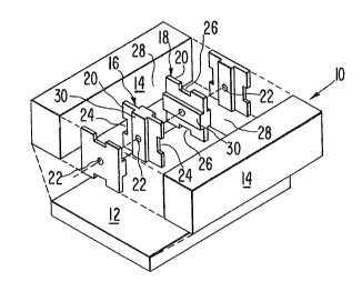
FIG. 1 is an exploded isometric sketch of the circuit parts
before final assembly.
FIG. 2 is a graph of the dispersion characteristics of double-
staggered circuits with and without re-entrancy.
., :
-
.: . . . ;
: : . , ' ' ~ . . , ~.
2~`~()1(}6~
Description oï the Pref~rred Embodimellts
FICr. 1 ~hows the essential structure of the invention. The slow-
wave circuit comprises a hollow extended metallic envelope 10,
S preferably of round or square cross-section, showll here as comprising
a flat bottom plate 12, a pair of side plates 14 and a top cover plate
(not shown). Alternate constructions may be used, such as forming
three of the sides from a grooved block. Inside envelope 10 are two
interleaved sets of "rungs" 16,18, spaced periodically along the axis.
Each rung 16, 18 comprises a flat plate 20 which substantially closes
off the envelope passageway when the exploded parts in FIG. 1 are
brought together. At the center of each rung 16, 18 is an aperture 22
aligned on-axis for passage of the electron beam. Each rung 16, 18
has a pair of coupling apertures 24, 26 on opposite sides of plate 20,
15 increasing the intercavity coupling and hence, the bandwidth above
that obtainable with sinde apertures. Coupling apertures 24 in the
first set of rungs-16 are at ri~t angles to apertures 26 in the second
set 18 so that the Mvities 28 between rungs lL6, 18 are coupled only
to their immediate neighbors. This improves the shape of the
20 bandpass characteristic.
Each rung 16, 18 has a pair of parallel ~idges 30 on its ~aces,
surrounding beam apertures æ and extending across rungs 16, 18 at
right angles to the direction from beam aperture æ to coupling
apertures 24, 26. The function of ridges 30 is to increase
25 the interaction impedance and hence, efficiency and bandwidth of the
travelling wave tube. For good efEIciency the gaps between successive
beam apertures æ must be kep~ short so that electrons cross it in a
~action of an rf cycle before the electric field changes substantially.
Since this is a backward-wave circuit, each electron should be in the
~ ~n
.
, ., ~ ' ' ` ~
:
20()~(~67
shielded interior of an aperture hole 22 while the fiekl is reversing, so
that the electron is exposed to fields in the same phase as it crosses
successive gaps. In addition, the electric Flelds are concentrated in the
region of the beam by the action of the parallel ridges 30, thereby also
S increasing the interaction impedance. The interaction impedance
improvement per se could be achieved by simply making the rungs
thicker, but this would decrease the "cold" bandwidth and not
concentrate the electric fields in the region of the electron beam. [ he
"hot" bandwidth depends on, ~lrst, the degree of coupling between
10 adjoining circuit elements (essentially resonant ca~rities) and, secondly~
the characteristic impedance of the individual cavity elements between
rungs, often referred to as R/~. In the lumped-circuit analogy, R is
the interaction impedance at resonance and Q is the ratio of rf energy
stored to energy extracted per radian. Putting the rung surfaces closer
15 together increases their mutual capacitance and hence the energy
stored for a given interaction voltage between them.
1~e ridges 30 on rungs 16, 18 shorten the interactior. gaps as
described above. Since opp~sed ridges 30 cross each other
transversely, the area of short gaps is much less than if the entire
20 rungs were thicker, sa the capacitance is decreased and bandwidth is
increased. In low-frequencJ~ tubes with easily machinable parts, this
result is sometimes produced by apertured conical noses projecting
from the cavity walls. In the dimensions reguired for millimeter
waves, these would be prohibitively hard to manufacture and assemble,
25 so the ridges of~er a reasonable solution.
Rungs 16, 18 preferably have a square overall outline. They
are then identical in shape, simplifying manufacture. Final assembly
involves aligning them with alternating rotations and brazing to the
- surrounding envelope bottom 12, side 14 and top ~not shown) plates.
cc cn
20(~ 67
FIG. 2 illustrates the advancement in TWT bandwidth achieved
by the invention It is a graph of tllc dispersion diagram of slow-wave
circuits in which ~requency (ordinate) is plotted against ~ T (abscissa)
which is the phase change in half-cycles per ~periodic length of the
5 circuit
The upper curve 40 is from data on a prior-art, non-reentrant~
double-staggered ladder circuit as described in aforementioned U.S.
Patent No. 4,409,519 The rungs of that invention are llat slabs. The
total "cold" bandwidth between bandedge cutoff frequencies is 105
10 GHz or 9 4% of the center frequency.
Lower curve 44 is data frorn the re-entrant, double-staggered
ladder circuit of the present invention The total bandwidth is 165
GHz or 14 2% of the center frequency, an increase of 50% in
percentage bandwidth.
The usable operating bandwidths are those portions over which
~e dispersion curves are substantially linear so that the circuit waYe
can be synchronous with a fixed electron velocity These are quite
proportional to the total "cold" bandwidths listed above
The preferred embodiment described above is exemplary and
20 not limi~ng. Other embodiments within the scope of the invention will
be obvious to those skilled in the art. The invention is to be limited
only by the following claims and their legal equivalents
c~
,