Note: Descriptions are shown in the official language in which they were submitted.
200~ S
1070-430
Title: ELE~TROSTRICTIVE A~TUATORS
BACKCROUN~ AND F_ELD C!~F T~E ~N~UTION
The present invention is directed to the field of
ceramic actuators and capacitors and relates more
particularly to a ceramic capacitor or aotuator having
improved mechanical characteristics. and where used as an
actuator having improved e~pansion characteristics and
resistance to breakage after repeated cycles of use. Still
more particularly. the invention hereof is directed to a
method of manufacturing an actuator or capacitor Or the t~pe
described. For conveniencel the method and article of the
instant lnvention will be referre~ to as a ceramic actuator
or actuators. As used herein, such term is intended to
encompass ceramic ca~acitors.
PRIOR ART
Actuator devices which are comprised of
electrostrictive elements are well known in the industry and
are used inter alia in printer heads of impact printers, the
force generating elements of relays, and as means for
deflecting or forming optical surfaces to vary the
characteristic thereof. Such actuator devices may take the
form Or two or more ceramic layers. and generally a
multiplicity of such layers. the layers having interspersed
therebetween eleotrode areas. As is conventional, in order
to facilitate connection of electrodes of the same polarity
without shorting between the electrodes of adjacent layers~
it is common practice (for capacitors or actuators) to form
a stack of green ceramic sheets wherein the electrode areas
of opposite polarities exit at different surfaces Or the
~k
2001435
stack. Thus, in the case of a rectangular shaped actuator,
electrodes of a first polarity may be exposed at the left
hand side of thæ stack and intervening electrodes of
opposite polarity may exit from the right hand 5ide of the
stack. In order to facilitate for~ing electrical
connections between electrodes of the same polarity, it is
common practice Sor the sheet forming the stack to be coated
with electroding material such that the electrode area
extends to one margin of the stack but terminates short Or
the opposite margin of the stack. Since the resultant stack
e~poses electrode of only one polarity at each of `the
respective two sides. it is possible to apply a conductive
termination to entirety of the two sides which termination
will make electrical contact with the electrodes which are
exposed but which will be isolated from the electrocles of
opposite polarity due to the presence of unelectroded
ceramic areas intervening between e~posecl electrodes.
While the described structure represents virtually the
entirety Or ceramic MLC's used by the industry, devices of
the type described incorporate drawbacks especially where
used as actuators, i.e. for their electrostrictive property,
but also where used in conventional capacitor applications.
More particularly, the drawback derives from the fact that
the finished actuator includes a ceramic to ceramic bridging
connection between adiacent dielectric layers in the areas
where there is no intervening electrode material between the
layers.
The layer to layer cera~ic ~onding has been found to
drastically restrict or constrain the ability of the ceramic
device to expand in a direction perpendicular to the plane
of the dielectric layers. In additionl actuators fabricated
in accordance with the conventional methods described have
20~435
evidenced a significant tendency to crack or split after
protracted use. The tendency to split is also present in
ceramic capacitors not employed as actuators, a tendency
which is beIieved to result from the fact that virtually all
ceramic compositions have some degree of electrostrictive
property, and thus are subject to dimensional ohanges when
voltages are applied.
In order to avoid the constraining` influences of areas
Or ceramic bridging from layer to layer~ while at the sa~e
time providing means for terminating the act~ator. the prior
art has proposed solutions which while e r fective are
difficult to i~plement on a commercial scale.
U.S. Fatent 4,52~,121 Or June 11. 1985 (Takahashi)
describes a multi-layer electrostrictive device capable of
enhanced expansion characteristics and of withstanding
repeated pulsing. This rererence notes the constraining
influence of hridging areas of ceramic between dielectric
layers and it proposes, as a solution, formation of an
essentially conventional electrostrictive device which is
modified by cutting away the bridging ceramic areas between
adjacent layers as by the use Or a diamond cutter. tColumn
11 lines ~ and following). The noted reference also suggest
forming the basic actuator block with the electrodes of both
polarities extending to the extremities of the block,
thereafter applying areas of insulation in registry with the
edge portions of alternate layers at opposite sides of the
block and thereafter forming a termination over the
insulating portions.
Patent 4,~81,667 of July 21, 1987 tUtsuni) describes
the method of manufacturing an electrostrictive device by
forming a monolith of alternate ceramic and electrode
layers. Electrodes of a first polarity are electrically
200~4~5
connected and the device i5 immersed in a bath containing
charged glass insulating particles which are attracted to
the exposed portions of the e]lectrodes remote from the
initial connection. The process is repeated with the
electrodes of opposite polarity whereby there is for~ed
surfaces at opposite portions of the monolith wherein only
electrodes of a given polarity are exposed. Terminations
may thereafter ~e erfected to the surfaces without fear of
terminating material shorting electrodes of opposite
polarities.
As will be evidences from a re~iew of the noted prior
art devices, the proposed solutions are of questionable
commercial viability. Obviously. in view of the fact that
the dielectric layers may be less than a mllimeter in
thickness an~ that a large number of layers may be employed
in a single actuator the ability to form cuts with a diamond
sa-~ or to accuratelv paint insulation~ or to deposit
insulating materials, in precise registry with electrodes at
opposite sides of the monolith represents a significant
investment in labor and results in a substantial cost
increase.
Other references found in a search of the prior art and
of limited or no relevance include the following U.S.
Letters Patent:
4,6b7,1~7 May 19, 1987
4,654,546 March 31, 1987
4,527,~82 July 2, 1985
3,967,027 June 29, 1976
3,943,bl4 March 16, 1976
3,940,974 March 2, 1976
3 ? 27~,031 September 27. 1966
2,478?22~ August 9, 1949
200~4.~
SUnn~RY OF THE INVENTION
The present invention is ~directed to a metho~ of
manufacturing an actuator device which is free of dielectric
to dielectric connection between adjacent layers. The
method of the invention provides an economical and
commercially feasible means for forming an actuator of the
type described wherein electrodes of opposite polarity are
exposed at opposite faces of the ceramic monolith whereby a
termination may be applied to the entirèty of such faces
without fear of short circuiting layers of opposite
polarity. The method of the present invention. for the
first time, describes a practical means of forming a ceramic
electrostrictive actuator device wherein a large numher of
thin dielectric layers are present.
More specifically, the method of the ~resent in~ention
involves providing a number of sheets of "green" ceramic
material which are imprinted with a pattern of arèas of
electrode forming materials and other areas of "pseudo-
electrode" for~ing material. The term "pseudo-electrode" as
used herein is intended to refer to a material which adds
bulk so as to provide a divider and which i 5 subiect to
volitilization in the course of fabrication of the ceramic
monolith. Pseudo-electrode inks are known per se as, for
example, from U.S. Patent 3,67~,95~.
In accordance with the method of the invention thæ
green ceramic sheets have imprinted thereon, as by silk
screening or the like, a metalized ink, i.e. an ink
including platinum or palladium particles. The metalized
ink extends to at least one margin of the sheet. The
remainder of the sheet is imprinted with a pseudo-electrode
forming ink, the pseudo-ink extending to at least one other
margin Or the sheet. A plurality of the sheets of green~
- . ~
20~ 3~i
imprinted ceramic are stacked in such manner that the edges
of the metalized electrode layers of the odd numbered sheets
are exposed at a first surface Or the s~ack and the
metalized electrode edges Or the intervening layers are
exposed at a second edge surface Or the stack. Between each
pair of exposed end portions Or the metalized electrodes
there is disposed a portion Or a sheet having pseudo-
electrode materials exposed at the edge and extending a
distance inwardly towards the interior Or the stack.
Following burn-out and sintering Or the stack, the
pseudo-electrode material is driven off with the result that
the two noted surfaces of the stack are comprised Or expose~
electrodes of the same polarity with intervening voids in
the area previously occupied by the pseudo-electrode
material. As a result, a conductive termination may be
applied to the noted surfacesl the termination making
contact with only electrodes of a given polarity. Since the
termination material does not penetrate into the interior Or
the stack in the areas of the voids, the termination
material cannot short circuit to electrodes of opposite
polarity. Additionally, since the pseudo-electrode ~aterial
leaves a void in the area between adjacent dielectric
sheets, there is no signirioant bonding between the sheets
~hereby the adjacent dielectric layers are ~ee to expand
without interference.
The resulting actuator device will expand by a factor
2~/. or more times the amount of expansion available i~ the
adjacent layers were in ceramic to ceramic contact.
An important advantage Or an actuator or capacitor made
by the noted method is that the device is far more resistant
to breakage at the cleavage limes between layers~ This is
50 since the unconnected layers are free of the tendency to
~ :200~4~5
fle~ or bend when subiected to applied voltages as is the
case with conventional actuators or capacitors wherein the
edge portions are bonded together and the central portions,
wherein the electrodes are in registry, are free to expand.
The invention is further directed to an article of
manufacture comprised of a green ceramic stack formed in
accordance with the method hereinabove described.
lt i5 accordingly an ohject Or the invention to provide
a method of manufacturing multilayer ceramic actuat.ors ancl
capacitors which are essentially free of ceramic to ceramic
connections in adjacent layers and which may be readily
terminated by conventional terminating techniques. A
further object of the invention is a provision of a method
of type described which may be reaclily practioed on a
commercial scale.
BRIEF DESCRIPTIO~ OF THE DRAUI~GS
. _ . ... ... .. .. _ _ , , , ,, , _,
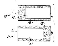
Fig. 1 re~resents a diagrammatic plan view of a pair of
green ceramic sheets coated with a combination of electrode
forming ink and pseudo-electrode ink in accordance with the
invention.
Fig. 2 is a diagrammatic sectional view of a stack of
the sheets as shown in Fig. 1.
Fig. 3 is a view similar to that of Fig. 2 showing the
stack of Fig. 2 after burnout and sintering.
Fig. 4 is a view similar to Figs. 2 and 3 following
application of termination.
~ETAILE~ DESCREPT O~ _ F PRO OE-~
Referring now to the drawings which are diagrammatic in
nature, there is shown in Fig. 1 a pair of green ceramic
sheets 1~,11 which are essentially identical in size. It
~ill be recognized by those skilled in the art that the
sheets 1~,11 in commercial practice will comprise segments
.
`` 200~4~35
of a larger sheet or band of green ceramic which sheet or
band has been simultaneous1y imprinted ~ith a multiplicity
Or printing areas from which sheets such as sheets 10 and ll
are stamped and subsequently stacked.
In accordance with the method of the invention, the
sheets are imprinted with an electroding patt.ern, the area
12 Or the sheets being imprinted with a conventional
electroding ink more fully described hereinafter, but
basically comprising a solvent, a binder, and particulate
metal such as platinu~, gold, or ~alladium resistant to the
high temperatures of sintering.
As will be apparent, the sheets l~. 11 are identical
but have been reversed one with respect to the othe~. The
electrode forming ink component 12 extends to an end margin
13 of the sheet 1~ and to the o~posite end margin 14 of the
sheet 11. As see in Fig. 1, the remaining area of the
sheets 10 and 11 surroundin~ the electrode areas 12 is
generally U-shaped as shown at 15. the U-shaped areas 15
being coated by a "pseudo electrode" forming ink composition
16. Suitable pseudo ink formulations are known. i.e. from
patents such as U.S. patent 3,679,95~ dealing with the
formation of a capacitor by a process of forming voids
within a ceramic monolith using pseudo ink, and thereafter
filling the voids with molten lead to define electrodes.
The pseudo-electrode ink which in general is comprised of
organic materials which burn out in a heated environment
junction to assure that void areas are present between the
ceramic layers after sintering.
While the respective coatings as disclosed in Fig. 1
have been shown as comprising a central area 12 coated with
electrode forming ink and a generally U-shaped surrounding
area 15 coated by pseudo ink lb, it should be appreciated
. - .
., .
20~43S
that the geometry of the coatings may be varied. More
particularly, the electrode ink area 12 may e~tend across
the entirety of the sheet rather than being surrounded by a
pseudo electrode area which is U-shaped in plan. All that
is necessary for the satisfactory exploitation of the method
is that the electrode area 12 extend to one margin 13 of the
sheets, and that the pseudo electrode area extend to a
separate margin, i.e. 17 of the sheets. Alternate geometric
arrangements of the electrode ink and pseudo electrode ink
may readily suggest themselves to those skilled in the art.
By way of example. and without limitation~ it would be
feasible to form an actuator in the configuration of a
cylinder having a through going central aperture. In this
configuration the odd num~ered sheets may have electrode ink
extending from the central aperture toward the clrcumference
but terminating short of the circumference whereas the even
numbered s~eet would have electrode areas extending from the
circumference toward but terminating short of the central
aperture. In all cases. the areas Or the sheets not covered
by electrode ink are covered by pseudo electrode ink.
Returning to the geometry of the illustrated
embodiment, there is shown in Fig. 2 a stack of sheets 1~
and 11 arranged in such manner that the margins 13 of
alternate sheets extend to one end surface 18 and the margin
14 of the sheet intervening between the alternate sheets
extend to an the opposite surface of the stack. It will be
further observed that the resulting stack includes margins
17 of exposed psuedo-ink disposed between each of the
margins 13 or 14 having exposed electrode materials at the
respective sides 18 and 19 of the stack.
In Fig. 3 there is disclosed the configuration of a
finished actuator formed as a result of sintering the green
i
200:1~35
1~
ceramic stack of Fig. 2. As will be apparent ~rom ~ig. 3.
edge portions 2~ of the ~dd numbered electrodes ~1 will be
exposed at the end 18 of the actuator and edge portions 22
of the even numbered electrodes 2~ will be exposed at the
ends 1~ of the monolith. Due to the volitilization Or the
pseudo ink components, void areas 24 will be disposed at the
end of the monolith between the exposed ends ~ and 21 of
the electrodes.
As sh~wn in Fig. 4, conductive terminations 25, ~6 may
accordingly be applied over the respective ends ln,l9 of the
monolith which terminations will make contact with
electrodes of only a single polarity. Thus, the termination
25 connects the odd numbered electrodes 21 whereas the
termination 2~ i 5 connected to the even numbered electrodes
23.
Optionally~ the respective sides 1~ and lq of the
monolith may be processed to inject insulating materials 27
into the voids Z4 before application of the termination.
Normally, however. the use of ins~lating material such as
elastomers or epoxies is not necessary due to the depth of
the void areas 24.
An important feature of the invention resides in the
fact that due to the volitilization of the pseudo electrode
forming ink, there is no significant ceramic to ceramic
contact between adiacent dielectric layers. The absence o~
such bridging ceramic contact betwæen layers permits the
finished actuator to expand without constraint in a
direction perpendicular to the plane of the dielectric and
electrodes. It has been experimentally determined that the
absence of bridging areas of cera~ic between adjacent
dielectric surfaces permits an expansion of the actuator by
factor of 2~% or more greater with the same input voltage
20014:~S 1 1
voltage than is the case with conventional actuators. A
further advantage of actuators fahricated in accordance with
the method of the present invention resides in their greater
resistance to breakage following repeated pulsing. It i5
theorized that the increased life cycle of the actuators
fabricated in accordance with this invention resides from
the fact that the dielectric layers are subiected to minimal
flexing or ~ending in contrast with conventional actuators
wherein the edge port.ions are constrained by cera~ic to
ceramic contact and the central portions e~pand upon
application of voltages. It should be observed that in the
course of the sintering process~ it is inherent that an
occasional pillar or grain will gl`OW through from one layer
to the next even in the areas previously occupied bv the
pseudo electrode ink. However. the presence of such
oocasional pillars does not ma~erially affect the ability of
the dielectric layers to shift relative to each other in a
di~ection normal to the plane Or such layers, and the
constraint against such e.Ypansion engendered by such
occasional pillars is minimal.
PROCESS DESCRIPTION DETAILS
__ __ _ . .... _ . . _ . _ ... . . _ .. . .
In order to comply with the "best mode" requirements of
the Patent Laws there will be hereinafter described details
of the rormulations and handling steps employed in the
fabrication of the actuators in accordance with the
invention. It should. however, be noted that the process is
carried out utilizing materials all of which are well known
in the p-rior art including specifically the dielectric
formulations and methods Or processing same, the pseudo ink
formulations, the electroding ink formulations, and the
-` 200~435
12
termination formulations and mode ~f application. By way of
example and without limitation a preferred method is
practiced as follows:
A. DIELE~CTRIC MATERIAL
A dielectric material mass was formulated as
follows ~all figures being given by way of percentage
weight):
~8.2~/. Lead Oxide (PbO)
27.4'~. Columbite ~MgNb=O~)
1.2% Barium Carbonate ~BaCO~ ~Binder)
~.4% Titania ~TiOr) ~Binder~
The ingredients are mixed and milled to an average
particle size Or 1 micron, and blended with a solvent and
binder formulation comprised as follows:
1.75% Fish Oil
12.9 % Xylene
8.2~/. Ethanol
2.44~/. Poly-vinyl Butyrol
2.71~/. UC0~-2~ Union Carbide)
2.25% PX-316 ~Aristec)
The organic carrier system hereinabove described
is merely representative and may be varied as is known in
the art. The particulate materials and binder system are
mixed to form a viscous liquid composition the viscosity of
which may be varied in accordance with the thiokness of the
tape to be cast. A tape i 5 cast on a belt running under a
doctor blade or blades to a thickness Or substantially 8
mils. After excess solvents are evaporated the tape is
imprinted with the pattern as described utilizing electrode
inks and pseudo inks. The composition of the respective
200~40~5 , 3
inks is not critical a suitable electruding ink being
identified as number R~3~1 which is obtained from the
Johnson-Matthey Corporation.
A suitable pseudo ink or fugitive ink i5
formulated as set forth in above referenced U.S. patent
3,679,95~. A suitable pseudo ink may be formed from a
squeegee medium prepared by mixing 8~ mililiters of pine
oil, 14 grams of acrylic resin and 1.5 grams of lecithin.
1~ grams of this mixture are blended with 12 grams of the
calcined ceramic formulation set forth above ~average
particle size Or about 4 microns), 4 gra~s of carbon black~
and 1.5 grams of ethyl cellulose. Cap Stoddard solvent or
equivalent is added until a viscosity suitable for printing
is achieved.
The fabrication procedures are conventional and
involve application of electrode ink through a mesh screen
patterned in accordance with the size and positioning of the
multiple electrode areas. The electrode ink i 5 allowed to
dry and the sheet in overprinted using a mask which is the
negative of the mask employed to lay down the electrode ink.
A number of sheets each carrying a multiplicity of
imprinted areas are stacked i~ registry and the stack is
la~inated at about 65C~ at about 15~ pounds per square
inch. The stack is removed from the press and allowed to
cool. Thereafter the stack is diced so as to form from the
stacked series of large sheets a multiplicity of individual
green actuators as shown in Fig. 2 hereof. The individual
units are separated and subjected to a burnout cycle
consisting of 24 hour exposure at a progressively increasing
temperature, the maximum temperature being 5~C. The parts
are fired in a sintering kiln at a maximum temperature of
115~C for three hours.
201~14~5
14
The end surfaces of the parts, after c~oling, are
terminated with any of a series of co~ventional silver-glass
frit compositions. A representative suita~le composition
may be identified as Dupont ~1~4 the ~rit being thereafter
fired in a belt furnace throug~ an approximately half hour
cycle, three minutes of such cycle being at the maxim~m
temperature of 75~C. ~he finished actuators thereafter
have a lead soldered thereto or may be solder coated
depended upon their intended end use and configuration. The
actuators may be further processed as by encapsulation in an
epoxy or elastomeric matrix again depending upon whether the
end product is to be used as a capacitor or actuator.
Alternate terminations such as conductive polymers or
elastomers may be used where extreme expansion or frequent
cyclin~ is anticipated.
As will be apparent from the preceding detailed
description of a specific embodiment, the selection of
formulations for the dielectric, the electrode ink or paste,
the fugitive "pseudo-electrode" ink, and the termination
materials, as well as the mode of processing the same are
all well known in the art. The invention hereof is
considered to reside in the concept of employing the
co~bination of an electroding ink and a pseudo electroding
ink in such manner as to provide a monolithic device wherein
electrodes of opposite polarity exit from difference
surfaces of the monolith, wherein voids are present between
electrodes of like polarity, and wherein the dielectric
layers are essentially unconnected one to the other the sole
significant iunction between such layers being the areas
linked by the electrodes.
As will be apparent from the preceding description,
numerous variations in details of geometry, formulation and
200~43~
struct~re will occur to those skilled in the art a~d
familiarized with the instant disclosure. AccordinglyJ the
invention is to be broadly construed within the scope of the
appended claims.