Note: Descriptions are shown in the official language in which they were submitted.
- 2~2
- 1 -
This invention relates to a thin film transistor
having a memory function and a method for using a thin
film transistor as a memory element.
As is well known in the art, a thin film transistor
includes a gate electrode, a gate insulation film, a
semiconductor layer and source and drain electrodes
which are formed in a laminated structure. The stagger
type, inverted stagger type, coplanar type and inverted
coplanar type structures are known as the thin film
transistor.
The conventional thin film transistor has no memory
function. Further, a method of using the thin film
transistor as a memory element is not known in the prior
art. However, it is extremely convenient if the thin
film transistor has a memory function.
This invention has been made in view of the above
fact, and an object of this invention is to provide a
thin film transistor having a memory function and a
method for using a thin film transistor as a memory
element.
The above object can be attained by a memory ele-
ment comprising a thin film transistor having a semicon-
ductor layer-~4t; a source electrode-(G~-electrically
connected to the semiconductor layer; a drain electrode
-~t electrically connected to the semiconductor layer
and formed separately from the source electrode; a gate
electrode (2) for controlling formation of a channel;
;~
-- 2
and insulation film means (3) for isolating the gate
,.,
electrode ~ from the semiconductor layer t~t~and caus-
ing a hysteresis in the relation between the drain cur-
rent and the gate voltage.
The insulation film means includes an SiN film
having a composition ratio Si/N of silicon atoms Si to
nitrogen atoms N which lies in a range between approx.
0.85 and 1.1.
According to this invention, the gate insulation
film means causes a hysteresis in the gate voltage-drain
current relation. The thin film transistor may have a
memory function due to the hysteresis of the gate
voltage-drain current relation and as a result the thin
film transistor can be used as a memory element.
Further, the above object can be attained by a
method for using a thin film transistor as a memory
element comprising the steps of preparing a thin film
transistor having a semiconductor layer ~, a source
electrode t~t, a drain electrode -~7~, a gate electrode
^~ and a gate insulation film; writing first data into
the thin film transistor by applying a first voltage to
the gate insulation film; writing second data different
from the first data by applying a second voltage of
a polarity opposite to that of the first voltage to the
gate insulation film; and reading data stored in the
thin film transistor according to a current which
flows in the channel and whose level is changed by
a difference in the voltages applied to the gate insula-
tion film.
According to this invention, data can be written
into the thin film transistor by applying an adequate
voltage to the gate insulation film and then the data
can be read out from the thin film transistor. That is,
the thin film transistor can be used as a memory
element.
This invention can be more fully understood from
the following detailed description when taken in con-
junction with the accompanying drawings, in which:
Fig. lA is a cross sectional view of a thin film
transistor having a memory function according to a first
embodiment of this invention;
Fig. lB is a plan view of the thin film transistor
according to the first embodiment;
Figs. 2A and 2B are cross sectional views showing
the manufacturing process of the thin film transistor
according to the first embodiment;
Figs. 3A to 3D are graphs showing the relation
between the VG-ID characteristic and the composition
ratio of Si/N of the gate insulation film of the thin
film transistor with the thickness of the gate insula-
tion film set at 2000 angstrom;
Figs. 4A to 4D are graphs showing the relation
between the VG-ID characteristic and the composition
ratio of Si/N of the gate insulation film of the thin
~Z~i~32
-- 4
film transistor with the thickness of the gate
insulation film set at 3000 angstrom;
Fig. 5 shows the relation between the degree of
hysteresis and the composition ratio of Si/N of the gate
insulation film of each of the thin film transistors in
a case where the gate insulation films are formed to
have thicknesses of 2000 and 3000 angstrom;
Figs. 6 to 8 are cross sectional views showing the
structures of applications of the thin film transistor
used for a memory and according to the first embodiment;
Fig. 9 is a cross sectional view showing the struc-
ture of a thin film transistor constituting a memory and
according to a second embodiment of this invention;
Figs. 10 and ll are graphs respectively showing the
relation between the film thickness of a non-memory
insulation film of the thin film transistor of Fig. lO
and the leak current and that between the film thickness
and the hysteresis width;
Fig. 12 is a cross sectional view showing the struc-
ture of a thin film transistor having a memory functionaccording to a third embodiment of this invention;
Figs. 13 to 15 are cross sectional views of appli-
cations of the third embodiment of this invention;
Fig. 16 is a cross sectional view showing the
structure of a thin film transistor having a memory
function according to a fourth embodiment of this
invention;
~'~
Fig. 17 is a graph showing the characteristic of
the thin film transistor with the memory function
according to the fourth embodiment;
Fig. 18 is a cross sectional view showing the
structure of a thin film transistor having a memory
function according to a fifth embodiment of this
invention;
Fig. l9A is a cross sectional view of a thin film
transistor according to a sixth embodiment of this
invention;
Fig. l9B is a plan view of the thin film transistor
of the sixth embodiment;
Fig. 20 is a view showing a model of the structure
of a gate insulation film of the thin film transistor
according to the sixth embodiment;
Figs. 21A to 21D are cross sectional diagrams
showing the manufacturing process of the thin film
transistor according to the sixth embodiment;
Fig. 22 shows the relation between the flow rate
ratio of silane gas SiH4 to ammonia gas HN3 and the
composition ratio (Si/N) of silicon atoms Si to nitrogen
atoms N in the deposited silicon nitride film.
Fig. 23 is a diagram showing the characteristic of
the thin film transistor according to the sixth
embodiment; and
Figs. 24 and 25 are circuit diagrams of examples of
memory circuits using the memory element of this
-- 6
invention.
There will now be described a first embodiment of
this invention with reference to the accompanying
drawings.
Fig. lA is a cross sectional view of a thin film
transistor having a memory function according to the
first embodiment and Fig. lB is a plan view of the thin
film transistor shown in Fig. lA. Fig. lA corresponds
to a cross sectional view taken along line A-A of
Fig. lB. In Fig. lB, only main portions are shown for
easy understanding the positional relation thereof.
In the first embodiment, the thin film transistor
with the memory function has an inverted stagger type
structure. The basic structure of the thin film tran-
sistor with the memory function is the same as that of
the conventional inverted stagger type thin film tran-
sistor. However, the film quality (composition) of the
gate insulation film of the thin film transistor of this
embodiment is different from that of the gate insulation
film of the conventional thin film transistor.
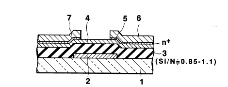
The structure of the thin film transistor with the
memory function is now explained with reference to
Figs. lA and lB. A gate electrode 2 of chromium, Al or
the like is formed on an insulation substrate 1 of
glass, for example. A gate insulation film 3 is formed
on the gate electrode 2. A semiconductor layer 4 of i
(intrinsic)-a (amorphous)-Si (silicon) structure with
-- 7 --
a thickness of approx. 300 to 600 angstrom is formed on
the gate insulation film 3. The semiconductor layer may
be formed of polycrystalline silicon, monocrystalline
silicon or compound semiconductor, for example.
Further, n+-a-Si contact layers 5 of N-type high impu-
rity concentration are formed on the semiconductor layer
4 and source electrode 6 and drain electrode 7 are
formed on the n+-a-Si contact layers 5. The presence of
the contact layer 5 permits an ohmic contact to be
obtained between the semiconductor layer 4 and the
source and drain electrodes 6 and 7.
The gate insulation film 3 is formed of an SiN film
having a hysteresis characteristic. More specifically,
the gate insulation film 3 is formed of an SiN film with
the composition ratio Si/N of silicon atoms Si to nitro-
gen atoms N which is set larger than the stoichiometric
ratio (Si/N=0.75). In this embodiment, the film thick-
ness of the gate insulation film 3 is set at approx.
2000 angstrom and the composition ratio thereof is set
at 0.85 to 1.1.
Now, the manufacturing process of the thin film
transistor with the memory function is explained with
reference to Figs. 2A and 2B. First, a metal film MF1
is formed to a thickness of approx. 500 angstrom on the
insulation substrate 1 by the sputtering or CVD method.
After this, a photoresist film is formed on the metal
film MFl which is then etched out as shown in Fig. 2A.
x~
-- 8
The film MFl is patterned with the remaining photoresist
film REl used as a mask so as to form a gate electrode.
Then, an SiN film constituting the gate insulation film
3, i-a-Si semiconductor layer 4 and n+-a-Si contact
layer 5 are sequentially formed on the resultant struc-
ture by the plasma CVD method. Further, a metal film or
photoresist film MF2 is formed on the resultant struc-
ture and a photoresist film is formed on the film MF2.
The photoresist film is etched out as shown in Fig. 2B.
The film MF2 is patterned with the remaining photoresist
film RE2 used as a mask so as to form a source electrode
6 and a drain electrode 7. Further, that portion
(channel portion) of the contact layer 5 which lies
between the source electrode 6 and the drain electrode 7
is etched out with the photoresist film RE2 used as a
mask. As the result of this, the structure shown in
Fig. lA is obtained.
Formation of the SiN film constituting the gate
insulation film 3 by use of the plasma CVD method is
effected by selectively setting the flow rate ratio of
SiH4 to NH3 used as the main component gases in the
process such that the composition ratio Si/N of an SiN
film to be formed can be set within the range of 0.85
to 1.1. For example, the flow rate ratio of SiH4 to NH3
is set to 42:48. The gate insulation film (SiN film)- 3
has a sufficiently large hysteresis characteristic.
Figs. 3A to 3D show the result of measurement made
2~D0~8;~
for the VG-ID characteristic (the relation between the
gate voltage VG and the drain current ID) of the thin
film transistor with the film thickness of the gate
insulation film (SiN film) 3 set at 2000 angstrom in a
case where the composition ratio of Si/N of the gate
insulation film 2 is changed.
Fig. 3A shows the VG-ID characteristic in a case
where the composition ratio Si/N is set at 0.75 (which
is the composltion ratio of Si to N when the gate insu-
lation film of the conventional thin film transistor is
formed of Si3 N4), Fig. 3B shows the VG-ID characteris-
tic in the case of Si/N=0.85, Fig. 3C shows the VG-ID
characteristic in the case of Si/N=l.0 and Fig. 3D shows
the VG-ID characteristic in the case of Si/N=l.l.
Figs. 3A to 3D show the result of measurement of
variation in the drain current (current flowing in the
channel between the source electrode and the drain
electrode) ID with respect to the gate voltage VG with
the drain voltage VD set at 10 V.
AS is clearly understood from Figs. 3A to 3D, the
VG-ID characteristic of the thin film transistor in
which the gate insulation film is formed of the SiN film
having the composition ratio of Si to N of 0.75 displays
little hysteresis.
In contrast, each of the characteristics of the
thin film transistor in which the gate insulation film
is formed of the SiN film having the composition ratio
~o~
-
-- 10 -
of Si to N of 0.85 to 1.1 displays a relatively large
hysteresis as shown in Figs. 3B to 3D.
In Figs. 3A to 3D, the degree of delta vth of the
hysteresis is defined as a difference between the gate
voltage VG at which the drain current ID becomes 1 nA
when the gate voltage vG is gradually changed from a
negative value to +40 v and the gate voltage vG at which
the drain current ID becomes 1 nA when the gate voltage
VG is gradually decreased from +40 V. delta Vth=2 v in
Fig. 3A, delta vth=14 v in Fig. 3B, delta Vth=28 v in
Fig. 3C, and delta Vth=20 V in Fig. 3D.
As described above, the VG-ID characteristic has a
relatively large hysteresis characteristic as shown in
Figs. 3B to 3D, and this means that the thin film tran-
sistors have the memory function in which charge can bestored in the gate insulation film 3. Therefore, the
thin film transistor whose gate insulation film 3 is
formed of an SiN film having the composition ratio of Si
to N of 0.85 to 1.1 can be used as a memory element in
which data can be written or read out by controlling a
voltage applied to the gate electrode 2. Further, the
thin film transistor with the memory function maintains
the influence by a voltage which is finally applied to
the gate electrode 2. Therefore, the thin film transis-
tor can be used as a memory element such as an E 2 PROM.
In the above explanation, delta Vth is called "thedegree of hysteresis", but delta vth may be called "the
size of hysteresis", "hysteresis width" or "memory
width".
Further, in the above explanation, the film thick-
ness of the SiN film used as the gate insulation film 3
is set at 2000 angstrom. However, the film thickness of
the SiN film can be selectively set in a range of 500 to
4000 angstrom. It is preferable to set the film thick-
ness in a range of 2000 to 3000 angstrom (which is the
thickness of the gate insulation film of the ordinary
thin film transistor). In a case where the film thick-
ness of the SiN film is made larger, it becomes neces-
sary to make the range of the Si/N composition ratio
narrower than that (Si/N=O. 85 to 1.1) set in the case of
the film thickness of 2000 angstrom.
Figs. 4A to 4D show the result of measurement (made
by setting the drain voltage VD at 10 V and the source
voltage Vs at 0 V) of the VG-ID characteristic of the
thin film transistor with the film thickness of the gate
insulation film 3 set at 3000 angstrom in a case where
the SiN composition ratio of the gate insulation film 3
is changed. Fig. 4A shows the characteristic in the
case of Si/N=0.75, Fig. 4B shows the characteristic in
the case of Si/N=O. 85, Fig. 4C shows the characteristic
in the case of Si/N=l.O and Fig. 4D shows the character-
istic in the case of Si/N=l.l.
As shown in Figs. 4A to 4D, the degree of delta vthof the hysteresis of the VG-ID characteristic in the
- 12 -
case of the gate insulation film having the film thick-
ness of 3000 angstrom is smaller than that of the VG-ID
characteristic in the case of the gate insulation film
having the film thickness of 2000 angstrom shown in
Figs. 3A to 3D even if the composition ratio of Si to N
is set at any value. However, if the Si/N composition
ratio is set at 1.0, a large hysteresis as shown in
Fig. 4C can be attained even when the film thickness is
set at 3000 angstrom. The degree of delta Vth of the
hysteresis shown in Fig. 4C is 16 V. If the degree of
delta Vth of the hysteresis is not less than 15 V, the
thin film transistor can have a practically sufficient
memory function. Therefore, the thin film transistor
having the film thickness of 3000 angstrom and the SiN
composition ratio of 1.0 can be used as a memory element
such as an E2PROM. Delta Vth=0.5 V in Fig. 4A, delta
Vth=2 V in Fig. 4B and delta Vth=12 v in Fig. 4D. The
degree of the hysteresis of Fig. 4D is relatively large.
Fig. 5 shows the relation between the SiN composi-
tion ratio of the SiN film and the degree of delta Vthof the hysteresis in cases where the film thickness of
the gate insulation film (SiN film) 3 is set at 2000 and
3000 angstrom. Fig. 5 shows the result of measurement
of delta Vth at which a circuit of 1 nA flows between
the source and drain when the gate voltage VG is set at
+ 40 V, the drain voltage is set at lO V and the source
voltage is set at 0 V. As is understood from Fig. 5,
2~ 8~
- 13 -
the hysteresis becomes largest when the composition
ratio of Si to N is set at or near l.0 irrespective of
whether the film thickness of the SiN film 3 is set at
2000 or 3000 angstrom. As described before, when the
degree of delta Vth of the hysteresis is larger than
15 V, the thin film transistor can have a practically
sufficient memory function. Therefore, if the film
thickness of the SiN film is set at 2000 angstrom, the
composition ratio of Si to N may be set between
approx. 0.85 and 1.1. Further, if the film thickness
of the SiN film is set at 3000 angstrom, the composition
ratio of Si to N may be set at approx. 1Ø
If the film thickness of the gate insulation film
(SiN film) 3 is set to be less than 2000 angstrom, the
range of the composition ratio of Si to N can be set
wider than that of approx. 0.85 to 1.1. However, if the
film thickness of the gate insulation film 3 is set to
be less than 2000 angstrom, the withstanding voltage of
the insulation film is lowered. Therefore, it is pref-
erable to set the film thickness of the gate insulationfilm 3 within the range of 2000 to 3000 angstrom.
In the above embodiment, the inverted stagger
type thin film transistor is explained. This invention
can also be applied to the stagger type, coplanar type
and the inverted coplanar type thin film transistor.
In this case, if the ratio of Si to N of the gate insu-
lation film 3 is set in the range of approx. 0.85 to 1.1
- 14 -
and the film thickness of the gate insulation film (SiN
film) 3 is set such that the degree of delta Vth of the
hysteresis is more than 15 V, then the thin film tran-
sistor may have the memory function.
Fig. 6 shows an embodiment in which this invention
is applied to a stagger type thin film transistor,
Fig. 7 shows an embodiment in which this invention is
applied to an inverted coplanar type thin film transis-
tor and Fig. 8 shows an embodiment in which this inven-
tion is applied to a coplanar type thin film transistor.
The thin film transistors shown in Figs. 6 to 8 are
similar to the inverted stagger type thin film transis-
tor shown in Fig. lA except the laminated structure of
the respective layers constituting the transistor.
Therefore, the same reference numerals are attached to
corresponding portions of the transistors and the expla-
nation for the structure of Figs. 6 to 8 is omitted.
As described above, the thin film transistors of
the above embodiments can be used as a memory element
since the gate insulation film is formed of an SiN film
with the composition ratio Si/N of silicon atoms Si to
nitrogen atoms N lying in the range of approx. 0.85 to
1 .1 .
In a case where the semiconductor layer 4 is formed
of intrinsic silicon, the transistor is operated in a
p-channel operation mode when a negative voltage of
approx. -15 V to -17 v is applied to the gate electrode
Q~8~
- 15 -
2, and the drain current ID abruptly increases as shown
in Figs. 2A to 2D and Figs. 3A to 3D.
In order to solve the above problem, a small amount
of impurity may be doped into the semiconductor layer 4.
With this structure, the gate voltage which may
cause the thin film transistor to be operated in the p-
or n-channel operation mode can be shifted. In this
way, the thin film transistor with the memory function
can be easily controlled.
The semiconductor layer 4 is not necessarily formed
of amorphous silicon and can be formed of the other sem-
iconductor material such as polycrystalline silicon,
monocrystalline silicon or germanium.
Second Embodiment
In the thin film memory element of the first
embodiment, the gate insulation film 3 is formed of an
SiN film having the ratio Si/N =0.85 to 1.15. However,
the SiN film having Si/N=0.85 to 1.15 has an electrical
resistance lower than that of the SiN film having the
stoichiometric ratio of Si/N (Si/N=0.75). For this
reason, a leak current may easily flow between the the
gate electrode 2 and the source and drain electrodes 6
and 7 of the thin film memory element in the first
embodiment. Further, charges injected from the semicon-
ductor layer 4 into the gate insulation film 3 and
trapped therein may tend to be discharged into the gate
electrode 2. In this embodiment, a memory element is
~o~
- 16 -
constituted by a thin film transistor in which the
degree of delta Vth of the hysteresis is increased and a
leak current between the gate electrode and the source
and drain electrodes is suppressed to a small value.
In this embodiment, the gate insulation film is
formed with two-layered structure. The two-layered film
includes a non-memory insulation film having no charge
storage function provided on the gate electrode and a
memory insulation film having a charge storage function
provided on the semiconductor layer.
Now, the second embodiment is explained in detail
with reference to Figs. 9 to 11.
Fig. 9 is a cross sectional view of a thin film
memory element utilizing an inverted stagger type thin
film transistor of this embodiment. The thin film mem-
ory element is formed of an inverted stagger type thin
film transistor having the memory function and formed on
an insulation substrate 11 formed of glass or the like.
The inverted stagger type thin film transistor includes
a gate electrode 12 formed on the insulation substrate
11, a gate insulation film 13 of SiN formed with two-
layered structure and formed on the gate insulation film
12, a semiconductor layer 14 of i-a-Si formed on the
gate insulation film 13, an n-type a-Si layer 15 formed
on the semiconductor layer 14, and source and drain
electrodes 16 and 17 formed on the n-type a-Si layer 15.
Unlike the structure shown in Fig. lA, in the structure
2001682
- 17 -
shown in Fig. 9, the peripheral portion of the
semiconductor layer 14 is formed flush with the
electrodes 16 and 17. The gate electrode 12 and the
source and drain electrodes 16 and 17 are connected to
wirings (not shown).
The gate insulation film 13 is formed of a two-
layered film including a non-memory insulation film 13a
having no charge storage function and a memory insulation
film 13b having a charge storage function and formed on
the insulation film 13a. The non-memory insulation film
13a is formed of an SiN film having the composition ratio
Si/N of silicon atoms Si to nitrogen atoms N set near the
stoichiometric ratio [Si/N=o.75]~ or more generally in
15 the range 0.1 to 0.8, and the memory insulation film 13b
is formed of an SiN film having the composition ratio
Si/N=0.85 to 1.15. The film thickness of the insulation
film 13a is set to 2000 angstrom and that of the
insulation film 13b is set to 100 angstrom.
The above thin film memory element is formed as
follows. First, metal film of chromium (Cr) or the like
is formed to a thickness of 1000 angstrom on the
insulation substrate 11 and is patterned by the
photoetching process (PEP), for example, so as to form a
gate electrode 12. Then, a non-memory insulation film
13a, a memory insulation film 13b, an i-type a-Si
semiconductor layer 14 and an n-type a-Si layer 15 are
sequentially deposited on the resultant structure. The
i-type a-Si
,~
- 18 -
semiconductor layer 14 is formed with a thickness of
approx. 1500 angstrom and the n-type a-Si layer 15 is
formed with a thickness of approx. 250 angstrom. The
deposition of the insulation films 13a and 13b, i-type
a-Si layer 14 and n-type a-Si layer 15 is effected by
use of the plasma CVD mèthod. The deposition of the
insulation film 13a is effected by selectively setting
the flow rate ratio of SiH4 to NH3 used as the main
component gases in the process such that the composition
ratio Si/N of the SiN film to be deposited on the
substrate 11 is set near the stoichiometric ratio
(Si/N=0.75). The deposition of the insulation film 13b
is effected by selectively setting the flow rate ratio
of SiH4 to NH3 such that the composition ratio Si/N of
the SiN film to be deposited is set in the composition
ratio range of 0.85 to 1.15. Further, the deposition of
the i-type a-Si semiconductor layer 14 is effected by
using SiH4 as the main component gas and the n-type
a-Si layer 15 is deposited by introducing PH3 as n-type
impurity gas into the SiH4 gas at a predetermined flow
rate. Then, a metal film of Cr or the like is deposited
on the n-type a-Si layer 15 to a thickness of approx.
500 angstrom by the sputtering method or the like.
The metal film is patterned by the PEP method to form
source and drain electrodes 16 and 17. Then, the n-type
a-Si layer 15 is etched out with the source and drain
electrodes 16 and 17 used as a mask. Further, the
- 19 -
peripheral portion of the i-type a-Si semiconductor
layer 14 is patterned to be flush with source and drain
electrodes 16 and 17, thus completing a thin film memory
element.
In the thin film memory element, charges are
trapped in an interface of the gate insulation film 13
and the semiconductor layer 14 or in the gate insulation
film 13 by an electric field from the gate electrode 12.
Therefore, even when the gate insulation film 13 is
formed with the two-layered structure as described
above, the thin film transistor may have the memory
function (hysteresis characteristic) if the semiconduc-
tor layer 14 is formed in contact with the memory
insulation film 13b. Further, in Fig. 9, the memory
insulation film 13a is formed to be thicker than the
memory insulation film 13b. As a result, the degree of
delta Vth of the hysteresis can be increased and a leak
current can be reduced.
This effect is explained with reference to Figs. 10
and 11. Figs. 10 and 11 show the result of measuring
the leak current and the hysteresis widths when the
thickness of the gate insulation film 13 (the sum of the
thicknesses of the insulation films 13a and 13b) is kept
constant and the ratio of the thickness of the memory
insulation film 13b to the thickness of the gate insula-
tion film 13 is changed. In the thin film memory ele-
ment having a gate insulation film (the gate insulation
- 20 -
film only of the memory insulation film 13b) in which
the ratio of the film thickness of the non-memory insu-
lation film 13a is 0 %, a leak current is large and the
hysteresis width is small. On the other hand, the leak
current becomes smaller as shown in Fig. 10 and hyster-
esis width becomes larger as shown in Fig. 11 as the
film thickness ratio of the non-memory insulation film
13a becomes larger. Further, if the memory insulation
film 13b is removed and the film thickness ratio of the
non-memory insulation film 13a is set to 100 %, then the
hysteresis width delta Vth becomes substantially 0,
preventing the transistor from operating as a memory.
Therefore, if the non-memory insulation film 13a is
formed to be thicker than the memory insulation film
13b, it becomes possible to reduce the leak current and
increase the hysteresis width. For example, if the film
thickness of the non-memory insulation film 13a is set
to 2000 angstrom and the film thickness of the memory
insulation film 13b is set to 100 angstrom as in the
above embodiment, a thin film memory in which substan-
tially no leak current flows and the hysteresis width is
sufficiently large can be obtained.
Third Embodiment
In the above embodiments, the composition ratio
Si/N of the gate insulation film 3 is set to 0.85 to
1.1. However, even if the composition ratio Si/N is
less than 0.85, for example, 0.75, the electric field
- 21 -
applied to the gate insulation film 3 becomes larger
when the film thickness is made smaller so that the gate
insulation film 3 may have a function of trapping
charge. In this way, the degree of delta Vth of the
hysteresis can be increased. However, if the gate insu-
lation film 3 is made thin, the withstanding voltage of
the gate insulation film 3 is lowered and the transistor
may be broken down.
In this embodiment, a thin film transistor having
lo an excellent memory function without lowering the
withstanding voltage of the gate insulation film can
be provided. The gate insulation film of the thin
film transistor of this embodiment is formed of a
ferroelectric film formed in contact with the gate elec-
trode and a silicon nitride film formed in contact withthe semiconductor layer.
Now, the third embodiment is explained in detail
with reference to Fig. 12.
Fig. 12 is a cross sectional view showing an exam-
ple of the thin film transistor with the memory functionof this embodiment. In Fig. 12, a gate electrode 12 of
chromium (Cr) or the like is formed on an insulation
substrate 11 of glass, for example. A gate insulation
film 23 is formed on the gate electrode 12. A semicon-
ductor layer 14 formed of i-type amorphous silicon
(i-a-si) and further, n+-type semiconductor layers 15
are formed on the i-type semiconductor layer 14. The
- 22 -
channel portion of the n-type semiconductor layer 15 is
removed. Source and drain electrodes 16 and 17 of chro-
mium or the like are formed on the n+-type semiconductor
layers 15. The gate electrode 12, and the source and
drain electrodes 16 and 17 are connected to wirings (not
shown).
The gate insulation film 23 is formed of a
ferroelectric film 23a formed in contact with the gate
electrode 12 and a silicon nitride (SiN) film 23b formed
in contact with the semiconductor layer 14. The
ferroelectric film 23a is formed of a dielectric mate-
rial such as tantalum oxide (TaOx) having a dielectric
constant not less than 10. In this embodiment, Ta2O3 is
used as the tantalum oxide and a Ta2O3 film with a
thickness of 3000 angstrom is formed. The dielectric
constant of Ta2O3 is approx. 25. The silicon nitride
film 23b is formed of silicon nitride (Si3N4) having the
composition ratio Si/N of silicon atoms Si to nitrogen
atoms N substantially equal to the stoichiometric ratio
(Si/N=0.75). Further, the silicon nitride film 23b is
formed to a thickness of 250 angstrom. The dielectric
constant of the silicon nitride film 23b is 7.1.
Now, the operation of the thin film transistor of
this embodiment is explained. In a thin film tran-
sistor having a gate insulation film formed of a single
film of silicon nitride, the intensity of an electric
field applied to the gate insulation film when the
f2'~
gate voltage VG is 40 V is 1.3 MV/cm (in this case,
the film thickness of the gate insulation film is
3000 angstrom). However, in the thin film transistor of
this embodiment, the intensity of an electric field
applied to the gate insulation film 23b when the gate
voltage VG is 40 V is 3.5 MV/cm.
The degree of delta Vth of the hysteresis increases
with an increase in the intensity of the electric field
applied to the silicon nitride film 23b. Therefore,
according to the thin film transistor with the memory
function of this embodiment, the operation margin or
delta vth can be increased without raising the gate
voltage VG.
In the above explanation, the ferroelectric film
(Ta2o3) 23a is formed to a thickness of 3000 angstrom.
However, if the ferroelectric film 23a is formed
thinner, the intensity of the electric field applied
to the silicon nitride film 23b can be increased.
In this case, if the ferroelectric film 23a is made
too thin, the withstanding voltage of the transistor
is lowered. In contrast, if the ferroelectric film 23a
is made too thick, then the electric field applied to
the sillcon nitride film 23b becomes weak. Therefore,
it is preferable to set the film thickness of the
ferroelectric film 23a in a range of 1000 to
3000 angstrom. Further, the ferroelectric film 23a
is not limited to tantalum oxide but can be formed of
- 24 -
any dielectric material having a dielectric constant
equal to or larger than 10. In this embodiment, the
film thickness of the silicon nitride film 23b is set to
250 angstrom, but can be selected from a range of 50 to
2000 angstrom (preferably 50 to 1000 angstrom). When
the film thickness of the silicon nitride film 23b is
set in the above range, the silicon nitride film 23b may
have a sufficiently large charge trapping ability and
can be used as a memory element.
With the construction of this embodiment, a rela-
tively strong electric field is applied to the silicon
nitride, and therefore it is not necessary to set the
composition ratio Si/N of the silicon nitride film 23b
in a range of 0.85 to 1.1. However, if the composition
ratio Si/N of the silicon nitride film 23b is set in the
range of 0.85 to 1.1, a more effective memory function
can be attained.
The construction of this embodiment can also be
applied to the stagger type, inverted coplanar type
and coplanar type thin film transistors. In this case,
the gate insulation film is formed with a two-layered
film having a ferroelectric film provided on the gate
electrode and a silicon nitride film provided on the
semiconductor layer. Fig. 13 shows an example in which
this embodiment is applied to the stagger type thin film
transistor, Fig. 14 shows an example in which this
embodiment is applied to the inverted coplanar type thin
- 25 -
film transistor, and Fig. 15 shows an example in which
this embodiment is applied to the coplanar type thin
film transistor. The thin film transistors with the
memory function shown in Figs. 13 to 15 are similar in
the basic construction to the thin film transistor of
Fig. 12 except the laminated structure of the layers
constituting the transistor, and therefore, the same
reference numerals are attached to corresponding por-
tions of the transistors and the explanation for the
structure of Figs. 13 to 15 is omitted.
As described above, in this embodiment, the
silicon nitride film 23b is made thin and is formed
to have a charge trapping function and the ferroelectric
film 23a is formed to provide a high withstanding
voltage for the gate insulation film 23. In this way,
the operation margin of the memory element can be
increased without lowering the withstanding voltage of
the gate insulation film 23. For example, if the ferro-
electric film is formed with a film thickness of 1000 to
5000 angstrom and a dielectric constant of not less than
10, a sufficiently high withstanding voltage can be
attained by the ferroelectric film. Further, if the
silicon nitride film is formed with a film thickness of
50 to 2000 angstrom, then the silicon nitride film can
have a sufficiently large charge trapping ability and
can be used as a memory element. For example, the ferr-
oelectric film can be formed of tantalum oxide. Since
- 26 -
the dielectric constant of tantalum oxide is large, it
becomes easy to obtain a high withstanding voltage for
the gate insulation film.
Fourth Embodiment
In this embodiment, a thin film transistor in which
the degree of delta Vth of the hysteresis is large and
which can be preferably used as a memory element is
provided.
In this embodiment, a semiconductor layer is dis-
posed between the gate electrode and the gate insulation
film of the thin film transistor.
Now, the construction of the thin film transistor
according to this embodiment is explained with reference
to Figs. 16 and 17.
Fig. 16 is a cross sectional view of the thin film
transistor according to this embodiment. The construc-
tion of Fig. 16 is similar to that of Fig. lA except
that a second semiconductor layer 18 is disposed between
the gate electrode 2 and the gate insulation film 3.
The semiconductor layer 18 is formed as follows. First,
a metal layer is formed on the substrate 1 and a semi-
conductor layer of amorphous or polycrystalline silicon
is formed to a thickness of 200 angstrom by the plasma
CVD method. The metal layer and semiconductor layer are
etched out by the photoetching process with the same
photoresist film used as a mask so as to form the gate
electrode and second semiconductor layer 18.
- ~oo~
Fig. 17 shows the VG-ID characteristic of the thin
film transistor with the construction of Fig. 16. As
shown in Fig. 17, the degree of delta Vth of the hyste-
resis in the VG-ID characteristic of the thin film tran-
sistor according to this embodiment is extremely large.
The possible reason for the increased degree of delta
Vth is that charges are stored in the interface between
the gate insulation film 3 and the second semiconductor
layer 18 so as to enhance the charge storing ability of
the thin film transistor.
As described above, in this embodiment, the hys-
teresis of the VG-ID characteristic can be made larger
and the thin film transistor can be used as a memory
element.
The thin film transistor of Fig. 16 is formed with
the inverted stagger structure, but this embodiment can
be applied to the inverted coplanar type, coplanar type
and stagger type thin film transistors. Further, the
semiconductor layer 18 can be formed of amorphous
silicon, polycrystalline silicon or monocrystalline
silicon.
Fifth Embodiment
In the embodiment of Fig. 16, a single semiconduc-
tor layer is additionally provided. However, this
invention is not limited to this. For example, it is
possible to additionally provide a plurality of semicon-
ductor layers in the thin film transistor as shown in
- 28 -
Fig. 18.
In Fig. 18, a gate electrode 2 of metal such as
chromium is formed to a thickness of 1000 angstrom on an
insulation substrate 1. A gate insulation layer 33 is
formed to a thickness of 2500 angstrom on the gate elec-
trode 2 so as to insulatively cover the gate electrode
2. The insulation layer 33 is formed with a laminated
structure of silicon nitride films 34A to 34C and amor-
phous silicon (semiconductor) films 35A and 35B which
are alternately arranged. Each of the films is formed
to a thickness of approx. 500 angstrom by the plasma
CVD method or the like. The lamination order can be
reversed and the number of laminated films is not
limited to 5. A semiconductor layer 4, n-type semicon-
ductor layer 5, and source and drain electrodes 6 and 7are formed on the gate insulation layer 33. As in the
case of the embodiment of Fig. 17, the degree of delta
Vth of the hysteresis in the VG-ID characteristic of the
thin film transistor according to this embodiment is
enoughly large. Therefore, the thin film transistor of
this embodiment can be used as a memory element.
The same effect can be attained by using polycr-
ystalline silicon layers or monocrystalline silicon
layers instead of the amorphous silicon layers 35A and
35B. In the above embodiment, the inverted stagger type
thin film transistor is shown, but this embodiment can
also be applied to inverted coplanar type, coplanar type
- 29 -
and stagger type thin film transistors.
Sixth Embodiment
When the gate insulation film 3 is formed by the
CVD method, the composition ratio (Si/N) of deposited
silicon nitride may vary depending on variation in the
interface condition of the deposited surface (the sur-
face of the substrate 1 and the surface of the gate
electrode 2) of silicon nitride and variation in the
substrate temperature. For this reason, the charge
trapping abilities of different portions of the gate
insulation film thus formed may vary from each other,
causing variation in the memory characteristic of the
transistor.
In this embodiment, a thin film transistor having
an adequate (little variation) charge trapping function
is provided. In this embodiment, the composition ratio
of silicon atoms to nitrogen atoms of the gate insulation
film is changed in a thickness direction thereof and the
composition ratio Si/N of a partial area of the gate
insulation film in the thickness direction is set to 1Ø
Now, the thin film transistor with the memory func-
tion is explained in detail with reference to Figs. 19A
to 22.
Fig. l9A and l9B are cross sectional and plan
views of the thin film transistor with the memory func-
tion according to this embodiment. In order to attain
the thin film transistor of this construction, a gate
8~
- 30 -
electrode 2 is formed on an insulation substrate 1 of
glass, for example. Then, a gate insulation film 43
is formed on the gate electrode 2 and an i-type amor-
phous silicon layer 4 is formed on the gate insulation
film 43. An n-type amorphous silicon layer 5 and source
and drain electrodes 6 and 7 are formed on the i-type
semiconductor layer 4. As shown in Fig. 19B, the gate
electrode 2 is connected to a gate line 2a and the
source and drain electrodes 6 and 7 are respectively
connected to source and drain lines 6a and 7a.
The gate insulation film 43 is formed of silicon
nitride (SiN) and with a film thickness of approx.
2000 angstrom. The composition ratio (Si/N) of silicon
atoms Si to nitrogen atoms N varies in a direction of
the gate insulation film 3 and the composition ratio
Si/N of a partial area (layer) of the gate insulation
film 43 is set to 1Ø
Fig. 20 is a model diagram showing the distribution
of silicon atoms Si and nitrogen atoms N of the gate
insulation film 43. The composition ratio Si/N of sili-
con atoms Si to nitrogen atoms N of the gate insulation
film 43 varies from approx. 0.75 to 1.15 in a direction
from the gate electrode 2 (lower side in Fig. 20) to the
i-type semiconductor layer 4 (upper side in Fig. 20).
The area in which Si/N=1.0 lies in a position slightly
deviated from the central position to the i-type semi-
conductor layer 4.
- 31 -
Figs. 21A to 21D show the manufacturing process of
the thin film transistor with the memory function
according to this embodiment. The manufacturing process
is explained below.
As shown in Fig. 21A, the gate electrode 2 and gate
line 2a are formed on the insulation substrate 1. The
gate electrode 2 and gate line 2a are formed by deposit-
ing metal such as chromium (Cr) on the substrate 1 to a
thickness of 1000 angstrom by the vapor deposition
lo method, sputtering method or the like and then pattern-
ing the metal film by the photolithographic method.
After this, the gate insulation film 43 of silicon
nitride is formed to a thickness of 2000 angstrom on the
resultant structure. Then, the semiconductor layer 4 is
formed to a thickness of 1500 angstrom on the gate insu-
lation film 43, thus completing the semiconductor struc-
ture shown in Fig. 21B.
The deposition of silicon nitride by the CVD method
is effected while the flow rate of silicon gas SiH4 is
continuously increased and the flow rate of ammonia gas
NH3 iS continuously decreased with the total sum of the
flow rate of silane gas SiH4 and ammonia gas NH3 kept
constant. In this case, the flow rate of silane gas
SiH4 (SiH4 [SCCM] (Standard Cubic Centimeter per
Minute)) and the flow rate of ammonia gas NH3 (NH3
[SCCM]) are so selected that the ratio of SiH4 [SCCM] to
NH3 [SCCM] will be set to substantially 1:2 in the
;~0~1~82
initial period of deposition of silicon nitride and the
ratio of SiH4 [SCCM] to NH3 [SCCM] will be set to sub-
stantially 1:1 in the end of the deposition.
When silicon nitride is deposited while the flow
rate ratio (SiH4 [SCCM]/NH3 [SCCM]) of silane gas SiH4
to ammonia gas NH3 iS continuously changed with time,
the composition ratio of silicon atoms Si to nitrogen
atoms N in a film thickness direction of the gate insu-
lation film 43 formed by the deposition is continuously
changed. Further, the composition ratio Si/N of the
initially deposited SiN is approx. 0.75 and the composi-
tion ratio Si/N of the finally deposited SiN is approx.
1.15. As a result, a layer (area) whose composition
ratio Si/N is 1.0 is provided in part of the film.
Fig. 22 shows the result of measurement of the
relation between the flow rate ratio ( SiH4 [SCCM]/NH3
[SCCM]) of silane gas SiH4 to ammonia gas NH3 and the
composition ratio ( Si/N) of silicon atoms Si to nitrogen
atoms N in the deposited silicon nitride film. Fig. 22
shows the measurement result obtained when silicon
nitride is deposited under a condition that the sub-
strate temperature is set at 250 C, the pressure is set
at 0.5 Torr, the flow rate of nitrogen gas N2 which is
an atmospheric gas is set at 390 [SCCM] (constant), and
the total flow rate of silane gas SiH4 and ammonia gas
NH3 iS set at 90 [ SCCM] ( constant).
As is clearly seen from Fig. 22, the composition
;~
ratio Si/N of the silicon nitride deposited under a con-
dition that the flow rate ratio SiH4 [SCCM]/NH3 [SCCM]
of silane gas SiH4 to ammonia gas NH 3 is set to
approx. 30/60 (SiH4 [SCCM] : NH3 [SCCM] = 1:2) is
approx. O. 75. The composition ratio Si/N of the silicon
nitride deposited under a condition that SiH4 [SCCM]/NH3
[SCCM] is set to approx. 45/45 (SiH4 [SCCM] : NH3 [SCCM]
= 1:1) is approx. O. 75. Further, the composition
ratio Si/N of the silicon nitride deposited under a con-
dition that the flow rate SiH4 [SCCM]/NH3 [SCCM] iS setto approx. 42/48 is approx. 1Ø
Therefore, if silicon nitride is deposited while
the flow rate of silane gas SiH4 to ammonia gas NH3 is
changed from approx. 1: 2 to approx. 1:1, the composition
ratio Si/N of a partial area (layer) of the gate insula-
tion film 43 can be set to 1.0 irrespective of variation
in the substrate temperature and variation in the inter-
face condition on which silicon nitride is deposited.
The semiconductor layer 4 is formed by deposition
after the deposition of the gate insulation film 43 by
using a mixed gas of silane and hydrogen by the plasma
CVD method.
After the semiconductor layer 4 is formed, it is
patterned into a shape of the element region by the
photolithographic method. Then, an amorphous silicon
- layer 5 having n-type impurity such as phosphorus (P)
doped therein and a metal film 8 of chromium (Cr) or the
- 34 -
like which is used as source and drain electrodes are
deposited on the resultant structure, thus forming a
structure as shown in Fig. 21B. Further, the n-type
semiconductor layer 5 is deposited to a thickness of
250 angstrom by using a mixed gas of silane, phosphine
and hydrogen by the plasma CVD method, and the metal
film 8 is deposited to a thickness of 1000 angstrom by
the vapor deposition method or sputtering method.
The metal film 8 and n-type semiconductor layer 5
are patterned by the photolithographic method to form
the source electrode 6, source line 6a, drain electrode
7 and drain line 7a as shown in Fig. 21D. In this way,
a thin film transistor with the memory function as shown
in Figs. 19A and 19B is completed.
In this embodiment, the composition ratio of sili-
con atoms to nitrogen atoms of the gate insulation film
43 changes in the film thickness direction. Therefore,
the composition ratio of a partial layer of the gate
insulation film 43 is set to 1Ø The gate insulation
film 43 formed of silicon nitride has an optimum charge
trapping function in the area whose composition ratio
Si/N is set at or near 1Ø Therefore, the thin film
transistor of this embodiment has a stable memory
function.
In this embodiment, the composition ratio of
the area near the gate electrode 2 of the gate insula-
tion film 43 is set near the stoichiometric ratio
2~0~8~
- 35 -
(Si/N=0.75). The silicon nitride film having Si/N
of 0.75 has a high insulation property. That is, in
this embodiment, the withstanding voltage of the gate
insulation film 43 is high and a leak current flowing
between the gate electrode 2 and the source and drain
electrodes 6 and 7 is small. Further, if that area of
the gate insulation film 43 whose composition ratio Si/N
is 1.0 is made thin, the hysteresis of the vG-ID chara-
cteristic becomes large, enhancing the memory function.
Fig. 23 shows the gate voltage VG-drain current ID
characteristic of the thin film transistor according to
this embodiment. The degree of delta Vth of the hyst-
eresis of the thin film transistor with the memory func-
tion is as large as approx. 40 v.
In the above explanation, the composition ratio
Si/N is changed from 0.75 to 1.15, but it can be changed
from 1.15 to 0.75. Further, it is possible to use
another composition ratio range such as a range of 0.9
to 1.1.
In the above embodiment, the inverted stagger type
thin film transistor with the memory function is
explained. However, this embodiment can also be applied
to the inverted coplanar type and coplanar type thin
film transistors with the memory function.
In the above explanation, each embodiment is sepa-
rately explained for easy understanding. However, the
above embodiments can be combined. For example, the
2~0~
- 36 -
gate insulation film 3 of the thin film transistor of
the fourth embodiment shown in Fig. 16 can be formed
such that the composition ratio thereof can be continu-
ously changed in the same manner as in the case of the
insulation film 43 shown in Fig. 20. Further, the other
embodiments can be variously combined.
Next, the construction and operation of a memory
circuit using the thin film transistor with the memory
function of the above construction is explained with
reference to Fig. 24. As shown in Fig. 24, the current
path of a transistor TM used as a memory element is
series-connected to the current path of a selection
transistor TS to form a transistor pair. The selection
transistor TS is turned on when a voltage having an
absolute value larger than a predetermined value (for
example, higher than +10 v or lower than -10 v) is
applied to the gate electrode thereof. A plurality of
pairs of the transistors TM and TS are arranged in a
matrix form. The gates of the transistors TM and TS on
the same row are commonly connected to a corresponding
one of gate lines (word line) GL. The current paths of
the selection transistors TS on the same column are com-
monly connected at one end to a corresponding one of
drain lines DL. Further, the current paths of the mem-
ory transistors TM on the same column are commonly con-
nected at one end to a corresponding one of source lines
(bit line) SL.
8~
The gate lines GL are connected to a row decoder
RD. The drain lines DL and source lines SL are con-
nected to a column decoder CD. The source lines SL are
also connected to a sense amplifier SA. The sense
amplifier SA is connected to a reference voltage
generating circuit RG. The row decoder RD is supplied
with a row address, write-in control signal, readout
control signal and erasing command signal. The column
decoder CD is supplied with a column address, write-in
control signal, readout control signal and erasing com-
mand signal.
A) A data write-in process (writing data of logic
"l") with the above construction is explained below.
First, a row address and a column address for
specifying one of the memory transistors TM into which
data is written are supplied to the row decoder RD and
the column decoder CD and the write-in signal is set to
an active level. The row decoder RD sets the voltage
of the gate line GL on the row which is specified by an
input signal to Vp/2, for example, and sets voltages of
the other gate lines to 0 V. For example, in a case
where the gate voltage can be changed in a range of
+40 V to -40 V, Vp/2 is set to 20 V, for example. The
column decoder CD sets the voltages of the drain line DL
and source line SL on the column selected by the input
signal to -Vp/2 (-20 v)~ for example, and sets the volt-
ages of the other drain lines and source lines to o v.
2~
- 38 -
The selection transistor TS is turned on in response to
the gate voltage and a voltage of -Vp/2 is applied to
the source and drain electrodes of the memory tran-
sistor. Therefore, a voltage vp or 40 V is applied
between the gate and drain, that is, across the gate
insulation film of the memory transistor TM. As
a result, charges are trapped in the gate insulation
film of the selected memory transistor, thereby complet-
ing the operation of writing data "1".
B) Next, the data erasing (writing data of logic
"0") method is explained below.
First, a row address and a column address for
specifying one of the memory transistors TM having data
to be erased are supplied to the row decoder RD and the
column decoder CD and the erasing signal is set to an
active level. The row decoder RD sets the voltage of
the gate line GL on the row which is specified by an
input signal to -Vp/2, for example, and sets voltages of
the other gate lines to 0 V. The column decoder CD sets
the voltages of the drain line DL and source line SL on
the column selected by the input signal to +vp/2, for
example, and sets the voltages of the other drain lines
and source lines to 0 v. The selection transistor TS is
turned on in response to the gate voltage and a voltage
of +vp/2 is applied to the source and drain electrodes
of the memory transistor. Therefore, a voltage -vp is
applied between the gate and drain of the memory
- 39 -
transistor TM. As a result, charges are trapped in the
gate insulation film of the selected memory transistor,
thereby completing the operation of writing data "O".
C) The operation of reading out data from the mem-
ory element is explained below.
First, a row address and a column address for
specifying one of the memory transistors TM from which
data is read out are supplied to the row decoder RD and
the column decoder CD and the readout signal is set to
an active level. The row decoder RD sets the voltage of
the gate line GL on the row which is specified by an
input signal to VON (for example +10 V) and sets volt-
ages of the other gate lines to 0 V. The column decoder
CD sets the voltage of the drain line DL on the column
selected by the input signal to VD (for example, 10 v)
and sets the source line SL on the selected column into
the electrically floating state. The selected transis-
tors TS and TM are turned on in response to the gate
voltage and a current ID flows from the activated drain
line into the sense amplifier SA via the transistors TS
and TM and the source line SL. The sense amplifier SA
compares a voltage caused on the source line SL by the
current ID with a reference voltage from the reference
voltage generating circuit RG. The level of the current
ID is highly dependent on the polarity of the charge
trapped in the memory transistor TM, that is, data
stored in the memory transistor TM. As a result, the
2~0~
- 40 -
voltage of the source line SL varies widely depending on
data stored in the memory transistor TM. Therefore, the
sense amplifier SA determines data corresponding to the
charge trapped in the gate insulation film of the memory
transistor TM based on the comparison result and outputs
the data.
Next, another example of the memory circuit is
explained with reference to Fig. 25.
As shown in Fig. 25, the current path of a transis-
tor TM used as a memory element is series-connected to
the current path of a selection transistor TS to form a
transistor pair. For example, the selection transistor
TS is formed of an N-channel MOS transistor. A plural-
ity of pairs of the transistors TS and TM are arranged
in a matrix form. The gates of the memory transistors
TM on the same row are commonly connected to a first
gate line GLl and the gates of the selection transistors
TS on the same row are commonly connected to a second
gate line GL2. The current paths of the selection tran-
sistors TS on the same column are commonly connected atone end to a drain line DL. The current paths of the
memory transistors TM on the same column are commonly
connected at one end to a source line SL. The gate
lines GLl and GL2 are connected to a row decoder RD.
The drain lines DL and source lines SL are connected to
a column decoder CD. The source lines SL are also con-
nected to a sense amplifier SA. The sense amplifier SA
- 41 -
is connected to a reference generating circuit RG. The
row decoder RD is supplied with a row address, write-in
control signal, readout control signal and erasing com-
mand signal, and the column decoder CD is supplied
with a column address, write-in control signal, readout
control signal and erasing command signal.
Now, the operation of the memory circuit shown in
Fig. 25 is explained.
A) A data write-in operation (writing data of logic
"1") is explained below.
First, a row address and a column address for
specifying one of the memory transistors TM into which
data is written are supplied to the row decoder RD and
the column decoder CD and the write-in signal is set to
an active level. The row decoder RD sets the voltage of
the first gate line GLl on the row which is specified by
an input signal to Vp/2 (20 V), for example, sets the
voltage of the second gate line GL2 on the selected row
to VON (10 V) and sets voltages of the other gate lines
to 0 V. The column decoder CD sets the voltages of the
drain line DL and source line SL on the column selected
by the input signal to - Vp/2 (-20 V), for example. The
selection transistor TS is turned on in response to the
voltage VON, causing the voltage Vp to be applied across
the gate insulation film of the selected memory transis-
tor TM. As a result, charges are trapped in the gate
insulation film of the selected memory transistor,
- 42 -
thereby completing the operation of writing data "1".
B) Next, the data erasing operation (writing data
of logic "0") is explained below.
First,-a row address and a column address for
specifying one of the memory transistors TM having data
to be erased are supplied to the row decoder RD and the
column decoder CD and the erasing signal is set to an
active level. The row decoder RD sets the voltage of
the first gate line GLl on the row which is specified by
an input signal to -Vp/2, for example, sets the voltage
of the second gate line GL2 to VON and sets voltages of
the other gate lines to 0 V. The column decoder CD sets
the voltages of the drain line DL and source line SL on
the column selected by the input signal to +vp/2, for
example, and sets the voltages of the other drain and
source lines to 0 V. The selection transistor TS is
turned on in response to the voltage VON. Therefore, a
voltage -Vp is applied across the gate insulation film
of the selected memory transistor TM. As a result,
charges are trapped in the gate insulation film of the
selected memory transistor, thereby completing the
operation of writing data "0".
C) The operation of reading out data from the
memory element is explained below.
First, a row address and a column address for
specifying one of the memory transistors TM from which
data is read out are supplied to the row decoder RD and
201~
- 43 -
the column decoder CD and the readout signal is set to
an active level. The row decoder RD sets the voltage of
the first gate line GL on the row which is specified by
an input signal to VSELECT (O V), sets the voltage of
the second gate line GL2 on the selected row to VON and
sets voltages of the other gate lines to 0 V. The
column decoder CD sets the voltage of the drain line DL
on the column selected by the input signal to VD ( for
example, 10 V) and sets the source line SL on the
selected column into the electrically floating state.
The selected transistors TS and TM are turned on in
response to the gate voltages VSELECT and VON and a cur-
rent ID flows from the activated drain line DL into the
sense amplifier SA via the transistors TS and TM and the
source line SL. The level of the current ID iS highly
dependent on the contents of data stored in the memory
transistor TM. As a result, the voltage of the source
line SL varies depending on data stored in the memory
transistor TM. The sense amplifier SA compares a volt-
age caused on the source line SL by the current ID withthe reference voltage from the reference voltage gene-
rating circuit RG. The sense amplifier SA determines
data corresponding to the charge trapped in the gate
insulation film of the memory transistor TM based on the
comparison result and outputs the data.
The above-described circuit construction and volt-
age relation are explained only as one example. For
- 2~0~82
- 44 -
example, the relation between the voltage used for the
write-in operation and that used for the erasing opera-
tion can be reversed. Further, the voltage applied
between the gate electrode and the source and drain
electrodes to write data can be set to 10 V, 20 V or
30 v, for example.
As described above, according to this invention, a
memory function can be added to the conventional thin
film transistor and the property thereof can be
enhanced.