Note: Descriptions are shown in the official language in which they were submitted.
i9~:
The present lnventlon relates to a memory device
using thin film transistors having a memory function and
; a method for manufacturing the same.
A thin film transistor (TFT) is composed of a
multi-level structure having a gate electrode, a gate
insulating film, a semiconductor layer and source and
dra.in electrodes. A staggered, inverted staggered,
coplanar, and inverted coplanar type are known for thin
film transistors.
The conventional thin film transistor has no memory
function. It is not known that the thin film transistor
is used for a memory element. If thin fllm transistors
are used for the memory element, then they will be
proved useful.
It is accordingly the ob;ect of the present inven~
tion to provide a memory device having thin film tran-
sistors acting as a memory and select transistors acting
as a select transistor and a method for manufacturing
the same.
According to one aspect of the present invention -
there is provided a memory device which includes:
a memory element (T21) composed of plurality of
thin film transistors and
a select thin film transistor (T22), connected to
the memory element, for selecting the memory element,
and
said memory element comprising:
; ;:, " ~
,.. ... .. :. : . .
.. :. : ., . .. : - ~- ; .
- . ;. .; .
:, .
.
69;~:
-- 2
.
a semiconductor layer ~23-1);
source and drain electrodes (S21, D21) el~ctrically
:~ connected to the semiconductor layer;
a gate electrode (521) for controlling formation of
a channel of the semiconductor layer; and
first insulating film means (22A) for insulating
the gate electrode and semiconductor layer from each
other and imparting a hysteresis to a drain current-to-
gate voltage relation; and
said select thin transistor comprising:
a semiconductor layer (23-2);
source and drain electrodes (S22, D22) electrically
connected to the semiconductor layer;
. a gate electrode (G22) for controlling formation of
a channel of the semiconductor layer; and
:: a second insulating means (22B) for insulating the
~; ~ gate electrode and semiconductor layer from each other ~ .
and imparting a smaller hysteresis to a drain current-
to-gate voltage relation of the select thin film
transistor than that of said first insulating film
means.
~ According to another aspect of the present inven-
; ~ tion there is provided a method for forming a first
thin film transistor having a memory function and a
second thin film transistor having no memory function,
having
` (1) a step of forming a thin fllm transistor
: '
- 3 -
having a memory functlon, comprising
(a) forming a serniconductor layer
(23-1);
(b) forming source and drain electrodes (S21,
D21);
(c) forming a gate electrode (G21); and ~ :
(d) forming a first insulating film means .~.
~22A) which insulates the gate electrode
and semiconductor layer from each other
and imparts a hysteresis to a drain
current-to-gate voltage relation of the
. transistor, and ~:
(2) a step of forming a thin film transistor
: ~ having no memory function, comprising
(a) forming a semiconductor layer ~::
(23-2);
(b~ forming source and drain:electrodes
(S22, D22);
~: :
(c) forming a gate electrode (G22); and
:~ 20 (d) forming a second insulating means (22B)
which insulates the gate electrode and
semiconductor layer from each other and
imparts a smaller hysteresis to a drain-
current~to-gate voltage relation of this
transistor than that of said select film
transistor.
` By doing so, a memory element can be composed
;~, . . ~ ,~ . , . :
; ..... . ..
:,..... ~ , . . ~, . , , ~ .
,:; :, . , , . , :. .
.
i92
-- 4 --
~: :
- of thin film transistors according to the present
invention. The memory element can be composed of select
transistors for selecting the memory element and a tran-
sistor having no memory func:tion, that is, a transistor
which has an excellent switching transistor. Therefore,
the memory device o~ the present invention can be used
as an E2PROM and constitutes a novel element which is
different from an E2PROM which is generally so called.
This invention can be more fully understood from
the following detailed description when taken in con- ;
junction with the accompanying drawings, in which:
Figs. lA to lD are graphs for explaining a hystere-
sis for a gate voltage-to-drain current relation of thin
film transistors;
Fig. 2 is a cross-sectional view showing a memory
device according to a first embodiment of the present
invention;
Fig. 3A is a cross-sectional view showing a memory
device arrangement according to a second embodiment of
the present invention and Fig. 3B is a plan view showing
a major section of the memory device shown in Fig. 3A;
Figs. 4A to 4D are cross-sectional views showing
the manufacturing steps o~ the memory devices of
Figs. 3A and 3B;
Figs. 5 to 7 show modified forms of the device
shown in Figs. 3A and 3B;
Fig. 8 shows a memory device according to a third
-: . . ~ , . . . :
... . .
, ....
~ ~ .
. ,
embodiment of the present invention;
Figs. 9A to 9C are cross-sectional views showing
; memory device of Fig. 8;
Fig. 10 is a cross-sectional view showing a memory
device according to a fourth embodiment of the present
invention;
Figs. llA to llD are cross-sectional views showing
the manufacturing steps of the memory device of Fig. 10;
Fig. 12 is a graph showing a VG-ID characteristic
of a memory device;
Fig. 13 is a graph showing a relation of a delta
vth to an electric field intensity;
FigO 14 is a graph showing a relation of the thick-
ness of a gate insulating film to the intensity of an
lS e1ectric field;
Fig. 15 is a cross-sectional view showing a memory
device according to a fifth embodiment of Figs. 16A to
16E;
Figs. 16A to 16E are cross-sectional views showing
a method ~or manufacturing a memory device of Fig. 15;
Fig. 17 is a cross-sectional view showing a memory
device according to a sixth embodiment of the present
invention;
Figs. 18A to 18D are cross-sectional views showing
a method for manufacturing a memory device shown in
Fig. 17; and
Figs. 19 and 20 are circuit diagrams for explaining
,:~ . , -
". : : . . : . . :::: ~. , . . ~:
s: . , -
;. . . ~. . .
:.:
~:~Q~ ~i9;~
-- 6
the form of use in the memory device of the present
invention.
Embodiments of the present invention will be
explained in more detall below. First memory device
composed of thin film transistors of the present inven-
tion will be explained below.
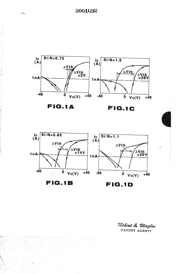
Figs. lA to lD show the VG-ID characteristic
(a relation of a drain current ID to gate voltae VG )
of a 2000 angstrom-thick gate insulating thin film
(SiN fllm) type transistor which is measured with a
varying Si/N composition ratio of the gate insulating
film 2.
Fig. lA shows the VG-ID characteristic at
Si/N = 0.75, an Si/N composition ratio of a gate insu-
lating film Si3N4 of a conventional thin film transis-
tor; Fig. ls the VG-ID characteristic at Si/N = 0.85;
Fig. lC the VG-VD characteristic at Si/N = 1.0 and
Fig. lD the VG-VD characteristic at Si/N = 1.1.
Figs. lA to lD show a variation of a drain current
ID (a source-to-drain channel current) measured against
that of a gate voltage VG in which case a drain voltage
VD is 10 V.
As appreciated from Figs. lA to lD, the thin film
transistor with the SiN film (Si:N = 0.75) used as the
gate insulating film has the VG-ID characteristic
revealing almost no hysteresis, that is, the size delta
Vth of the hysteresis is small.
.; '. ' ' . ,' ' ~ ~ , ' `' ,
. .: . ,, ~ .. .
. . ~ . . , . : -
:'::,''., . ' ~' ' :
9;~:
- 7 -
On the other hand, the thin film transistor for
memory which uses an SiN film (Si:N = 0.85 to 1.1) as
a gate insulating film has t:he VG-ID characteristic
which reveals a greater hyst:eresis as seen from Fig. lB
to lD, that is, the size delta vth of the hysteresis is
large.
In Figs. lA to lD, the size delta Vth of the hyst-
eresis is defined as a difference between a gate voltage
VG at ID = 1 nA at which the gate voltage VG gradually
varies from a negative value to +40 v and a gate yoltage
VG at ID = 1 nA at which the gate voltage VG gradually
varies from + 40 V to a negative value. In Figs. lA,
lB, lC and lD, delta Vth = 2 v, delta Vth = 14 v,
delta Vth = 28 V and delta Vth = 20 V, respectively.
The fact that the VG-ID characteristic has a
greater hysteresis size means that the thin fllm tran-
~ sistor has a memory function for storing charges in the
`~ gate insulating film. The thin film transistor with the
gate insulating film used as an SiN film whose Si/N com-
posltion ratio is 0.85 to 1.1 can be employed, as a mem-
ory device capable of a storing/releasing charges, by
controlling a voltage which is applied to the gate
electrode. The thin iilm transistor for memory holds
the effect of a voltage which is finally applied to the
gate electrode. That is, thin film transistor for
memory maintains storing state or releasiny state as far
as it does not receive any external electric effect. It
i92
-- 8
is thus possible to utilize the thin film transistor as
a memory device. The hysteresis size as set forth above
may also be called as a "hysteresis width~ or ~memory
width". The Si~ film (gate insulating film)~ though
being referred to as 2000 angstrom thick, may be within
a range 1500 angstrom to 4000 angstrom, desirably within
a range 2000 to 3000 angstrom (the thickness of a gate
insulating film of an ordinary thin film transistor),
provided that the aforementioned Si/N composition range
needs to be selected within a narrower range for a
thicker SiN film than the aforementioned SiN compo-
sition range Si/N = 0.85 to 1.1 to the aforementioned
2000 angstrom-thick SiN film.
It is considered that first data can be written
into the thin film transistor by applying a first volt-
age to the gate insulating film of that transistor whose
VG-ID characteristic is shown, for example, in Figs. lB
to lD, and second data different from the first data can
be written into the transistor by applying a second
voltage opposite in polarlty to the first electrode to
the gate insulating film of the transistor. The readout
of data which is stored in the thin film transistor can
be achieved utilizing the phenomenon that the level o~ a
current through a channel of the thin film transistor
varies depending upon a variation of voltage applied to
the gate insulating film.
By experiments conducted, the following are used as
.,~ ,
,. . . : .
:., : . .: ,
: :': ':.: ' ' :
, , " ..
" ' ' '' ''I, ~'~ , ', ', , ,
i9Z
g
the gate insulating film for imparting a memory function
to the thin film transistor:
(1) A silicon nitride film having an Si/N composi-
tion ratio ranging from 0.8ci to 1.1 and a thickness
ranging from 1000 to 3000 angstrom;
(2~ A multilayer film comprised of a silicon
nitride film having an Si~N composition ratio ranging
from 0.85 to 1.1 and an Si/N composition ratio ranging
from 0.7 to 0.8;
(3) A multilayer film having a silicon nitride
film and a high dielectric film;
(4) A multilayer film composed of an insulating
film and a semiconductor layer; and
(5) A silicon nitride film having a varying SiN
composition ratio in a thickness direction and an area
having an at least composition ratio of 1Ø
If the memory elements, comprised of such thin
transistors, are employed as a memory device, the thin
film transistors for memory are arranged as a matrix in
which case any memory element needs to be selectively
accessed. For that purpose, vari.ous transistors need to
be prepared, such as thin transistors for memory, thin
film transistors for selecting the memory element, and
those transistors for providing decoders and sense
amplifiers. As those transistors for a select purpose,
etc., transistors having VG-ID characteristics revealing
no hysteresis or a smaller hysteresis are employed.
. . .. : ...................... -
,. ~ , , , . ,;
. ~.. . :- . .
.: . . .. . .
:
-- 10 --
A memory element will now be explained below which
includes thin film transistors for memory having a VG-ID
characteristic revealing a hysteresis and thin film
transistors for select having a VG-ID characteristic
revealing no hysteresis.
As will be explained below, the term "a gate insu-
lating film having a hysteresis characterlstic" means a
gate insulating film which imparts the hysteresis to the
VG-ID characteristic of the thin film transistor. For
ease in distinguishing between the insulating film hav-
ing the hysteresis characteristic and that not having
any hysteresis characteristic, the latter insulating
film is indicated by dots in associated figures.
First Embodiment
Fig. 2 is a cross-sectional view showing a memory
element according to a first embodiment of the present
invention. The memory element of Fig. 2 comprises an
insulating substrate 11, a thin film transistor Tll for
memory which is formed over the insulating substrate 11,
and a thin film transistor T12 for select. The thin
film transistor Tll for memory comprises a gate elec-
trode Gll formed on a substrate 11, a gate insulating
film 12 formed on the gate electrode Gll and having a
hysteresis characteristic, a semiconductor layer 13
composed of an i (intrinsic)-a ~amorphous)-silicon
(polysilicon or single crystal silicon) formed over
the gate insulating film 12, an n+ (n type high
. -. , - .... ..
: , , : . ~ ,
, , :
;.
~;~, . ; . . " :
Z~ ;9Z
-- 11 --
: impurity)-a-silicon (polysil.icon or single crystal
silicon) contact layer 14 formed on the semiconductor
layer 13, and source electrode Sll and drain electrode
Dll both of which are formed on the contact layer 14.
s The thin film transistor T12 for select comprises
a gate electrode G12 formed on a gate insulatlng film 12
of the thin film transistor Tll, a gate lnsulating film
15 formed on the gate electrode G12 and having no
hysteresis characteristlc, an i-a-silicon tpolysilicon
lo or single crystal silicon) semiconductor layer 16 formed
on the gate insulating layer 15, an n+-a-silicon contact
layer 17 formed on the semiconductor layer 16, and a
source electrode S12 and drain electrode D12 whlch are
formed on the contact layer 16.
The thin film transistor T12 has i.ts source elec-
trode S12 connected by a wirlng layer 18 to the drain
electrode Dll in the thin film transistor Tll. A chan-
nel area of the thin film transistor Tll is covered with
a protective film 19 which has no hysteresis character-
istic. The gate insulating film 15 is etched away at an
area corresponding to a location of the thin film tran-
sistor Tll.
The thin film transistors Tll and T12 are covered
with a protective film 20 which is formed of SiN having
2s no hysteresis characteristic.
The method for manufacturing a memory element as
shown in Fig. 2 wlll be explained below.
. . . . , : "
: ' : , . ,
. ~ ~... . . .;
: ,
- 12 -
A metal film is formed on a substrate 11 and
pattern to form a gate electrode Gll. An insulating
film with a hysteresis characteristic is formed on the
resultant structure. The insulting film may be made of
a si~icon nitride film having a Si/N composition ratio
of 0.8 to 1.1 and a thickness of 1000 to 3000 angstrom.
An i-a-silicon (polysllicon or single crystal silicon)
film and an n+-a-silicon (polysilicon or single crystal
silicon) film are sequentially formed on the insulating
film. These films are patterned to form a semiconductor :
- layer 13 and contact layer 14. A metal film is formed
on the resultant structure and patterned to form a
source electrode Sll and drain electrode Dll. The con-
tact layer 14 is removed at an area situated over a
channel area. Then a protective film 19 is formed. It
is thus possible to form a thin film transistor Tll for
memory.
A metal layer is formed on the insulating film 12
and patterned to provide a gate electrode G12. An insu-
lating film with no hysteresis characteristic is formedon the resultant structure. The insulating film
may be made of, for example, a silicon nitride film hav-
ing an Si/N composition ratio of about 0.75. An i-a-
silicon film and an n~-a-silicon film are sequentially
formed on the insulating film. These two layers are
patterned to provide a semiconductor layer 16 and con-
tact layer 17. A metal film is formed on the resultant
:, ~ .. ,,. ,. : : :
:~. ~: ~ : , ,
~ : , . : .
,
. ~, .. .. . . .
,, ,. ~ .
.
- 13 -
structure and patterned to form a source electrode
S12 and drain electrode D12. The contact layer 17 is
removed at an area situated over a channel area. It is
thus possible to form a thin film transistor T12 for
select.
A metal lay~r is formed on the resultant structure
and patterned to provide a wiring layer 18. Then a pro-
tective film 20 is formed on the resultant structure.
In the first embodiment, the thin film transistors
Tll and T12 are formed at a separate step because the
gate insulating film 12 for the thin transistor Tll
needs to be formed to have a hysteresis characteristic
and becausa the insulating film 15 of the thin film
transistor 12 is formed to have no hysteresis
characteristic.
Second Embodiment
In the aforementioned first embodiment, the thin
transistors Tll and T12 are manufactured in the sepa-
rated step. A greater number of steps are thus required
in the manufacture of the transistors. In the first
embodiment, the thin film transistor T12 is formed on
the gate insulting film 12. For this reason, the -thin
film transistor T12 rises further than the thin film
transistor Tll, resulting in a wholly thickened memory
element structure.
The second embodiment is manufactured in less manu-
facturing steps and a memory element thus manufactured
. ;. . .
,: .
.- . .
9~
- 14 -
has a relatively thin structure as a whole.
The second embodiment will be explained below by
referring to Figs. 3A and 3B and 4A to 4D. Fig. 3A
shows a cross-section as taken along line A-A in
Fig. 3B. Fig. 3B shows main portlons so as to clarify
a positlonal relation among respective associated parts.
The structure of the memory element as shown in
- Figs. 3A and 3B will be explained below.
The memory element comprises an insulating sub-
lo strate 21 and a thin film transistor T21 for memory and
- thin film transistor T22 for select, both of which are
formed on the insulating substrate. Stated in more
detail, gate electrodes G21 and G22 are formed on the
- insulating substrate 21. A gate insulating film 22 is
formed on gate electrodes G21 and G22. Semiconductor
layers 23-1 and 23-2 of an i (intrinsic)-a (amorphous)-
silicon (single crystal or polysilicon) are formed on
the gate insuLating film 22 in a manner to oppositely
face the gate electrodes G21 and G22, respectively.
Contact layers 24-1 and 24-2 of n~ (n type high
concentration)-a-silicon (polysilicon or single crystal
silicon) are formed on the semiconductor layers 23-1 and
23-2, respectively. A source electrode S21 and drain
electrode D21 and a source electrode S22 and drain elec-
trode D22 are formed on the contact layers 24-1 and
2~-2, respectively. The drain electrode D21 of the thin
film transistor T21 and source electrode S22 of the thin
. ., ~ . . - .
.... . , , ~
:: . ~. . " ` ' , '' , , ' ,,
. ~ . . .
~16gX
~ - 15 -
.:
film transistor T22 are connected to each other by a
wiring layer 25. The source electrode S21 and drain
electrode D22 are connected to a source line SL and
drain line DL, respectively. The drain electrode D21 is
; 5 connected to the source electrode S22 through the wiring
layer 25. The thin film transistors T21 and T22 are
covered with a protective film 26 of a silicon nitride,
such as Si3N4, having no hysteresis characteristic.
; The gate insulatlng film 22 is shared by both the
thin film transistors T21 and T22 as a common insulating
film. The gate insulating film 22 is formed of an SiN
film having a hysteresis characteristic, such as an SiN
film whose Si/N composition ratio is 0.85 to 1.1.
`~ However, an area 22B of the gate insulating film 22
other than an area 22A for the thin film transistor T21
loses its hysteresis characteristic by an oxidizing or a
nitriding step.
In the memory element of the second embodiment, the
thin film transistors T21 and T22 share their gate insu-
lating film 22 as a common insulating film. Of the
insulating areas 22A and 22B of the insulating film 22,
the area 22A has the hysteresis characteristic and the
area 22B has no hysteresis characteristic. Thus the
thin film transistor T21 for memory has the VG-ID
characteristic revealing a hysteresis and the thin film
transistor T22 has the VG-ID characteristic having no
hysteresis.
:.. . . .. ~ ..
. -: .: - ,
. . . . :
. :- . " .
:,. . .
:.. : . .,: :
- 16 -
The manufacture of the memory element as shown in
igs. 3A and 3B will be explained below with reference
to Figs. 4A to 4D.
A conductive fllm such as a metal is formed on
an insulating substrate 21 to a thickness of about
1000 angstrom. The conductive film is patterned to pro-
vide gate electrodes G21 and G22. An SiN film is formed
by a plasma CVD method on the substrate 21. The CVD
step is performed by selecting an SiH4 (a main component
gaS)/NH3 flow ratio so as to form an SiN film whose com-
position ratio Si/N is 0.85 to 1.1. The gate insulating
~ilm 22 thus formed has a hysteresis characteristic. A
structure as shown in Fig. 4A is obtained by the afore-
mentioned steps.
The area 22A of the gate insulating film 22 corre-
sponding to the thin film transistor for memory is
masked with a resist mask 27. The exposed portion of
the gate insulating film 22 is oxidized or nitrided by,
for example, a plasma oxidation method or a plasma
nitriding method. By the oxidation method, the area 22
of the gate insulating film 22 has a composition SiON,
losing its hysteresis characteristic. By the nitriding
method, the area 22B of the gate insulating film 22 has
a smaller Si~N composition ratio and loses its hyste-
resis characteristic. A structure as shown in Fig. 4Bis obtained by the aforementioned steps.
A resist mask 27 is removed from the resultant
- . .... . .. ~ -~ , , -
,: .; . . ,
.. : : . :
-. . . "
.
: :: '
~: ,
-- 17 --
:
structure. An i-a-silicon (single crystal or poly-
silicon) film and n~~-a-silicon (single crystal or
polysilicon) film are sequentially formed on the gate
insulating film 22 and patterned to provide semicon-
ductor layers 23-l and 23-2 and contact layers 2~-1 and
24-2. A metal fllm is deposited by, for example, an
evaporation or a sputtering method on the resultant
structure and patterned to provide source electrodes S21
and S22 and drain electrodes D21 and D22. Those areas
of the contact layers 2~-l and 24-2 situated over chan-
nel areas are removed from the resultant structure. By
these steps it is possible to obtain a thin film tran-
sistor T21 for memory and thin film transistor T22 for
select, as shown in Fig. ~C.
A metal film is formed on the resultant structure
and patterned to provide a source line SL, drain line DL
and wiring layer 25, as shown in Fig. 4D. A protective
film 26 of SiN having no hysteresis characteristic is
formed on the resultant structure to provide a memory
element as shown in Fig. 3.
In the formation of the source electrodes S21 and
S22 and drain electrodes D21 and D22, the wiring layer
25 may also be formed of the aforemetioned metal film.
In the memory element of the second embodiment, the
transistors T21 and T22 share their gate insulting film
22 as a common insulating film. Thus the layer struc-
ture of the second embodiment can be made thinner than
.,~,... . .
.~, . . . .
' ~;~" " '' ' ' '
~ ' , .' ~' ' ~
2~ i9;~
- 18 -
'
that of the first embodlment. The structure of this
memory element can ensure the formation of both the
transistors by substantially the same manufacturing
steps.
In the manufacture of the memory element o~ the
second embodiment, an SlN film 22 havlng a hysteresis
characteristic is formed, and then, the hysteresis
` characteristic of a select-transistor formation area of ?
the gate insulating film 22 is removed. The gate elec-
trodes G21 and G22, semiconductor layers 23-1 and 23-2,
contact layers 24-1 and 24-2, and electrodes S21, S22,
D21, D22 are formed in that order at the respective
steps. It is thus possible to substantially simultane-
- ously form the transistors T21 and T22.
In the structure shown in Fig. 3A, the transistors
T21 and T22 are of an inverted stagger type, but may
be of a stagger, an inverted coplanar or a coplanar
type. Figs. 5, 6 and 7 show memory structures comprise
stagger type thin film transistors, that of inverted
coplanar type thin film transistoris and that of coplanar
type thin film transistors, reispectively. In these
Figures, identical reference numerals are employed to
designate similar part or portion throughout.
Therefore, any further explanation is omitted.
Even in Figs. 5, 6 and 7, a thin film transistor
for memory and thin film transistor for select share a
gate insulating film 22 as a common insulating film in
~ 16g2
- 19 -
which case the hysteresis characteristic of a gate insu-
lating film 22B is removed ~rom the corresponding area
of the gate insulating film 22. Even in this embodi-
ment, it is possible to mamlfacture a memory element of
a thin structure in less manu~acturing s-teps.
The memory element shown in Fig. 5 can be manufac-
tured by forming source and drain electrodes, a contact
layer and semiconductor layer, gate insulating film, and
gate electrode in that order.
lo The memory element shown in Fig. 6 can be manufac-
tured by forming a gate electrode, gate insulating film,
source and drain electrodes, contact layer and semicon-
ductor layer in that order.
The memory element shown in ~ig. 7 can be manufac-
tured by forming a semiconductor layer, contact layer,source and drain electrodes, gate insulating film and
gate electrode in that order.
Third Embodiment
-
A third embodiment of the present invention will be
explained below by referrlng to Figs. 8 and 9A to 9C.
A memory element of a third embodiment will be
explained below with reference to Pig. 8. As shown in
Fig. 8, a gate electrode G31 for a thin film transistor
T32 for memory and gate electrode G32 for a thln film
transistor for select are formed on an insulating
substrate 31 such as glass. A gate insulating film 32
is formed on the gate electrodes G31 and G32 and on the
.
. . .
~'' :, ' . ' ,
:...
.. ~ : . ,
~`. ~ ' '
:' ;
9;~
- 20 -
surface of the substrate. On the gate insulating film
32, semiconductor layers 33-1 and 33-2 of i-a-silicon
are formed in a manner to oppositely face gate elec-
trodes G31 and G32, respectively. Contact layers 34-1
and 34-2 of n+-a-silicon are formed on the semiconductor
layers 33-1 and 33-2, respectively. A source electrode
S31 and drain electrode D31 and a source electrode D32
and drain electrode D32 are formed on the contact layers
34-1 and 34-2, respectively. The thin film transistor
T21 for memory is connected by a wiring layer 35 to the
thin film transistor T32 for select.
The basic structure shown in Fig. 8 is the same as
that shown in Fig. 3A. However, the gate insulating
film 32 is different from the gate insulating film 22,
because the film 32 is formed of an SiN film having no
hysteresis characteristic. The gate insulating film 32
is formed of an SiN film whose Si/N composition ratio is
made substantially equal in value to a stoichiometric
ratio (Si/N = 0.75). A silicon ion is implanted into a
thin film transistor for memory formation area of the
gate insulating film 32 to make the value of Si/N
ratio greater than that of the stoichiometric ratio
in which case Si/N = 0.~5 to 1.1. Thus the gate insu-
lating film ~2 has an area 32A having a hysteresis
characteristic and an area 32B havlng no hysteresis
characteristic.
The manufacture of the memory element of the third
~.,~ ... .. .
., . - , ; , . .
.
. ~ . .
. . .
692
- 21 -
embodiment will be explained below with respect to
Figs. 9A to 9C.
A metal film is formed on an insulating substrate
31 and patterned to form gate electrodes G31 and G32.
An SiN film 32 is formed by, for example, a plasma CVD
method on the resultant structure. The CVD step is car-
, ried out so -that the Si/N composition ratio of the SiN
film 32 may be nearly 0.75. A semiconductor layer 33
and n+-a-silicon layer 3~ are sequentially formed on the
SiN film 32 by means of, for example~ the plasma CVD.
If the SiN film 32 and semiconductor layer 33 are sequ-
entially formed in a high vacuum atmosphere, provide a
better i-a-Si to SiN interface. It is thus possible to
obtain thin film transistors Tl and T2 having a stable
characteristic.
A resist mask 36 is formed over the n+-a-silicon
layer 34 and has an opening over the memory element area
32A. rhrough the opening, Si ~ons (Si+) are implanted
into an area 32A of the ga'e insulating film 32. The
ion implantation step is conducted by controlling accel-
eration voltage so that the peak of an Si-ion range is
located within the gate insulating film 32. The dose of
the ion is set such that the Si/N composition ratio of
the area 32s is nearly 0.8 to l.1. By doing so, a
hysteresis characteristic is imparted to the area 32A
enough adequate to allow the thin film transistor T31 to
perform a memory function. The structure as shown in
,;,,~.. ., . , , , , ....................... : ~ ,
,
: : : ::: . . . . . . . ' . . . .
", , : : ;
~0~69~
~2 -
Fig. 9B can be obtained by carrying out the aforemen-
tioned steps.
The resist mask 36 is removed from the resultant
structure. The n~-a-silicon layer 34 and semicon-
ductor layer 33 are patterned to provide semiconductor
. .
layers 33-1 and 33-2 and contact layers 3~-1 and
34-2.
A metal film is deposited on the resultant struc-
~` ture and patterned to provide source electrodes S31 and
S32 and drain electrodes D31 and D32. The portions of
the contact layers 34-1 and 34-2 situated over the chan-
- nel areas are etched away by the etching step.The memory element as shown in Fig. 8 is completed
by the aforementioned steps.
lS The thin film transistors T31 and T32 in the third
embodiment share their gate insulting film 32 as a com-
mon insulting film. The memory element of the third
embodiment, like that of the second embodiment, can be
made thinner as a whole than that of the first embodi-
ment. It is possible to manufacture the thin film tran- ;
sistors for memory and select by substantially the same
steps. According to the third embodiment, the thin film
transistors T31 and T32 can be efficiently manufactured
in less manufacturing steps than those of the first
embodiment.
In the third embodiment, subsequent to forming the
semiconductor layer 33 and contact layer 34, Si ions are
.. :, . . ~ . . .
.. . . .
..... .. . . .
,: ~ : .
.,.; , .
i9~
- 23 -
:
implanted into the memory device formation area 32A of
the gate insulating film 32. It may be possible to,
subsequent to forming a gate insulating film 32, that
is, prior to forming the gate insulating film 32,
implant silicon ions into the area 32A.
Although, in the third embodiment, the thin film
transistors T31 and T32 are made of an inverted stagger
type, they may be of a stagger, coplanar and inverted
coplanar type. In these types, the thin film transis-
tors Tl and T2 can simultaneously be formed if theirtransistors is so ~ormed as to share the gate insulating
film as a common insulating film. The memory element
composed of staggered type thin film transistors can be
fabricated by forming source and drain electrodes, a
contact layer and a semiconductor layer, a gate insulat-
ing film and a gate electrode in that order. The memory
element composed of coplanar type thin film transistors
can be manufactured by forming a semiconductor layer and
a contact layer, source and drain electrodes, a gate
insulating film and a gate electrode. The memory ele-
ment composed of inverted coplanar type thin ~ilm
transistors can be fabricated by forming a gate
electrode, a gate insulating layer, source and drain
electrodes, a contact layer and semiconductor layer in
that order.
~ourth Embodiment
A fourth embodiment of the present invention will
- : ,
' :; ~: , : : : - . '
,: - . .
: . : .~ :
~ :: . . ~
.,' ~ . - ' ' -, ' ~ ' ,..... ' ..... .
~ - 24 -
.' .
be explained below by referring to Figs. 10 and llA to
- :~
llD.
A memory element of the fourth embodiment will be
explained below with rsference to Fig. 10.
Gate electrodes G41 and G42 of thin film
. transistors T41 for memory and T42 for select, are
`, formed on an insulating substrate 41. A high breakdown
voltage dielectric layer 42 composed of TaOx (tantalum
oxide) is formed on the substrate and gate electrodes
G41 and G42. A gate insulating film 43 composed of SiN
is formed on the dielectric layer 42. An intrinsic sil-
icon semiconductor layer 44-1 is formed on a thin film
transistor T41 for memory formation area of the gate
insulating film 43 in a manner to be located opposite to
the gate electrode G41. An intrinsic silicon semicon-
ductor layer 44-2 is formed on a thin film transistor
T41 for select formation area of the gate insulating
film 44-2. A source electrode S~l and drain electrode
D41 and source electrode S42 and drain electrode D42 are
formed on the semiconductor layers 44-1 and 4~-2,
respectively. The drain electrode D41 of the thin film
transistor T41 for memory is connected by a wiring
layer, not shown, to the source electrode S42 of the
thin film transistor T~2 for select. The thin film
transistors T41 and T~2 are covered with a protective
film 45.
The gate insulating film 43 is shared by the thin
: .; . . : ~ ,. .
,-; - , : . ~: ~ : '
..... . . .
~t 10~692
- 2s -
film transistors T41 and T42 as a common insulating
film. The gate insulating film 43 is so formed that its
area corresponding to the transistor T41 is thinner than
the other area corresponding to the transistor T42.
Stated in more detail, the gate insulating film 43 com-
prises a first SiN film 43A formed relative to the thin
film transistor T41 for select and second SiN film 43s
formed relative to the transistor 41 and the transistor
T42. The gate insulating film of the transistor T41 for
; 10 memory is formed of the second SiN film 43B, and the
gate insulting film of the transistor T42 for select is
formed of a doublelayer structure composed of the first
SiN film 43A and second SiN film 43B. The first and
second SiN films 43A and 43B are made of the same mate-
rial whose Si/N composition ratio is made substantially ;
equal in value to a stoichiometric ratio in which case
Si/N = 0.75. The first SiN film 43A and second SiN film
43s are about 2000 angstrom and about 500 angstrom,
respectively. That is, the gate insulating films of the
thin film transistors Tl and T2 are about 500 angstrom
and about 2500 angstrom, respectively.
The thin film transistor T41 for memory has a thin-
ner gate insulating film which has no adequate breakdown
voltage characteristic. The breakdown voltage of the
gate insulting film 43 is compensated by the high break-
down voltage layer 42. Ta2O5 is ideal as a TaOx consti-
tuting the dielectric layer 42. The dielectric layer 42
;:' . , : .
... ~, ., . ~ , ' ; ;: , .
,
9;~
- 26 -
~ is about 2000 angstrom thick.
- The hysteresis characteristic of the thin film will
be explained below. Fig. 12 shows the VG-ID character-
istic of the thin film transistor. As the thin film
transistor for memory it is necessary that it have a
greater delta V-th. As the thin film transistor for
select, there is a need for a transistor whose delta Vth
is nearly "zero". The delta Vth of the thin film tran-
sistor is determined by the intensity of an electric
field applied to the gate insulating film. Fig. 1~
shows a relation of the intensity of an electric field
in the gate insulating film (voltage per unit thickness)
v/cm to delta Vth of the thin film transistor. As shown
in Fig. 13, an increase in the intensity of an electric
field leads to a rise in delta Vth. Fig. 14 shows a
relation of the thickness of the gate insulating film to
the intensity of an electric field, V/cm. As will be
seen from Fig. 14, the intensity of the gate insulating
film is in inverse proportion to the thickness of the
gate insulating film. For a 2000 angstrom-thick Ta2O5
to be used as a dielectric material, the intensity o~
the electric field in the gate insulating film whose
Si/N composition ratio is 0.75 is as small as El =
1 MV/cm for the film thickness of 2500 angstrom and as
large as E2 = 3 MV~cm for the film thickness of
500 angstrom.
As appreciated from the above, even if the same
~........ .
,.. ~ - .: , , . :
:
:' '' . ' ' ' '
,. . .
;9~
- 27 -
material is used for the gate insulating film, the
intensity of an electric field which governs the VG-ID
characteristic of the thin film transistor can be varied
by the thickness of the gate insulating film. The
aforementioned intensity of the electric field is in
inverse proportion to the thickness of the gate insula-
tion film. Therefore, as shown in Fig. 10, the use of
a different thickness for the gate insulating film of
the transistor for memory and transistor for select can
impart the VG-ID characterlstic revealing almost no
hysteresis curve to the transistor T42 for select and
the VG-ID characteristic revealing an adequate hyste-
resis to the transistor T41 for memory.
The method for manufacturing a mernory element will
be explained below by referring to Figs. llA to llD.
~ A metal film is formed on an insulating substrate
41 and patterned to substantially simultaneously form
gate electrodes G41 and G42. An about 2000 angstrom-
thick TaOx (desirably Ta2O5) is deposited by the plasma
CVD method on the insulating substrate to provide a high
breakdown voltage dielectric layer 42. Silicon nitride
is deposited by the plasma CVD method on the dielectric
layer ~2 to a thickness of about 2000 angstrom to form a
first SiN f:Llm ~3A. The CVD step ls conducted by
selecting an SiH4 to NH3 flow ratio so that the Si/N
value of the SiN film formed is nearly 0.75. A struc-
ture as shown in Fig. llA is obtained by these steps.
:, ~ , . ~ . ,, : ,
~,
, . . , . .:
' :, . .
. , '
9z
; - 28 -
,`, . ,
A portion of the flrst SiN fllm 43a correspondlng
to the device area of the transistor T41 is cut away to
expose a high breakdown voll,age dielectric layer 42.
The first SiN film 43A is left at a transistor T42 for-
mation area. A structure as shown in Fig. llB isobtained by the aforementioned steps.
.~
An about 500 angstrom-thick SiN is deposited by
. plasma CVD method on the first SiN film 43A and exposed
high breakdown voltage dielectric layer 42. This CVD
steps are performed under the same condition as that
under which the formation of the first SiN film 43A is
done. A gate insulating film 43 comprising the first
SiN film 43A and second SiN film 43B is shared by the
thin film transistors T42 and T41 as a common insulating
film. A structure as shown in Fig. llC is obtained by
the aforementioned step.
An intrinsic silicon is formed by the plasma CVD
method on the gate insulating film 43 and patterned to
simultaneously form semiconductor layers 44-l and 44-2.
~ A metal layer is formed on the resultant structure and
patterned to provide source electrodes S41 and S42,
drain electrodes D41 and D42 and a wiring layer connect-
ing the source electrode S42 to the drain electrode D41.
A structure as shown in Fig. llD is obtained by the
25~ aforementioned step.
A protective insulating film 45 is formed on the
` resultant structure, completing a memory element as
:
. . . . .
g~
- 29 -
shown in Fig. 10.
~ According to the fourth embodiment, a memory ele-`~ ment structure can be manufactured, as a ~hinner unit,
in less manufacturing steps in comparison with the
-~ 5 case of the first embodiment. In the method for manu-facturing a memory element of the fourth embodiment
it is possible to substantially simultaneously form
transistors T42 and T41 easily in the simpler steps.
The Si/N composition ratio o~ the gate insulating
film 43 is not restricted to a value of its stoichiomet-
ric ratio, Si/N = 0.75. It is possible to, for example,
make the Si/N composition ratio of the gate insulating
film greater than 0.75. In this case, the gate insulat-
ing film of the element area of the transistor T41 and
that of the transistor T42 are formed such that they are
thicker than that of the gate insulating film of the
aforementioned embodiment.
The high breakdown voltage dlelectric layer 42 for
compensating for the breakdown voltage of the gate insu-
lating film may be formed at a thinner area alone of the
gate insulating film 43, that is, the portion of the
transistor T41. If the breakdown voltage of the gate
insulating film can be ensured, it is not necessary to
provide the high breakdown voltage dielectric layer 42.
In the aforementioned embodiment, the transistors
T41 and T42 are of an inverted stayger type. 30th the
transistors may be of a stagger, a coplanar and
.,
: .. ,: . .: . . .. .
, . .
:,. , ~ -:: : ,: . .
.. : :.. : ' ,, , ' :
~ .
9z
- 30 -
; an inverted coplanar type.
A memory element composed of stagger thin film
transistors is fabricated by forming source and drain
electrodes, a semiconductor layer, a gate insulating
film, a high breakdown voltage dielectric layer and a
gate electrode in that order. A memory element composed
of coplanar type thin film transistors is manufactured
by forming a semiconductor layer, source and drain
electrodes, a gate insulating film, a high breakdown
voltage dielectric layer and a gate electrode in that
. .
order. A memory element composed of inverted coplanar
type thin film transistors is manufactured by forming a
gate electrode, a high breakdown voltage dielectric
layer, a gate insulating film, source and drain elec-
trodes and semiconductor layer in that order.
The first and second SiN films 43A and 43B can beformed in that order or in reverse order.
In the aforementioned embodiment, the gate insulat-
ing film for the thin film transistor T~2 for select is
formed as a doublelayer structure. The gate insulating
film ~3 may wholly be formed as a single layer in which
case an area for the thin film transistor T~l is made
thinner by a half etching step than the rest af the gate
insulating film.
Fifth Embodiment
A memory element according to a fifth embodiment
of the present invention will be explained below by
~:.,
., ~ . . - ~
.: :; .: . .
, ,,.. .:,
- 31 -
referrlng to Fig. 15 and 16A to 16E.
Fig. 15 is a cross-sec:tional view showing a memory
element according to a fifth embodiment of the present
invention. The memory element comprises an insulating
substrate 51 such as glass and a thin ~ilm transistor
T51 for memory and thin film transistor T52 for select,
both of which are formed on the insulating substrate.
The thin film transistor T51 comprises a gate elec-
trode G51 formed on a su~strate 51, a gate insulating
film 52 of SiN which is formed on the gate electrode
G51, a semiconductor layer 53 of i-a-silicon which is
formed on the gate insulating film 52, a contact layer
; 54 of n+-a-silicon which is formed on the semiconductor
layer 53, and source and drain electrodes S51 and D51.
The gate insulating film 52 has a charge storage func-
tion and an Si/N composition ratio (Si/N = 0.85 to 1.15
greater than its stoichiometric ratio (Si/N = 0.75).
The thln film transistor T52 for select comprises a
gate electrode G52 formed on the substrate 51, a gate
insulating film 55 of SiN which is formed on the gate
electrode G52, a semiconductor layer 56 of i-a-silicon
which is formed on the gate insulating film 55, a semi-
conductor layer 56 of i-a-silicon formed on the gate
insulating film 55, a contact layer 57 of n+-a-silicon
which is ~ormed on the semiconductor layer 57, and
source and drain electrodes S52 and D52. The gate insu-
lating film 55 has an Si/N composition ratio equal to
~, . ., ~ . . . . .
,: ' ~. ', . , '' ' ~
:,; , . . : :
, . . ~ , . , , . , :
:' ':, . . .
.. .. . .
.. : ; ,, . , ~' . .. ~,,
9~
- 32 -
the stoichiometric ratio (Si/N = 0.75) and has no charge
storage function.
The drain electrode D51 of the thin film transistor
T51 is connected by a wiring layer, not shown, to the
source electrode S52 of the thin film transistor T52.
The thin film transistors T51 and T52 are covered with a
protective film 59.
The method of manufacturing the memory element
according to the present invention will be explained
below by referring to Figs. 16A to 16E.
A metal film, such as chromium, is formed by a vac-
uum evaporation or sputtering method on an i~sulating
substrate 51 to a thickness of 1000 angstrom and pat- ~-
terned to provide gate electrodes G51 and G52 and a
gate wiring, not shown, connecting the gate electrode
G51 to the gate electrode G52. A structure as shown in
Fig. 16A is obtained by the aforementioned manufacturing
steps.
An insulating film of silicon nitride with an
Si/N composition ratio substantially equal to its
stoichiometric ratio (Si/N = 0.75), an i-a-silicon
layer, an n+-a-silicon layer and metal film, such as
chromium, are sequentially formed by, for example, a
plasma CVD, vacuum evaporation or sputtering method on
the substrate to a thickness of 3000 angstrom,
1500 angstrom, 250 angstrom and 500 angstrom, respec-
tively. The each layer and film is patterned by
, .. . . . . . . . .
:: ~ .. .. ... . .. . . . .
:-: . - :., . , : .
:,~.,, , .. ' ',, ~
~,
:.. ~: . . .
: : ... - . . . :
~. . .
: , . .
, ~ . :
;:; . .:. : . :
.: :
.
;92
- 33 ~
a photolithographlc method, leaving a transistor T42
(transistor for select) formation area alone. A struc-
ture as shown in Fig. 16B is obtained by the a~oremen-
tioned steps.
A silicon nitride layer whose Si/N composition
ratio is 0.85 to 1.15, an i-a-silicon layer, an n+-a-
silicon layer and a metal film are formed by a plasma
CVD, vacuum evaporation or sputtering method on the
- resultant structure to a thickness o~ 2000 angstrom,
1500 angstrom, 250 angstrom and 500 angstrom, respec-
? tively. The each film and layer is patterned by a
photolithographic method, leaving a transistor T41
(transistor for memory) formation area alone. A struc-
ture as shown in Fig. 16C is obtained by the a~oremen-
~! 15 tioned steps.
Metal films 58, 59 and n+ type semiconductor layers
54, 57 are patterned by the lithographic method to pro-
vide source electrodes S51, S52 and drain electrodes
D51, D52, the source wiring layer connected to the
source electrode S51 and the drain wiring layer con-
nected to the drain electrode S52. The n+ type semicon-
ductor layers 54, 57 are removed at other than those
areas which are situated below the electrodes S51, ~51,
S52, D52 and wiring layer. A structure as shown in ?
Fig. 16D iS obtained by the aforementioned steps.
Then the semiconductor layers 53 and 56 are pat-
terned by the photolithographic method to a transistor
':': . . . . .. .
' : :' ' ' ' : , . `
.: ' ' ~:,
: ' ',
:::: ': .. : ' .
ZO~lG92
- 34 -
., :
element pattern. The thln film transistors T51 and T52
as shown in Fig. 16E are thus completed by the aforemen-
tioned steps.
The wiring layer connecting the electrode D51 and
` 5 the source electrode S52 is formed. Then a protective
insulating film is formed on the resultant structure. A
structure as shown in Fig. 15 iS completed.
A multilayer structure comprising the gate insulat-
ing film 55, semiconductor layer 56, contact layer 57
10 and metal film 59 and a multilayer structure comprising
the gate insulating film 52, semiconductor layer 53,
contact layer 54 and metal film 58 are formed in that
order and in reverse order.
In the method for manufacturing the memory element,
. 15 a plurality of components are formed by a single pat~
terning step. It is thus possible to manufacture such
dev~ces efficiently in less patterning steps.
The gate insulating film 52 having a charge storage
function may be formed as a doublelayer structure such
that a 1000 to 5000 angstrom-thick high dielectric film
having a dielectric constant of bout 10 is formed on
the gate electrode G51 and that a 50 angstrom to
2000 angstrom-thick silicon nitride film whose Si/N com-
position ratio is about 0. 75 iS formed on the semicon-
ductor layer 53. The gate insulating film of such a
doublelayer structure has an adequate charge function.
Furthermore, the gate insulating film 52 may be of such
: ~: ~. - . ~ . : . : : , :
, ., ,: :
;9z
- 35 -
a type that it has a charge storage function, that is, a
hysteresis characterlstlc.
Although, ln the aforementloned embodiment, the
; memory element has been explained as connecting the thin
film transistor T51 to the thin film transistor T52, the
present invention can also be applied to a memory ele-
- ment of such a type that a llne select thin film tran-
sistor is connected to the wiring layers for the gate,
source and draln electrode of the thln film transistor
for memory so as to select these wiring layers.
Sixth Embodim nt
A memory element according to a sixth embodiment of
~ the present invention will be explained below by refer-
; ring to Figs. 17 and 18A to 18D.
A memory element of this embodiment will be
explained below with reference to Fig. 17.
Ir~ Fig. 17, a gate electrode G61 for a thin film
transistor T61 for memory and gate electrode G62 for a
thin film transistor T62 ~or select are formed on an
insulating substrate 61. A gate insulating film 62 is
formed on the gate electrodes G61 and G62. Semiconduc-
tor layers 63-1 and 63-2 of i-a-silicon are formed on
the gate insulating film 62 in a manner to be situated
opposite to the gate electrodes G61 and G62, respective-
ly. Contact layers 64-1 and 6~-2 of n+-a-silicon are
formed on the semiconductor layers 63-1 and 63-2,
respectively. A source electrode S61 and drain
.. ~:: .. ' .' ' ' , . : ' ' ` , '
'': : ' ' ........................ `
.. . . : ` .
169~
- 36 -
electrode D61 and a source electrode S62 and drain elec-
trode D62 are formed on the contact layers 6~-1 and
64-2. The drain electrode D61 for the thin film tran-
sistor T61 for memory and the source electrode S62 of
the thin film transistor for select are connected to
each other via a wiring layer 65 which is formed inte-
gral with both the electrodes D61 and S62. A source
electrode S61 iS connected to a source line SL integral
therewith. The drain electrode D62 is connected to a
~ 10 drain line DL integral therewith~ The wiring layer 65
`' and source line SL and drain line DL are formed on the
gate insulating film 62. The gate electrode G61 and the
gate electrode G62 are connected to a gate line not
shown. The thin film transistors T61 and T62 are
covered with a protective film 65.
The gate insulating film 62 comprises an insulating
film 62A situated at element areas of the transistors
T61 and T62 and a thin insulating film 6~B situated
between the gate electrode G62 and the gate insulating
film 62A and having no hysteresis characteristic. The
gate insulating film 62A iS formed of silicon nitride
having a hysteresis curve, such as silicon nitride whose
Si/N composition ratio 0.85 to 1.15. The gate insulat-
ing film 62B is formed of silicon nitride or silicon
o~ide having no hysteresis, such as silicon nitride
whose Si/N composition ratio is substantially equal to
its stoichimetric ratio (Si/N = 0.75).
:. :: ;, ., .:
. ~ , . . . . . .
69~
- 37 -
Since the gate insulating film 62~ has a hysteresis
characteristic in the present memory element, the thin
; film transistor T61 can be employed as a memory device.
The thin film transistor T62 has its hysteresis
` 5 characteristic diminished by the gate insulating film
62B. The size of the hysteresis of the transistor T62
varies depending upon the thickness of the gate insulat-
ing film 62B. If the gate insulating film 62B is formed
with a thickness with which the transistor T62 loses its
hysteresis characteristic, a thin film transistor T62
can be formed having a better switching characteristic,
not a hysteresis characteristic. Since the transistors
T61 and T62 share their gate insulating ~ilm 62 as
a common insulating film, it is possible to impart a
desired function to the transistors T61 and T62.
The method for manu~acturing a memory element will
be explained below with respect to Figs. 18A to 18D.
A metal film, such as chromiurn, is deposited on
an insulating substrate 61 and patterned to form gate
electrodes G61, G62 and a gate line for connecting the
gate electrode G61 to the gate electrode G62. A struc-
ture as shown in Fig. 18A is formed by these steps.
Silicon nitride whose Si/N composition ratio is
substantially equal to its stoichiometric ratio (Si/N =
0.75) is deposited by the plasma CVD method on the
insulating substrate 61 and patterned by the photo-
- lithographic method to provide a silicon nitride
,. . ~ , . , ; . . . ;
.
: . -, . . . . .
.~ . . . . . . . .
. . . . ..
~-:, . . .. .
9~
~ - 38 -
:~`
film 62B on the gate electrode G62 as shown in Flg. 18B.
Silicon nitride whose Si/N composition ratio is
0.85 to 1.15 is deposited by the plasma CVD method on
the resultant structure to form a gate insulating film
62A. An i-a-silicon layer and n+-a-silicon layer are
sequentially formed by the plasma CVD method and pat-
terned to provide semiconductor layers 63-1 and 63-2 and
contact layers 64-1 and 64-2. A structure as shown in
Fig. 18C is formed by these steps.
A rnetal film ls deposited on the resultant struc-
ture and patterned to simultaneously form a source elec-
trode S61 and drain electrode D61, a source electrode
S62 and drain electrode D62, a wiring layer 65, a source
line SL and drain electrode DL as shown in Fig. 18D.
The contact layers 64-1 and 64-2 are etched away at an
area which is situated over the channel area. By these
steps, a thin film transistor T61 for memory and thin
film transistor T62 for select are formed as shown in
Fig. 1 8D .
An overlying protective film 67 is formed on the
resultant structure to form the memory element as shown
in Fig. 17.
In accordance with this embodiment, it is possible
to substantially simultaneously form transistors T61 and
T62 and hence to form the memory element efficiently in
less manufacturing steps. Since the transistors T61
and T62 share their gate insulating film as a common
. ..... .. . . . . .
, , , . . i
692
- 39 -
,
insulating film, this memory element can wholly be made
thinner than the memory element of the first embodiment.
The thin film transist:ors T61 and T62 can be formed
substantially simultaneousl.y in accordance with the
- 5 aforementioned manufacturing method.
The wiring layer 65, source line SL and drain line
DL in one group and a source electrode S61 and drain
electrode D61 and source electrode S62 and drain elec-
: trode D62 in another group may be formed in a separate
step.
lthough, in the aforementioned embodiment, the
thin film transistors have been explained as being of
an inverted stagger type, they may be mad0 a stagger
type, a coplanar type or an inverted coplanar type.
Even i.n this case, a thin film transistor for memory
and khin film transistor for select share their gate
. insulating film as a common insulating film in which
case the insulating film comprises an insulating film
having a hysteresis characteristic and an insulating
film formed on a gate electrode of the thin fllm tran-
sistor for select and having no hysteresis character-
istic.
A memory element composed of stagger type thin
film transistors can be fabricated by forming source and
drain electrodes, a contact layer and a semiconductor
layer, a gate insulating film having a hysteresis
characteristiF, a gate insulating film having no
,. ~
z
~ ~o -
hysteresis characteristic, and a gate electrode. A
memory element composed of coplanar type thin film tran-
sistors is manufactured by forming a semiconductor layer
and a contact layer, source and drain electrodes, a gate
insulating film having a hysteresis characteristic, a
gate insulating film having no hysteresis character-
istic, and a gate electrode in that order. A memory
element composed of inverted coplanar type thin film
transistors is fabricated by forming a gate electrode, a
gate insulating film having no hysteresis character-
istic, a gate insulating film having a hysteresis
characteristic, source and drain electrodes, a contact
layer and a semiconductor layer in that order.
Although the sixth embodiment of the present
invention has been explained in connection with the
memory element having the thin film transistors T61 and
T62 connected to each other, the present invention is
not restricted to that emhodiment. For example, the
present invention can be applied to the memory element
having a select thin film transistor so as to select
lines connected to the gate, source and drain electrodes
of the thin film transistor for memory.
As set forth above, according to the present
invention, a thin film transistor having a memory func-
2S tion and ordinary switching thin film transistor can beformed at one substrate.
The arrangement and operation of a memory circuit
: , . i : :
: ' '. ,~ . .. . .
32
- 41 -
using memory element as set: forth above will be
explained below with reference to Fig. 19. The opera-
tion of this memory circult: differs the operation of
general E2PROM.
In the arrangement shown in Fig. 19, a transistor
TM for an memory element has its current path connected
in series with that of a transistor TS for select to
form a pair of transistors. The transistor TM has a
hysteresis characteristic and the select transistor TS
- 10 has no hysteresis characteristic and is of such a
switching type that it is turned ON when a voltage whose
`, absolute value is greater than a predetermined level(~or example ~10 V or more or -10 V or less) is applied
;~ to the gate electrode of the select transistor TS. Such
pairs of transistors TM, TS are connected in a matrix
array. The gate line ~word line) GL of transistors TM
and TS on the same row is commonly connected to the
gates of the transistors TM and TS. A drain line DL
is commonly connected to the current path of each
select transistor TS on the same column. One end of the
current path of each memory transistor TM on the same
column is connected to a source line (bit line) SL.
The gate line GL is connected to a row decoder RD
and drain lines DL and source lines SL are commonly con-
nected to a column decoder CD. The source lines SL are
commonly connected to a sense amplifier SA. A reference ! "
voltage generator RG is connected to the sense amplifier
''`, ~''~f . ' ' ' ,; ' . ; . " ' . ' ., ,, " ' ' . . ' ' , ' ' '. ~ ' ' ' ' . "
~', i ' ' ~, ' ' ' ~ ' '
'',,~' ','' ' " ' " '
692
- 42 -
SA. A row address, write c:ontrol signal, read control
and erase instructlon signal are connected to the row
decoder CD. A column address, wrlte control signal,
read control signal and erase instruction signal are
connected to the column decoder CD.
The row decoder RD, column decoder CL and sense
amplifier SA are composed of thin ~ilm transistors hav-
ing no hysteresis characteristic.
A) Writing data (logic 1) into the memory element
in the arrangement shown in Fig. 19 will be explained
below.
; The row and column addresses of the memory transis-
tor TM to be accessed are supplied to the row decoder
RD and column decoder CD with a write signal set at
an active level. The row decoder RD is responsive to an
input signal to set a voltage on a gate line GL of a
corresponding row to, for example, vp/2 in which case
voltages on the other lines are set to, for example,
0 V. If, for example, the gate voltage can vary in a
range from +40 V to -40 v, then Vp/2 is set to, for
example, 20 v. The column decoder CD is responsive to
an input signal to set a voltage on the drain and source
lines DL and SL on the corresponding column to, for
example, -vp~2 (-20 V) in which case the other lines are
set to, for example, 0 V. The select transistor TS is
responsive to a corresponding gate voltage to turn the
select transistor TS ON, allowing the -vp/2 to be
; ~.... .. . .
:., ;~ ,. : . , . :
,. . . . .
92
- 43 -
applied to the source and drain electrodes of a corre-
sponding memory transistor. Thus a voltage vp, that is,
~ 40 v is applied to the gate-to-drain path (that is the
- gate insulating film) of the memory transistor. By so
doing, a charge is trapp~d in the gate film of the
selected memory transistor and thus data "1" is written
into that memory transistor.
B) Erasing data (writing logic 0) will be
explained below. ~irst, row and column addresses of
a corresponding memory transistor whose data is to be
erased are supplied to the row decoder RD and column
decoder CD with an erase signal set at an active level.
The row decoder RD is responsive to an input signal to
set a voltage on the gate line GL of t~ne corresponding
row to, for example, -Vpf2 in which case the other lines
are set to, for example, 0 V. The column decoder CD is
responsive to an input signal to set a voltage on the
drain and source lines DL and SL of the corresponding
column to, for example, +vp/2 in which case voltages on
the other lines are set to, for example, 0 v. The
select transistor is responsive to the corresponding
gate voltage to be turned ON, allowing +vp/2 to be
applied to the source and drain electrodes of the corre-
sponding memory transistor. For this reason, a voltage
-Vp is applied to the gate-to-drain path of that memory
transistor TM. By so doing, a charge is trapped in the
gate insulating film of the selected memory transistor
,',." - - ~ :- ; - . . . . , , ~ , . . .
: ~ . . . . - , . . . . .
,-. ~.. - -
": .. . . ... .
.. . .
- 44 -
and data "0" is written into the memory transistor TM.
C) Reading data from a memory element will be
explained below. First, the row and column addresses of
. a corresponding memory transistor whose data is to be
read therefrom are supplied to the row and column decod-
. ers RD and CD with a read signal set at an active level.
. The row decoder RD is responsive to a corresponding
input sisnal to set a voltage on the gate line GL of the
correspondlng row to Von (for example, +10 V) in which
case voltages on the other lines are set, for example,
0 V. The column decoder CD is responsive to a corre-
sponding input signal to set a voltage on the drain line
: of the corresponding column to VD (for example, 10 v) in
which case the source line SL is placed in a floating
state. In response to the corresponding gate voltage,
the selected transistors TS and TM are turned ON, allow-
ing a current ID to flow from the drain line DL via the
transistors TS, TM into the sense amplifier SA where
a voltage on the source line SL is compared by the cur-
rent ID with a reference voltage coming from the refer-
ence voltage generator RC. The current ID greatly
varies depending upon the polarity of a charge trapped
in the memory transistor TM, that is, data stored in the
memory transistor TM. For this reason, the voltage on
the source line Sl. greatly varies depending upon data
stored in the memory transistor TM. Thus the sense
amplifier SA is responsive to a result of comparison to
,` ~ . .
,: . . .,
... . . .
.
. . ~ . ..
92
- ~5 -
.~
determine the data corresponding to a charge trapped in
the gate insulating film of the memory transistor TM and
to deliver a corresponding output.
; Another form of the memory circuit will be
explained below with reference to Fig. 20.
The current path of a transistor TM for a memory
element is connected in series with that of a select
transistor TS to provide a pair o~ transistors. The
select transistor TS is, for example, o~ an N-channel
MOS type. Pairs of transistors TS, TM are arranged in
matrix array. A first gate line GLl is commonly con-
nected to the gates of the memory transistors TM on the
same row and a second gate line GL2 is connected to
the gates of the select transistors TS on the same row.
A drain line DL is connected to one end of a current
path of the select transistors TS on the same column and
a source line SL is connected to one end of a current
path of the memory transistors TM on the same column.
The gate lines GLl and GL2 are connected to the row ~ -
decoder RD. The drain line DL and source line SL are
connected to the column decoder CL and the source lines
SL are connected to a sense amplifier SA which is con-
nected to a reference voltage generator RG. A row
address, write control signal, read control signal and
erase instruction signal are supplied to the row decoder
RD. A column address, write control signal, read con-
trol signal and erase instruction signal are supplied to
::: , . : ::. . . . . .
,.. ~ - .
:... .;
. . .
:: ~,.. . :, ; ,
:,: ~; .
: :, . . .
~'','''- ', '. '' :
- 46 ~
the column decoder CD. The memory transistor 'rM has a
gate insulating film and transistors of which the row
and column decoders ~D and CL and sense amplifier SA are
composed have no hysteresis characteristic.
The operation of the aforementioned memory circuit
shown in Fig. 20 will be explained below.
A) Writing data (logic 1) into a memory element
will be explained below in more detail. A row address
and column address of the corresponding memory transis-
tor are supplied to the row and column decoders RD and
CD with a write signal set at an active level. The row
decoder RD is responsive to a corresponding input signal
to set a voltage on the first gate line GLl of the
corresponding row and a voltage on the second gate
line GL2 of the corresponding row to, ~or example, vp/2
(20 V) and von ~10 v)~ respectively, with voltages on
the other lines set to, for example, 0 V. The column
decoder CD is responsive to a corresponding input signal
to set voltages on the drain line DL and source lines
SL on the corresponding column to, for example, -Vp/2
(-20 V). The select transistor TS is responsive to the
voltage von to be turned ON, allowing a voltage Vp to be
applied to the gate insul ating film of the corresponding
memory transistor TM. By doing so, a charge is trapped
in the gate insulating film of the mernory transistor TM
and data "1" is written there.
B) Erasing "stored" data in the memory element
~ .. . . . .
. '
. ' : : `~,
.
,~ .
,.
~" ~ : :: ' ...
~ ~7 _
.~
(writing logic "0" there) will be explained below.
The row and column adclresses of a memory transistor
RD whose data is to be erased ar~ supplied to the corre-
sponding row and column decoders RD and CD with an erase
;.
signal set at an active level. The row decoder RD is
responsive to a corresponding input signal to set a
voltage on the first gate line GLl of the corresponding
row and a voltage on the second gate line GL2 of the
corresponding row to, for example, -vp/2 and Von,
respectively, with the other lines set to o v. The col-
umn decoder CD is responsive to a corresponding signal
r~ to set voltages on the drain and source lines DL and SL
of the corresponding column to, for example, +vp/2 with
the other lines set to 0 V. The select transistor TS is
responsive to a voltage Von to be turned ON, allowing a -~-
voltage -Vp to be applied to the corresponding memory
transistor TM. At this time, a charge is trapped in the
gate insulting film and data '~o~ is stored there.
C) Reading data from the memory element will be
~20 explained below.
The row and column addresses of a corresponding
; memory transistor TM whose "stored" data is to be read
out are supplied to the row and column decoders RD and
CD with a read signal set at an active level. The row
decoder RD is responsive to a corresponding input signal
to set a voltage on the first gate line GLl of the cor-
responding row and a voltage on the gate line GL2 to
' "'.''- ' ' ', ., ' ''. . . .
' ` ~ ,
"'. ' . . ` '
- ~8 -
VSELECT (0 V) and Von, respectively, wlth the other
lines set to 0 V. The column decoder CD is responsive
to a corresponding input signal to set a voltage on
the drain line DL of the corresponding column to VD
(for exa~ple, 10 v) with the source line SL set at a
"floated" state. The selected transistors TS and TM are
responsive to gate voltages VSELEcT and Von to be turned
ON, allowing a current ID to flow from the drain line DL
via the transistors TS, TM and source line SL into the
sense amplifier SA. The current ID greatly varies
depending upon the content of data stored in the memory
transistor TM. The voltage on the source line varies
depending upon the contents of data which is stored
in the memory transistor TM. The sense amplifier SA
compares the voltage on the source line SL by the cur-
rent ID with a reference voltage on the reference volt-
age generator RC and is responsive to a result of
comparison to determine the data corresponding to a
charge trapped in the gate insulating film of the memory ;
transistor and to produce a corresponding output.
The aforementioned circuit arrangement and voltage
relation are only exemplary. The relation of a voltage
for "write" use and that for "erase" use may be
reversed. For a data "write" operation, a voltage on
the gate-drain circuit may be, for example, 10 V, 20 v,
30 v, etc.
As set forth above, according to the present
:'. . :, ': '' ''' ' '
: : '. '' . '' ': ' :'
: ' . , . , ' ':
'',.: ' '
. ~ , , . ' :
~ ;;' ~ ' ' ' '
32
; - 49 -
.~
invention a memory function can be imparted to the con-
~- ventional thin film transistor and a resultant device of
- the present invention ensures an enhanced character-
` istic.
~,
In the above embodiments, the semiconductor layers
are mainly formed of i-a-silicon. The semiconductor
layer may be formed of other material, for example,
polysilicon, single crystal silicon, compound semi-
conductor, and semiconductor material including
impurity. And also, in the above embodiments, the con-
tact layers are formed of n+-a-silicon. The semiconduc-
~, tor layer may be formed of other materlal, for example,
~' polysilicon, single crystal silicon, compound semicon-
il ductor material and semiconductor material including ~
p type impurity. ~ '
- . .
, - . .
.. . , :
, ~, . . . .. ., :
~, .,'. :, . ~
: : ~ ~,,,., . - : , ,
, ........ . .