Note: Descriptions are shown in the official language in which they were submitted.
;~ SPECIF~C!A'rIQN
~ritle of the Invention:
.
P~ased arr~y ant~nn~
~echni~ ield~
The pre~ent ln~v~n~lon relates to ph~sed arr~y
~ntennas, and more par~iaularl~r, t~ ~rran~emen~ and
control in a ph~s~d array ~t~tenna which, when any of a
multiplicity o~ power 8upply ~y~ mq ~0 ~ntenna element6
becomes ~ulty, carl pr~vent th~ in~lu~naes o~ the faul~
power supply sy~tem from being ~x~rtad on khe other
s)rst~m~ and can obtain des:Lred performance3 ~ith use
th~ remaininq n~rmal ~ystems.
Background Art:
~h~re hav~ been so far put in praatical u~e
v~r~ous typ~s o~ ~rra3r antennas in whi~h a plu~lity o~
anltenn~ elem~nts ar~ ~r~nged and all o~ some o~ the
pluraL ~ntemla ~lements ar~ excited or driven to thereby
h~Ye ~arlou~ ~unctions whlah would be i~p~sslbl~ ~o o~cain
with a ~lngle ~nt~nna element.
2 0 Among thes~ ~rray ar~t~nna~, th~re haq been
wid~ly us~d on~ which i~ g~n0rally known a~ a phased ~rray
antenna, wh~rein tho ph~ or electric p~wer o~ signal~
supplie~ to r~sp~ctivæ ant~nna elemq~ lectrlcally
varied t~ desirably con~rol the ~ir~ctlon ~nd p~t~ern o$ a
r~diat~d b~3am. And in parti~ul~r, a micro~rip typ~
pha~ed array antenna iOE o~ten used as a radio
co~ununic~lon antemla ~a~@d ~n an arti~icial 6atelllt~3.
The basi~ arr~ng~ment of a phass~ array antenn~
,......... . . . . . . . .
. .
~, . .. . .. .
~ `''' ` :
. . . . .
.: ., : .
.-;
, ~ , .
.
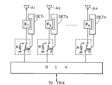
i~, for example, as ~h~wn in Fi~. g.
` In the dr~wing, r~erence nume~ enerally
- d~note~ ~ pha~ed array antsnn~ which ~ nclud~3 a plurallty
o~ antenna ~lements A1~ A~ , ~ . ., and An arrar,ge~ ~t
ln~erval~ of a predet~rmin~d spacln~, phase shlfter~
2, .. ~, and C~ n conn~t~ ~he associated antenna
~lement~, and a divider DIV,.
Mo~e ~pecifically, the ph~sa ~hffler~ 6b 1,
~ 2, ,.~, and ~ n control thei~ pha~ shift amounts on th~
lob~s~ ~ of sl~nal~ rec~ rom ~ controll~r CONT (no~
shown), provide ~ prQdetermlned phas~ shift tg 3~ gnals
recelved from the divid~r ~IV and ~ppl~ th~ phas~-shi~tsd
signals to the a~sociat~d antenna element~ A1, Aa,..~, and
~N; while l:hese phase shift~rs also rec~iY~ signal~
induced in these ~ntenna element~, s1~llarly apply a phas~
shift to ~hs induced ~i~nals and send the pha~e-shi~ted
~ignals to th~ dlvider ~IV which in turn collect~ th~
r~celved pha~e-shift~d signals ~n~ creat~s ~ composite
signal into which the r~csived si~nal~ ar~ combined. Th~
20composite ~ignal is conna~ted, a~ shown in Fig. ~ for
exampl~, through a ~uple~e~ to a tran~ml tter TX and a
receiver RX.
Th~ electric power ~i~tribution rate of the
divide~ DIV and th~ pha~e o~ the ph~s~ shiters ph 1,
nd ~b n ln such ~ phasad array antenna ar~
gen~211y c:ontrolled by p~ovi~ing ~uch ~wi-tchlnc3 ~lements
as PIN diodes or variable react~n~ elements and by
changin~ ~ontrol voltages supplied to ~uch ~lements or by
.~ .,. ~ ., ~
.: . , .
... .
... ~ ,, ', : . .
.. . . . . .
ch~nglng th~ comblnation be~ween the ~lement~ t~ be
swltched.
Meanwhile, su~h a ~emiconduct~r elemen~ as a PIN
dlode i5 r~la~iv~ly mall ln maximum Alilowabl~ hea~
dl~ip~tion and thus th~rs is a dan~er that applicatlon o~
el~ct~ic E)ower exce~ding it~ rated lev~l to the
semlconduct~ element may de~;troy the ~l~ment. For this
~eason, much ca~e must be pald to th~ iconductor
element ln de~iqnlng th~ an~enna.
10~owever, even lf th~ el~ctxi~ power irl th~
respe~tive control ~lem0nts or the h~at dlsslpation
therein aan be ~uppre~ed to b~low th~i~ rated levels, a
troubl~ ~en~r~tlon ln any o~ the many phase ~hirGte~s,
~lvldeF, ant~nna elern~ntx and ~able5 wired therebetween
ill causq mo-~t ~ p~rt ~f electri~ power ~upplied from
th~ divider to ~he ~aulty sy~tem to be refl~ct~ ~rorn ~he
~aulty part and to ~ re-dis~ ut~d to th~ oth~r normal
~ys~em~. ~s ~ r~ult, elect~i~ po~er 6upplied ~o th~
other normal ~ystem~ i~ remark~bly ~nc~e~sed to suah a
2010vel ~s to exceed ~ho aforemontloned allow~ble rated
le~l, whi~h ma~ ~us~ ~h~ do~truction o~ element~ in the
normal ~yst~m~, depen~n~ on the number of ~aulty ~ystem~.
Further, ~ince lnput/ou~put lmpedanco matching
~we~n th~ r~ cklv~ cir~uits ~an b~ maln~ained only
~nder ~uch ~ condl~n that all th~ ~y~tom~ are normal, lf
~v~n on~ o th~ ~ystem~ becom~ ~aulty, th~n thls a~ct2
kh~ other norm~l ~y~tems, thu~ di~a~ling, in som~ cases,
the maint2nance o~ ~h~ im~edanc~ matched conditlon.
1`: ` :
~: "
In thi~ way, th~ prlor art ~ntenna ha~ been
-~ disadvantage~u~ ln that l~ow~r reflectlun or h~a~
dlssipation ~ the lnpu~ Emd output parts of respective
block~ or at th~ int~rn~l ~ircuit~ in th~ normal systems
1~ lncre~sed, thus lncrea~ing the possibili~y of
destructi~n in th~ clrculk ~lement~.
In an att~mpt to r~noYe the above di~ad~ar~g~,
the~e ha~ been ~o ~ provided a m~ans ~or detectin~ th~
presencs or ab~ence ~ a troubl~ in a transmission hlgh-
power ampllr'ler~ Though this attempt aannot dixcriminat~
the trouble loc~tion !out when detecting a tro~le, can
stop th~ ~unction o~ the ~r~nsmitte~
This prior art me~hod, however, 1~ hiqhly
inc~m~enient, bec~use, when a tro~bl~ ~alc~s place even i n
~in~1~ one o~ many antgnna ~ystemsJ thi~ causes the
stoppage o~ ~unctionfi ~f th~ whole systems, thus losirlg
the functiot~s ~. the en~ire cornm~u~icatlon faclliti~s
as~octated with th~ systesn~
For es~arnple, ~lch an ant~a is used in ~ publl~
20 communlcation ~yst~m fo~ ~irplane mounting or ~n another
navigation control comm~rtication ~ystem, which has be~n
r~ntl~ stu~ied, 'ch~ stoppag~ oi~ unctlons in ~he whol~
c~nununicatlon s~ts~m becom~s F~ highly severe problern from
the vieewpoint; ~ a~qty.
Ac~ordingly, ~he pres~n~ lnv~nti~n ha~ n made
~o remove th~ problem$ in th~ ~b~ve pri~ art phasad array
antenna, ~nd it i~ an ~b!ac~ of the inv~n~ion to provid~ a
pha~ rray ~n~nna which, ~ven when one or ones o~
,1
.. , . ~ . .. . ..
~ . . . ..
- . , . - -
, .~ . . .
~:: . . .
.. ~ ~ . ,
~nt~n~ ~y~t~ o~ ulty, ~n ~v~ ~hl~ g~ul~
~r~o~tin~ tho ~un~tlons of kh0 on~ n~
ct~ng th~ oth~ norm~ tonna ~ t~
~ ' '
In ~¢~a~ W~h ~ho ~200n~ ln~on~on, I:ho
~vy~ ~k 1~ b~ p~o~ iASI 11~ ph~ ay
~ntor~r~ in whi~h th~r~ is pr~vid~ r ~ctlng ~h~
p~ c~ n~ Q~ ~ ~r~l~ ubl~ ~n
n~ ry p~t.oX ~n ~ k, ~n~ ~n whiah pOW~F 11~UpF~
r or~ w~r ~uPp~ yE~em~ h~Y~ id
t~o~ oP ~roubl~ urr~d ~ho~n ~ t o~ ~r powor
~u~pl~ o ~ o~ ~y6t~ ~ t~m4 18 con~ a~
n~ ng r~ h~ b~
d ~y ~ ou~ t~c'c~ m~ by
tl~ ~ h~ ~Gub~ ær~co~
o~ho~ no~mal p~ upp~y ~
di~and/~r ~h~se ~h~f~ ln ~ho
1p4~;i~ pOW0~ ~up~l~ qy~m~ o ~ont~ d o~ ~h~
th~ . o~ ~h~ t~inq
m~an~ t~ in~ ~onk~ol ~m~ h~o~
More ~n d~l, on~ or on~ o~ th0 pow~S ~ply
~4n~ ~or a plur~ y o~ ~nt~ m~n~ whieh h~ro a
tro~ble ~r t~ o~ ed tho~:in, ~r~ d~t~t~t
~e~lnsl m~ nd ~aor~n~ to ~h~ tr~ n~litlon~,
th~ ph~ hi~t~r~ ~ th~ ~r ar~ çor~oll~ ~e~ntr~l
moo~) to ~u~o ~h~ optimu~ p~ri~orm~ bta~n~ by t:h*
~h~ no~ wor: ~upply ~ t~
h~ ~n~l m~n~ E~ c~l~d o~
'~
22
providing mernory means or prevlously st~ring th~rein, fo~
ex~mple, combir~ations of tha plurality o~ trou~le power
supply system~ and control algor~ ~hlns optimunl for the
comblnation~ and by sel~ctlnc~ necessary ones of control
~ignal~ on th~ b~si~ o~ the re~ults of th~ d~l:ec'cing mean~
and th~ cor~t~nts of the memory means,
Alternativel~, the control means may be ~rrled
out by providing ~ computer sy~t~m in whi~h th~e cont~ol-
signal set~ln~ algorlthms are stored in tho form of a
prog~am ~nd by ex~cl~ting th~ progr~m to ~n~r~t~ optimum
on~s o~ th~ control slgnals.
As a r~ult ~ with th~ a~ray antenna of ~he
present lnvention, when troubles occur in one3 of the
power supply ~ystems, the trouble pow~r ~-lpply ~ystenn~ ~re
separat~d f ~om th~ r~maining normal sy~;tems, wherel~y th~
in~luence of the ~oubles can be preYen~ea from ~p~ding
ov~r the normal syst~ms and th~ optimum control can be
real~zed wlt:h use o~ th~ remalning normal ~ystems.
Fig~ 1 is a ~lock diaqr~m for explaining a flrst
basic conc~ption o th~ pr~sent lnven~ion;
Figs ~ ~ and 4 ~ho~ exampl~s o~ means f or
det~cl:Lng a trouble in phas~ ~hl~ter~ re~pectively;
FigP 3 i~ a clrcuit di~gram ~howing an example
o~ a ~wi tch;
Fl~. 5 13 a block dl~ram ~or explainlng
~ecot~d b~ conceptl~n o~ th~ prasent inv~ntion
Fig. 6 i~ ~ block diagram ~howln~ an exampl~ o~
, . . . .
. .
.:
: .
. ~ . . . . ..
~lt ~7Z~
a controller in ~ phase~ ~rray an~nna in accord~nc~ wl'ch
the present invention:
Fi~. 7 (a) and (b) ~how block ~iagrams ~howing
- ~xample~ of a pha~e fihi~ter ~ys~,em resp~c~ively7
~lg~ 8 l~ a bloclc diagram for explaining an
exampl~ of phase ~ontrol ln accordance with th~ pr0sent
lnvent;ion; and
Fig. 9 is a ~lock di~gram ~ho~Ying a prior ~rk
phased a~a~ ~ntenna.
1~
The Arrang~m~rlt o~ ~ phase~ arr~y antenn~ and
iks con~rol method in ac~ordance wltl~ th~ pres~nt
ln~enti~n will be detalle~ in th~ foll~wing by r~f~rrln~
to aeconlparlyins drawing3 showlnq th~ir ~mbodlment~. . -
Ref~rln~ fir~t t~ Fi~,. 1, thar~ is ~hown
block dia~r~m ~or expl~lnln~ a ~lrst b,~sic conception o~
the pr~s~nt lnventlon.
In the d~awlng, re~er~nc0 ~yTnbols A1, A2,
and An donot~ ~ plurality ~f antenna~ elements; ~ 1~
5~ 2, ~ . ., ar~d s~ n denote ph~se shi~ters ~ttach~d to ~he
a 3eciat~d ankenn~ el~ment~; and ~V dxnot~a a di~i~er. .
In the pro~ent ~m~odin~nt, furthe~, th~ phase shi~ters
.or ana ~p n are pro-rided at their input and
output ~nd~ wi~h tr~ubl~ det~c~ g circuits DET 1, ~ET
2,..., and ~E'rn re~p3~tiv~ly, an~ switche~ SW 1, SW2,....
and ~Wn a~ w~tll a~ t~rminatin~ r~ tors R are provided
betwe~n th~ pha e ~hit~r~ and the divid~r so that the
respectiv~ swlt~hes SW ar~ open~d and cl~s~d on thQ basis
". ~
: .
~,. . . .. .
32~
o as~o~iated outputs o~ the trouble detectors ~ET.
In thl~ arxan~ement, th~ trouble detQcting
circuits DE1` and th~ tcho~ SW wil l ~e d~tailed l~ter.
If ~ trouble or t~Guble~ occur ln ~ny o~ the phas~
shlft~r~ h~n the as~oci,ated trouble d~tec~or or
detectors DET in the associate~l phase shlt~r system or
slrs~ems g~n~rata a signal or ~ignal~, whlch in ~urn
actuate the ~ssociatod swit~h or swi~ch~s SW, whereby
pow~r to be suppli~d i~rom the di~ider to ~he assoG~ated
phase shi~ter or ~hifter~ i9 ~ent to the a~Qociat~d
termlnat~ ng resistor or resistors P~ to ~nsrgizy the
t~rmin~ting r~lstor or r~istors ~-
As a ~6~5ult:, power to be ~uppli~d to one or ones
o~ the phase -~hifter syst~m~ wh~re ~ trou~le or troubles
ocurred, is cut o~f and the ~s~ociated sy~tem or systems
ar~ termlna~ed at th~l~ sutput ~nds with the prescrlbed
impedanc~ re3i~tanc0 ~o that th~ ph~se shi~'cer system or
sy~tems ~avi.ng a tr~uble or troubles occur~ed th~rein will
not a~ t the other normal phase ~hi~t systems without
cau~lng ~n~ imp~danc~ disturbance~
Ex~l~nation will n~xt be mad~ ~s to a sp0ei~ic
æxampl~ o~ t:he troublo ~tectin~ clrcu~t DET~
Shown in P`ig. 2 i~ an ~ ngement showin~ an
~mbodim~nt o th~ tro~ det~ctor DET, whereln ~trip
line~ S~in ~nd SLout oi~ predet~rmined len~th~ ~re muku~lly
parallelly pro~tid~d a~ spac~d b~r a ~light gap ~em input
and ~utput ~trip li~es IN ana OUT o~ the pha~e hi~ter 9~
so that ~ignal c~rrents lnduc~d in th~ ~tr1 p lln~ in
; .. . .
~ . . . .
: . 1. . .
, . - , , .
32~
and ~Lout ar~ ~eGti~ied by aiod~s D1 and D2, capacltor~ C1
and C2 ana resl~tors R1 andl R2 and then c~p~ed by a
compar~tor COM to detect whlch current ~ ~ larg2r in
magnltud~ ~
Wi~h the abo~e arr~n~ement, occurrenc~ of a
troubl~ in the phas@ ~hlfter ~ c~u~e~ a dl~:Eerence
b~tw~en input ~nd ou~put ~le~tria power to exceed a
predetermin~d ~alu~, wh~r~by the output ~roltage o~ th~
compar~tor ~OM corr~pond~ to the power di~forenc~.
A~cordingly, ~ trouble at l~t in th~ pha~
shifter ~ ~an be d~tect~a by monikoring th~ output
volt~ge o th0 ~omp~r~tor ~
$xplan~tlon wlll n~xt b~ mad~ as to a ~peci~ia
exampl~ o~ th~ ~witch BW~
In ~h~ illu~trat~d embodimer~t, ~uch a circuit a3
~hown in F:lg. ~ li used aq the ~wit~h S~, though the
swltch SW m~ b~ mors ~$mply embodied.,
Th~ cir~ult ~ ., 3 lnclud~s an inpu~ end 11
o~ ~h~ ~3witch SW, a circuit A through which a high
fr~uenc~ current flow~ ln a normal mode, ar~d ~ circuit ~
through whlch a high ~r~qu~ncy current ~lold9 in an
abnormal mod~ ~hen ~ troubl~ ~ak~ pl~ce in th~ a~sociated
ant~nna ~yst~ln.
M~r~ in ~et~ll, the ci~ault A h~ ~ A /4
tran~mlssion line 1~ which l~ conn~c~d ~il;h an ~u~put end
15 o~ th~ switch SW ~hrough ~apacitor~ 13 and 14.
Conn~ctæd betweer th~ capaclt~r~ 13 and 14 ar~ a ~i~de 16,
~ aoil 17 and ~ diod~ 1~ which are conn~ct~d in parallel
. . .. . .. .
, .
~.
.. .
., ., , "
.. .
~ .
; ,, .
:: . , .
2;~
wlth each ot:her ~o th~t ~ bia!; current ba~ed ~n the output
o~ the trouble detector DE'r (not shown ~n Fig. 3) ~lows
~hrouqh th~ coil 17 .
The clrcu:lt la~ on tlle other han~ arranged in
~he same ma~mer as in th~ clr~ult A, ~xcept tha~ the
cir~ult B 1~ connect~d at it~ oukput end with khe
t~rminating r~si~to~ R~
W~th the ~lt~h arr~nged a~ explalned above,
wh~n a bias ~ul~ent ~lows khrough ~he coil 17, a cu~rent
0 1ow~ th~ugh the ~iod~ 16 ~nd 18 and ths diodes are made
~onductive so that the ~ mp~danc~ of the clrcuik A vle~ed
rom ~h~ lnput ~nd 11 become~ 02, which re~ults ln that n~
high ~requeney current will fl~w thr~ugh th~ circuit A a3
v~ew~d from th~ input end 11 and thus the ~ h SW is put
in lts OFF s~a~e.
ilndar ~uch ~ condltion, wh~n no blas c~lrent is
mad~ to flDW t;hrough ths coll 17 in th~ circuit B, on the
oth~r hand, th~ impedan~ of tll~ ~lrcuit ~ viewed fron~ th~
input end 11 becom~ ze~o as cppos@d to the ~lrcui~ A,
whereby a high frequ~ncy cu~ent :~low~ throu~h the ~lrcuit
B and the swltch BW i~ put in its ON ~tata. Therefore,
wh2n th~ both bia~ currents of the ~ir~uits A ~nd B ar~
~ari~d based on th~ ou~put o~ the troubl~ detector ~E~,
th~ switch P,W can ac~ t~a ~n~ the paths o~ the hi~h
frequency ~urrent-~ to th~ circuit~ A ~nd B can b~
~witch~d J
rrh~ tro~l0 det~c~in~ circult DET i3 not
~eskri~t~d to ~he afor~m~nt~oned manner (Fig. 2) and may
n
.
- ;
-
.: ', ~., ,' . ' .. ':
modl~led ln va~lous way~
FOI- ~xampl~, such ~ troubl~ det~ctin~ manner a~
shown in Fig. 4 is considared wherein mean~ ~or d~tecting
a ratio of lnput signal power ~nd ~e~lected pOWer is
provided a~ t:he inpu~ ~nd of the phasa shlf~er ~ ~o th~t
when the power ratlo exceed~ a pred~t~min~d value, ~he
presence o~ a troubl~ iq d~termined.
Further, ~hen such mear2s fo~ measuring the
ref lected power i~ provide~ at th~ lnput end of each
lo sntenn~ ~lemen~, it iB p~s~ibl~ to deteet ~ troubl0 ln the
ant~nna .~le~en~. ~imtlarly, su~h r~Lscted-pow~r
m~a~urlng mearls rn~y be pro~ided at th~ .lnput ~nd o~ the
other block, ~$ a matt:er o~ coursæ.
In accordan~e with a modif lca~ion o~ $h~
embodim2rlt ol~ th~ present invention, th~ corltroller CON~
i~ operated by the ou~put of the troubl* detecting circuit
DEr to con'crol th~ tran~mittar TX, the sw:Ltches ~W, and ~o
on or to display th~ loc tion of the troubl~.
B~ controllinq the array antenna in this mannPr,
20 . th~ influence~ o~ the tro~ on the other normal an~nna
~ystem~ can be r~llably prev~nted.
Th~ a~rangement and control o~ the
a~o~menti~ned array ant~nna are intended, even when a
~rou~le occurs in the ~ntenna ~ystems, 'co avoid the
in~luen~es o~ th~ ~roubl~ on th~ oth~r normal ant~nna
sy~t~ms. Next, d~tail~d expl~natlon will be made a~ to
tha arrangement ~nd ~ont~ol of a pha~ed a~ray antenna
bai~ed on a more dev~loped ex~er~tlon o~ the concept~on o~
..., 11--
.. . .. . . .
., .
: .. ., . : : . .. .. .
. ,
: . . .
.
the foregolng ~rray ant~nna, wherein, even wh~n a trou~le
occurs in antenn~ ~yst~m~, the other norm~l anenna system~
can be controlled to exhibit desired performance~, tha~
is, to satisf~ p~edatermined speci:Eications incll~dlng
~irectivity pattern and beam sweepln~ angl~.
Flg. 5 shows a block di~g~m for ~pl~ining the
second b~ conception o~ thls p~es~n~ lnven~lon.
In th~ drawing, a plu~ality o~ antenn~ ele~ents
Al, A~,.,., and An a3 w~ll a~ ph~se shi~ters C~ 2,
0 and ~b n connec~ed t:o the ~sso~iated antem~ ments are
pro~ided a~ in ~igs. 1 and ~. The pr~sent embodirnent ~f
Flg. 5, however; i~ ferenlt ~rom thos~ o Fl~ 1 and ~,
thRt is, i~ featur~d in that ths divid~r ls repl~ced by
variabl~ dlvider VDIV and troubl~ detectin~ circuits DETl,
DE~2,..., and DETn ~ woll as ~ ~ntrGller cONT are
provlded . t th~ input ~nd output ends of th~ phase
shi~ter-~ ~
The variable divider VDIV, whlch inc~rporates a
welghting clrcuit, ~unctions ~o suitably contr~l electric
power supplled to th~ respectiv~ antenna ~y~tems on ~h~
basis of an output of th~ contrcller CONT.
rrhe controll~r CONT i~ monitoring output ~ignals
from the tr~ubl~ detectors DETl, DET~,..., and DETn~ The
controller CON~, wh~n r~ceivin~ ~ troble detection signal
~rom ~ny Qne o~ khe dete~tors, change~, on the basis ~
~he troubl~ de~ectlon ~ignal/ and ~ends conkrol signals to
the ph~se sh~er~ ., an~ ~b n and/or to the
variable di~,ride~ V~IV to stop pow~r ~uppl~ to the trou~le
; ,. ~ , ` . .............................. . .
.
. . . ~ ,
,., ., ~ ,
~2 ' J ~ %
antenna sys1:em~ and a1so agaln 6et~ th~ lev~1 of power to
be distribu~.ed ~o the ~roubl~ s~stem A~3 well ~s th~ phas~
relationshlps between the phas~ ~hift~rs.
Thls res~t~ing is t:arried ou~, for ~xample, ln
~uch a m~nn~r th~t circulnqtarlces ~uch as th~ nu~ber o~
narm~l arltenna ~ tems ~nd th~ ~o~ltion o~ the sntenn~
array are ~udged, ~nd control i~ e~ected 90 khat the
an~enn~ is put ln il~s best conditi~rls under su~h
circumst~n~e~, that i~, ~o as to 8ati9i~y predet~rmined
performanc~s or ~pecif~ tions ~uch as directivi~y
pattern, beam ~weeping angle and gains in dif~erent
directi~ns .
A~co~ding to this msthod, ~ven when a trouble
t~kes place in any of the plural ant4nna 6~tems, the
other normal ~stems o~h~r than th~ ~roubl~ stem c~n be
operated to se~ura th~ ~unctions of th~ antenna to some
~xt~nt, ~hus enablin~ ~void~ce ~ any ~omm~n~cation
failure of the ant~ u
Then a 8p~Cii~'~ C exampl~ of the controll~r CONT
will be explalned in the ~ollowlng.
Referring to ~iyO 6, ~here i9 ~hown, in ~ block
dl~gr~m form, a part o~ the interior arran~ment o~ th~
controller CONT, which lnclu~e~ a m~lx circuit ~AT ~
discrimln~ln~ ~he pr~ence or ~b~ ce o~ ~ tr~uble
occurrenc~ and th~ troubl~ location on ~h~ basis o~
signals re~eived from th~ tro-lble detecting cir~uit~ ~ET
and for ~on~rerting ~-he di3criminatlQn data int~
pr~deter~ined di5~ital ~l~nal~ to ~a output, ~ memory
~,, . , , ~
~ .. : ~, .. . .
circult ROM havirlg ~on~rol ~lgnals p~Yiou~ly sto~ed
th~3re ln ~or rec~iving the di gital si~nal~ and selecting
c)nes of th~ previously stored control signals which are
as~oc.1ated with ~he digital ~ignals, and ~ control ~l~nal
genera~or CONT~SI(~ for generatlng, ln r~spor~se to the the
signals received ~rom th~ m~mory circuit ROM, second
control signal~ to be ~ent ko th~ pha~ ~hit~rs ~ ~nd/or
the divlder ~IV r~spec~iv~ly.
More ~pecl~i~ally, the memory circuit ROM
lo previc~u~ly storQs the output aontrol ~i~al~ ~ssociated
wlth the troubl~ circwn~t~nces o~ all th~ an~enna ~rstems,
for exampl~ n~ (bl~ train) lndic~ti~ o~ the trou~le
~ir~usnstan~es, in th~ ~orm ~ addr~se~.
The memory ROM pre~riously simulates the nwnber
of trou~l~ sy~tems and the~ combination~, examine~ and
d~termin2s ones o tho control ~l~nals ~tored in th~ RO31
whi~h cau~ the best control of the then no~mal systems
for obtaining th0 be~t functior~,
The control ~ignals of the cont~olle~ CONT
functlon t~ inc~ease or decr~ass the mount o pha e shlft
ln th~ phase shi~r~ in th~ normal 3ys~em~ ~nd/or modi~y
th~ el~e~ric power distribution ratB ~f th~ di~ider.
~he ~tting of phase shi~ and power
distriblltiorl rate in the phase shi~t~rs ~nd ~he divlder i~
differ~n~ dlep~ndln~ ~n tha ph~s~ ifter ~ircuit ~ystem
~nd the divider circuit ~ystem, For eYam~1~2, when th~
phase ~hifter ~stern 1~ o~ a 3dB ~oupler t~ wherein th~
re:Elect~on aoe~fi.cient oi~ a diod~ lq ~Jaried a~ ~hown ln
.. . . ~ , . . ~ ,. .
;-. .; .
~ . . .
. -
2Z
`~ Fig. 7(a), such ~ettlng 1~ carried out ~y changing a
vol~g~ supplied ~o ~h~ di.ode; whlle, when the pha~a
shifter system is of a lln~ swi~ching trp~ wherein ths
leng~h o~ a transmissi~n line 1~ switched ov~r, ~uch
settlng is carried au~ slmilarly by selecting conduct~ve
one ~f diodRs.
~ n ~ddition, for the pu~pose o~ simpllfylng the
storage contents of the memory cira~lt ~OM, the presenco
or absen~e of various ~orts ~P trouble~ ~nd thelr
location~ as well as ~ pro~ram for determining the r~-
~ontrol decidlon pra~edur~ ~ay b~ ~tore~ in th~ memory
ROM.
Mor~ concretely, ~ se~uence aontrol program for
determin~n~ how to ~ontrol the no~mal system~ on the basis
of dat~ read ~ut f~om a trouble syst~m or sy~tems, is
~reviou~ly ~tored in th~ m~mory circult ROM so that the
progr~m is ex~cuted under ~ontrol of a CPU (not shown) to
~enerate c~ntrol ~ignals to b~ output e~ery tlme.
Wl~h ~he memo~y cir~uit ROM arr~nged a3
expla~ned abov~, oven in th~ ~asa wh~re the number o~
antenna sy~t~m~ i~ lar~, the memor~ is adv~n~ageou61y
re~uir~d to have only ~ relatlv~ly ~mall capa~i~y~
In thl~ ~as~, ~h0 troublQ detectlng circuit DET
may h~vs such a c~n~i~uration as show~ in Fig. 3 o~ 4.
Sh~wn ln ~lg. 8 i~ an ~ampl~ o~ tha phas~d
arrAy ~nt~nna wherein 8 ~nt~nna elements aro provided ~o
that, ln th~ eYent whære lt is de~lraa to set the
directivity of ths ~t~nna in a dir~tion corresponding
1~
. -
.; , .
~ ~ -
,~ . ,
to, e.g., 35 degrees with respect to a reEerence
direction, when all the antenna elements and all the phase
shifters are normal, their signals are controlled to have
sequential phase shlfts of about 103.2 degrees for the
phase shl~ter ~ 2, 206.5 degrees for the phase shifter
~ 3,...with respect to a reEerence ~0 degrees of phase
shift) for th~ phase shifter ~ 1, as given in the
uppermost column in the following table.
Under such a normal condition, iE there occurs a
trouble in a sys-tem including the phase shiEter ~ 1 or the
antenna element ~1, then a prior art antenna stops the
function of the entire antenna to avoid the trouble
influence from being extended to the other normal systems
or stops power supply to the -trouble system with the other . .
normal systems being operated as they are, which results
in that it is impossible to obtain desired-directivity
characteristics, as already mentloned above.
TAsLE .L
PHASE I 0 ~l , __ __ __
F.~UL'.'~ , IJ 2 "iJ 3 - P 6 $~ 6 7---- &~ 9 ~ .
NO FAULT ' O 1 0 3.2 2 0 11.5 3 0 9,7 o 5 3 C~ 1 5 6.2 2 5 9.5 2.7
_ , _ _ ~ ..
X O 103.2 206.5 ~ 309.7 63 156.2 259,5
_____ ~ ,_ . . _ ~ .,,
2' X X 0 I 0 3.Z - zn o.s o 1 0 Z,7 1~ 5 Z o 1 5 5,Z C
8 O 103.2 201j.5 3o9~7 o 53 o l 56.2 o 259.5 o X
,. ., " .. _._ _ ,.,, _ .. _ _ ._ .. _ . j
0 7 5~ o ¦ 0 32 2 0 11.5 3 0 9,7 5 3 1 5 6.2 X X
_ . . . . .. _._ ., , ,,
0 3 ' 9'~ o O 1 0 3.:!! X 3 0 9,7 5 3 X 2 5 9.5 2.7
_ __, __ . . _ ~ ~ . . . : `,
,
-16-
~ .7 ~ 22
To avo1d this, in the present invQntion, the
afore~mentloned m~n~ ls u~ed to detect a trou~le locatl~n
and if th~ ph~Re sh~r ~ aulty, th~n khe ph~se
shifer ~ are controlled to have ~uch se~uential
phase ~hl~ts with re~pect to O deg~o~ o~ the r~erenc~
pha~e ~hi~ter ~ 2 as ~ho~n in the ~ecolld co1umn ~rom the
top in Table 1.
Thls ma~hod can improve dir~ctlvi~y
ch~ract~rl~ti~s wh~n ~omp~red ~i~h the case where no
0 modlf~c~tion læ mad~ to phase shi:et control, an~ ~an
provlde ~ theoretical di~tivi~
When ths phas~ ~hi~t~rs ~1 and ~ 2 ~com~ both
faul~y, the similar pha~e ~on~rol 15 ca~ri~d out over the
other normal system~ than th~ ~aulty sy~tems, ~s ~hown by
thQ ~hi~d column f~m th~ ts~p in Table 1.
When troble~ taks place in any ones b~twe~n ths
b~tl3 end pha~ ~hlft~r~ ~1 and ~ 8 sxclu~ive, gor
~xampl~, in the pha~ shl~er~ ~ 3 ~n~ ~ 6, it is
unn~e~sa~y ~o ~odif~ the phas~ of th~ o~h~r phas~
shi~t~r~
R~ference h~ b~en nl~de only to th~ phase shift
qontro1 o~ the ph~s~ ~hlters in ~h~ oregoing
exp1~nat1on, Howev~r, in th~ case o~ a phased arra~
ant~nn~ wh~rein pow~r supplied to th~ resp~ctiv~ ~ntenna
el~ment ~y~t~ms ls weighted, ressttin~ o~ power weight~ to
the normal ~3y~em~ may ~l~o b~ v~lid ~m th~ vi~wp~ink ~
improving p~r~ormancæ~,.
A~ on0 o$ such w~i~ht~ny methoa~, f or examp1o,
17
, ,
~ J ~ , . . .
`'~ ' '
Chebyshe~ weighting ~3 w~93.1 known and may b~ employ~d, but
the pre~ent invent-~ on is not limited to th~ sp~clfic
method .
Further, in order to p~even~ th~ trouble
in1uences ~om ~eing extarld~d to th~ othe~ no~nal
~ystem~, the p~e~nt inventlon may b~ arranged 90 that, E~8
shown in ~lg~ n~ of the pha~e shi$t~rs which occu2red
a troubl~ r~lngl~ t~mlnated at it~ inpu~ or output
~nd with a prescribed re~ifst~r or ~n impedance element to
avoid ilnped~nc~ mism~tching oaused by the troubl0 ~ys~em.
Indu~trial Applicabillt~r:
A9 has ~Qrl expla~ned in the for~going, in
accordarlc~ with a ph~ed array antenn~ o:E th~ ~r~sent
inventiorl, when a t~ or trouble~ tak~ place in any
one or ones oiE a pluralltr o~ power 8u,y?ply s~rs'cems, th~
pha~o control or distl~ibu~ion po~er o~ phas~ shi~ters in
th~ other nvrmal power suppl~ ~ystems is reset r~sponsive
to th~ tro~ situations~ As ~ resul~, the optlmum
control bas~d on the ~rou~ ystem~ can be r~liz~d and
~h~ p~f~mance~ o~ the phas~d array ant~nns c~n b~
improv~d t~ ~ la~go e~stent.
.~.... .. . . .
'' ~ ~ . ' ' '' ' ' :
- . ~
,", .. . .