Note: Descriptions are shown in the official language in which they were submitted.
-
~0o~
CELL BYPASS CIRCUIT
BACKGROUND OF THE INVENTION
Field of the Invention:
The present invention relates to electrical battery
systems. More specifically, the present invention
relates to systems for protecting against failure of
electrical batteries.
While the present invention is described herein with
reference to illustrative embodiments for particular
applications, it should be understood that the invention
is not limited thereto. Those having ordinary skill in
the art and access to the teachings provided herein will
recognize additional modifications, applications, and
embodiments within the scope thereof and additional
fields in which the present invention would be of
significant utility.
Description of the Related Art:
Batteries are used to provide an alternative source
of power for a variety of power supply schemes. As is
known in the art, the failure of a cell in a battery
generally creates an "open circuit" in the system in
which the battery is connected. Unfortunately, in many
applications, such open circuit failure would have
significant adverse consequences. In satellite
applications, for example, the failure of a cell of a
battery would interrupt the power supplied to the
~'
- 2~ i9
processor of the spacecraft. The contents of any
volatile memory may be lost and, accordingly, if and
when power is restored, the system would in effect be out
of place with regard to the tasks being processed. Worse
yet, the system may come up in a condition which would
jeopardize the spacecraft mission, viz., false booster
firing.
The design of satellite processors to circumvent
this possibility is expensive and typically imposes some
performance tradeoffs. Accordingly, the more common
approach has been to provide some means for detecting
and bypassing cell failure. Two techniques are well
known in the art. One involves a network of diodes in
which a diode is coupled in parallel to each cell. In
this configuration, so long as the cell in operative, the
diode is back biased, electrically open and substantially
invisible to the surrounding circuit. When the cell
fails, the diode is forward biased by the current
supplied by the healthy cells and provides a bypass
around the defective cell. While this approach is
effective and inexpensive, the inherent resistance of the
diode drains energy from the other cells and dissipates
it in the form of heat. The power drain forces a
requirement for additional solar panels or battery cells
on the system to protect against this failure mode. The
dissipation of energy in the form of heat may adversely
affect the operation the battery or other sensitive
elements of the system. The often used technique of heat
sinking of the diode adds to the fabrication cost and
weight of the satellite while doing nothing to address
the power drain problem.
An alternative conventional technique involves the
monitoring of the power level of each cell to detect an
impending failure. Voltage levels are telemetered to a
controller or operator at a ground station. The operator
2~69
responds to impending failure data by sending a command
to the satellite to bypass the failing cell in advance of
the open circuit failure. Since the bypass is effected
by a short circuit with virtually no resistance, there is
no power dissipated with this technique. Unfortunately,
effective operation of this system requires the presence
of the human operator to provide the necessary commands
in a sufficiently timely manner. The obvious
disadvantages of predicating successful satellite
operation on the fortuitous presence of a human operator
render this alternative somewhat less than totally
satisfactory.
There is therefore a need in the art for an
inexpensive cell bypass system which automatically
protects against cell failure without draining power from
the system or otherwise adversely affecting system
operation.
SUMMARY OF THE INVENTION
The need in the art is addressed by the cell bypass
circuit of the present invention. The present invention
includes a diode connected electrically in parallel with
a cell of a battery. A thermal switch is mounted in
thermal contact with the diode. A relay including a coil
and a contact is provided. The coil is connected to the
thermal switch so as to be activated by the activation
thereof. The contact of the relay is connected in
parallel with the cell so that the activation of the
diode causes thermal energy to radiate therefrom
activating the thermal switch. The activation of the
thermal switch causes the activation of the relay which
in turn places an electrical short across the defective
20020S~
cell via the contacts thereof.
Various aspects of this invention are as follows:
A cell bypass circuit including:
a diode connected electrically in parallel with said
cell;
a thermal switch mounted in thermal contact with
said diode;
a relay including a coil and a contact, said coil
being connected to said thermal switch so as to be
activated by the activation thereof, and said contact
being connected in parallel with said cell;
whereby the activation of said diode causes thermal
energy to radiate therefrom activating said thermal
switch thereby and the activation of said thermal switch
causes the activation of said relay which in turn places
an electrical short via said contacts across said cell.
A cell bypass circuit including:
a photodiode connected electrically in parallel with
said cell;
a photosensitive means for detecting light emitted
by said photodiode;
a relay including a coil and a contact, said coil
being connected to said photosensitive means so as to be
activated by the activation thereof, and said contact
being connected in parallel with said cell;
whereby the activation of said diode causes optical
energy to radiate therefrom activating said
photosensitive means thereby and the activation of said
photosensitive means causes the activation of said relay
which in turn places an electrical short via said
contacts across said cell.
A method of bypassing a defective cell of a battery
including the steps of:
a) monitoring the current flow through said cell;
b) activating diode means when the current flow
through the cell drops below a predetermined
threshold;
20020~9
~ 4a
c) radiating energy from said diode means on the
activation thereof;
d) sensing the radiation from said diode means;
e) activating a relay based on the radiation
sensed from said diode means; and
f) shorting said defective cell based on the
activation of said relay.
A method of automatically bypassing a defective cell
of a battery including the steps of:
a) monitoring the current flow through said cell;
b) activating diode means when the current flow
through the cell drops below a predetermined
threshold;
c) sensing the radiation from said diode means on
the activation thereof; and
d) electrically bypassing said defective cell
based on the receipt of radiation from said
diode means.
BRIEF DESCRIPTION OF THE DRAWINGS
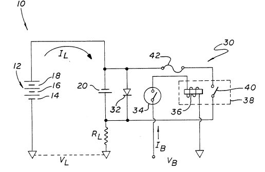
Fig. 1 is a schematic diagram of a preferred
embodiment of the cell bypass circuit of the present
invention.
Fig. 2 is a schematic diagram of an alternative
embodiment of the cell bypass circuit of the present
invention.
DESCRIPTION OF THE INVENTION
The cell bypass circuit of the present invention is
disclosed herein with reference to a preferred embodiment
of Fig. 1 and an alternative embodiment of Fig. 2. Fig.
1 shows the cell bypass circuit of the present invention
- 35 in a typical battery circuit. The battery circuit 10
includes a battery 12 having cells 14, 16, 18 and 20.
For the purpose of illustration, one cell, the fourth
cell 20, is chosen as the defective cell and is therefore
shown separate from the other cells 14, 16 and 18. The
battery operates across some load represented by the
resistor RL. The negative terminal of the first cell 14
~.
~. ~
20020~
~ ~ 4b
is connected to spacecraft structure which is also common
to the other end of the load. An illustrative
implementation of the cell bypass circuit 30 of the
present invention is shown across the fourth cell 20 of
the battery 12.
The cell bypass circuit 30 includes a diode 32
,.
2~2~69
connected in parallel with the cell 20. Note that the
anode of the diode is connected to the anode of the cell
20. Thus, no current flows from cell 20 thru diode 32. A
thermal switch 34 is mounted in close physical proximity
to the diode 32 to facilitate thermal conductivity
therebetween. In the preferred embodiment, the thermal
switch 34 is thermally bonded to the diode 32. The
thermal switch 34 is connected electrically to the coil
36 of a relay 38. A normally open contact 40 of the
relay 38 is connected electrically across the diode 32
via a fuse 42. The fuse 42 is provided in the event the
bypass circuit 30 is false triggered across a healthy
battery cell. That is, in a typical spacecraft
application, the output current of a single healthy cell
may be substantially higher than nominal spacecraft
current. Thus, in the preferred embodiment, the fuse is
chosen to have a rating 4 to 5 times higher than the
nominal spacecraft current rating and 2 to 3 times lower
than the short circuit rating of a single cell.
A bus voltage VB is applied across the thermal
switch 34 and the relay coil 36. In the preferred
embodiment, the cell bypass circuit 30 is built in a
potted cube and bolted onto the battery 12 with pigtail
leads.
In operation, so long as the fourth cell 20 is
healthy, the load current IL from the battery flows into
the load RL and the diode 32 is back biased and off.
When the fourth cell 20 fails, it goes open and impedes
the current flow therethrough. When the drop across the
defective cell 20 exceeds the turn-on voltage of the
diode 32, the diode 32 turns on and begins to conduct.
The load current IL now flows through the diode 32 and
due to the internal resistance of the diode 32, it begins
to radiate thermal energy. The thermal radiation from
the diode 32 is received by the thermal switch 34. When
2~ Q~9
w 6
the thermal radiation of the diode exceeds the threshold
of the thermal switch 34, the thermal switch 34 switches
on and a current IB flows through the coil 36 of the
relay 38. This activates the relay 38 so that the
normally open contact 40 of the relay 38 closes. As the
contact 40 is electrically in parallel with the diode and
the cell 20, the activation of the relay 36 places an
electrical short across the cell 20. Thus, the load
current IL is bypassed around the defective cell 20.
With the defective cell 20 bypassed through the relay,
the diode 32 cools and the thermal switch 34 opens and
removes excitation from the coil 36 of the relay 38.
Relay 38, is of the magnetic latching type and remains
semi permanently in one of either of two possible states
i.e. open or closed depending upon which was the
commanded operation. The open command coil has not been
illustrated in bypass circuit 30 because it is used
during manufacture and ground testing to initialize the
relay 38 to the open state. Other latching relay designs
are possible, including mechanical and electrically
operated latches.
While the present invention has been described
herein with reference to an illustrative embodiment for a
particular application, it is understood that t -
invention is not limited thereto. Those having ordinaryskill in the art will recognize additional modifications,
applications and embodiments within the scope thereof.
For example, a number of sensing and switching schemes
may be employed without departing from the scope of the
invention. This is exemplified in Fig. 2 which shows an
alternative embodiment in which the diode 32 of Fig. l
has been replaced by a light emitting diode 32' and the
thermal switch 34 of Fig. 1 has been replaced by an
optical sensing element 34'. The operation of this
embodiment is essentially the same as that of Fig. l,
2Q~969
-
with the exception that light emitted by the current
sensing photodiode 32' performs the function of the heat
radiation of the diode 32 and optical sensing is used
instead of heat sensing to activate the relay 38. It is
understood that Hall Effect devices may be used for
sensing in place of the diode 32 and that a silicon
controlled rectifier (SCR) or a field effect transistor
(FET) may be used for switching in lieu of the thermal
switch 34.
It is intended by the appended claims to cover any
and all such modifications, applications and embodiments.