Note: Descriptions are shown in the official language in which they were submitted.
~æo~2~87
-- 1 --
1 TITLE OF THE INVENTION
Probe Unit, Driving Method The~!eof, and~
Scanning Device for Detecting Tunnel Current Having
Said Probe Unit
s
BACKGROUND OF THE INYENTION
Field of the Invention
The present invention relates to a probe unit
~or a scanning type of tunnel current detecting device
10 for, for example, a scanning tunnel microscope and a
high-density recording-reproducing apparatus utilizing
the principle of the microscope.
The present invention relates also to a method
for driving a probe suitable for the probe unit.
The present invention further relates to a
~canning-type tunnel current detecting device provided
with the probe unit.
Related Back~round Art
A scannin~ tunnel microscope thereinafter
20 referred to as STM) has already been known which
utilizes the tunnel effect that electric current flows
through a barrier between the surface of a specimen
and a sharp elctroconductive probe brought as close as
several nm or less to the surface. [See ~. Binni~ et
25 al., Helvetica Physica Acta, 55, 726 (1982) USP
4,343,993, etc.]
~g
- - :
, - . ... . . .
~z~
-- 2 --
l The tunnel current which flows on application
..of a voltage between a probe and the surface of a
specimen brought to close proximity of several nm or
less will change exponentially as a function of the
5 distance therebetween. Accordingly, the surface of
the specimen can be observed in high resolution in an
atomic level by scanning the surface of the specimen
in X-Y directions in matrix with the probe with-the
tunnel current kept constant.
A high-density recording-reproducing apparatus
which is based on the principle of the STM is
described in Japanese Patent Application Laid-open
Nos. 63-161552 and 63-161553. In such an apparatus,
recording is conducted, with a probe similar to that .
15 of STM, by changing the voltage applied between the
probe and a recording medium which exhihits memory
effect in its switching characteristics. The material
for the recording medium is exemplified by a thin
layer of a chalco~en compound or of an organic
20 compound having a ~-electron sy9tem. The reproduction
is conducted according to the difference in tunnel
resistance between the recorded portion and the non-
recorded portion of the thin layer. In this type of
recording, recording-reproducing is practicable by use
25 of a recording medium the surface shape of which can
be changed by application of a voltage to the probe.
21~3~2~87
1 Japanese Patent Application Laid-open No. 61-
206148 (1986) describes a probe ~ormed byrutilizing a
processing technique [K.E.Peterson "Silicon as a
Mechanical Material", Proceedings of the IEEE, ~0 (5~,
5 420-457 (1982)] for providing a minute structure on a
substrate, and also describes an STM based on such a
technique. This probe unit is constructed of a
silicon single crystal as a substrate, a parallel
spring made by fine fabrication and being finely
lO movable in X-Y directions, and a tongue-shaped member
having a probe provided on the movable portion so that
the probe may be displaced in direction perpendicular
to the substrate face (in the Z direction) by
electrostatic force caused by an applied electric
15 field between the tongue-shaped part and the bottom
face portion.
Japanese Patent Application Laid-open No. 62-
281138 describes a memory device provided with a
converter array in which tongue-shaped parts as
20 disclosed in Japanese Patent Application Laid-open No.
61-20S148 are arranged in a multiple manner.
In conventional probe units of a cantilever
structure, there are posed, for example, the following
disadvantages (1) to (4).
~1) The probe, since it is provided on the
tip end of the cantilever, tend~ to positionally
~ . . ,: , ; . ,
2~2~87
I ~eviate slightly by thermal expansion or constriction
of the cantilever in the length direction, or by
deformation caused by difference in thermal expansion
coefficient between the can~ilever material and the
S electrode material.
(2) A cantilever constituting a probe is
difficult to be formed precisely because of liability
of causing warpage or torsion by the internal stress
in preparation thereof. The cantilever is also liable
10 to be deformed by internal stress relaxation with a
lapse of time. Accordingly, a cantilever is
unsatisfactory for a probe-driving mechanism which is
required to have position-controllability with
precision of an atomic level. A multiple arrangement
15 of cantilevers, for example, as shown in the above-
mentioned Japanese Patent Application Laid-open No. 62-
281138, is required to maintain the mutual positional
relation in high precision. The cantilever, however,
could not satisfy such requirement.
(3) In the aforementioned prior art, the
substrate is prepared by finely processing a silicon
single crystal, and the material for the substrate is
limited to silicon, which needs many steps of ,
production processes, resulting in a disadvantageous
25 high cost.
(4~ Further in the prior art, the driving
.
"' ' '~ " ' .' ! . ' ~
2l~ 187
- 5
1 mechanism has a plurality of probes on parallel
hinges. Therefore, on driving cach of the probes in a
z direction, each probe may be deviated by
electrostatic force, causing mutual interference of
5 the probes, if the parallel hinges are not
sufficiently rigid.
SUMMARY OF THE INVENTION
An object of the present invention is to
10 provide a probe unit which overcomes ~he above-
mentioned disadvantages of the prior art, and which is
affected little by a temperature change in the
operation, and allows a precise positional control at
an atomic level when the probes are arranged in a
15 mUltiple manner.
Another object of the present invention is to
provid~ a probe unit which can be prepared with a high
precision without occurrence of warpage and torsion in
the production.
A further object of the present invention is
to provide a method for driving the probe.
A still further object of the present
invention is to provide a scanning type of tunnel
current detecting device which is designed compactly,
25 operable by a low voltage, affected little by external
vibration, and capable of stable scanning.
. ~ : .
.:
.. .
.
2~ 87
1 These object~ are achieved hy the preSQnt
invention described below
~r ~
According to an aspect of the presen~
invention, there is provided a probe unit comprising a
5 substrate, a bridge-shaped flexible member formed on
the substrate, and a probe provided in contact with
the flexible member, the probe unit further comprising
a driving means for displacing the probe in a
direction perpendicular to a face of the substrate.
According to another aspect of the present
invention, there is provided a probe unit comprising a
substrate, a first electrode formed on the substra~e,
a bridge-shaped flexible member formed on the
sub~trate and insulated by a cavity from the first
15 electrode, and a probe provided in contact with the
flexible member, the flexible member being constituted
of a laminate comprising a second electrode layer, an
insulating layer, and a third electrode layer for
applying a voltage to the probe. .
According to still another aspect of the
present invention, there is provided a probe unit
comprising a substrate, a first electrode formed on
the substrate, a piezoelectric layer formed on the
first electrode, a bri.dge-shaped flexible part formed
25 on the substrate, and a probe provided in contact with
~he flexible member, the flexible member being
-
-" 2~2~7
1 constituted of a laminate comprising a second
electrode.~ayer, an insulating layer, and a third
electrode layer for applying a voltage to the probe,
and the first electrode and the second electrode layer
5 being in opposition to each other with interposition
of the piezoelectric layer.
According to a further object of the present
invention, there is provided a probe unit comprising a
substrate, a bridge-shaped of flexible member formed
10 on ~he substrate, and a probe provided in contact with
the flexible member, the flexible member being
constituted of a laminate comprising a beam structure
layer, a first electrode, a piezoelectric layer, a
second electrode layer, an insulating layer, and a
15 third electrode layer for applying a voltage to the
probe.
According to a still further aspect of the
present invention, there is provided a method for
driving a probe unit comprising a substrate, a first
20 electrode formed on the substrate, a bridge-shaped
flexible member formed on the substrate and insulated
by a cavity from the first electrode, and a probe
provided in contact with the flexible member, the
flexible part being constituted of a laminate
25 comprising a second electrode layer, an insulating
layer, and a third electrode layer for applying a
37
I voltage to the probe; the method comprising displacing
the probe in a direction perpendicular t~ the ,
substrate face by an electrostatic force caused by
application of voltage between the first electrode and
5 the second electrode layer.
According to a still further aspect of the
prese~t invention, there is provided a method for
driving a probe unit comprising a substrate, a first
electrode formed on the substrate, a piezoelectric
10 layer formed on the first electrode, a bridge-shaped
flexible member formed on the substrate, and a probe
provided in contact with the flexible member, the
flexible member being constituted of a laminate
comprising a second electrode layer, an insulating
lS layer, and a third electrode layer for applying a
voltage to the probe, and the first electrode and the
second eleGtrode being in opposition to each other
with interposition of the piezoelectric layer; the
method comprising displacing the probe in a direction
20 perpendicular to the substrate face by piezoelectric
effect caused by application of voltage between the
first electrode and the second electrode layer.
According to a s~ill further aspect of the
present invention, there is provlded a method for
25 driving a probe unit comprising a substrate, a bridge- !
shaped flexible member formed on the substrate, and a
.
. , :
-
. .
187
1 probe provided in contact with the flexible member,
sal`d flexible member being constituted of a laminate .
comprising a beam structure layer, a first electrode
layer, a piezoelectric layer, a second electrode
5 layer, an insulating layer, and a third electrodelayer for applying a voltage to the probe; the method
comprising displacing the probe in a direction
perpendicular to the substrate face by piezoelectric
effect caused by application of voltage between the
10 first electrode layer and the second electrode layer.
According to a still further aspect of the
present invention, there is provided a scanning type
of tunnel current detecting device having a probe unit
comprising a substrate, a bridge-shaped flexible
15 member provided on the substrate, a probe provided on
the flexible member, and a driving means for
displacing the probe relative to the substrate; an.
ad~usting means for adjusting the distance between the
probe and a specimen to be observed; and a voltage
20 applying means for applying an voltage between the
probe and the specimen.
BRIEF DESCRIPTION OF T~E DRAWINGS
Fig. l illustrates a cross-section of the
25 first embodiment of the probe unit of the present
invention.
.
87
-- 10 --
1 Fig. 2 illustrates a plan view of the first
embodiment of the probe unit of the present invention.
Fig. 3A through Fig. 3D illus~rate the steps
of forming the probe unit of Fig. l and Fig. 2.
Fig. 4 illustrate the cross-section of the
second embodiment of the probe unit of the present
invention.
Fi~. 5 illustrates a plan view of the second
embodiment of the probe unit of the present invention.
Fig. 6A through Fig. 6E illustrate the steps
of forming the probe unit of Fig. 4 and Fig. 5.
Fig. 7A and Fig. 7B illustrate respectively
the cross-sectional view and the plan view of the
third embodiment of the probe unit of the present
15 invention.
Fig. 8 shows a schemAtic view of arrangement
of a plurality of the probe units.
Fig. 9A through Fig. 9C illustrate principal
steps of ~orming the probe unit of Fig. 7.
Fig. lO, Fig. ll, and Fig. 12 illustrate
constitution of the probe units employed to tunnel
current detecting devices.
DETAILED DESCRIPTION OF THE PREFERRED EMBODIMENTS
The bridge-shaped flexible member in the
25 present invention has a structure of a both-end fixed
beam ~n wh1ch the both ends of the flexible member are
:, .
, ,
187
fixed on a substrate.
The flexible member is specifically . .
constituted of a laminate comprising at least an
electrode layer, an insulating layer, another
5 electrode layer for applying a voltage to the probe,
the laminate being connected to the substrate by at
least two supports. The shape of the flexible member
i5 not limited.
Scanning of ~he probe can be made under less
10 influence from external vibra~ion by raising the
natural vibration frequency of the flexible member
: because the probe is formed on the flexible member
provided on the substrate.
The probe unit having the structure of the
15 present invention will not cause warpage nor torsion
of the flexible member in the production of the probe
unit because the probe unit is produced by laminating
an electrode layer, an insulating layer, and another
electrode layer for application of voltage to the
20 probe and then processing and etching by
photolithography technique~
The driving means suitable for the probe unit
of the present invention include those employing
electrostatic force, and those employing piezoelectric
25 effect, among which those employing a piezoelectric
effect are more preferable for a larger stroke of the
,~ ., ..:
~.- ~ . -,
Z~ L87
- 12 -
1 probe.
~ The probe units and the methods of driving the
units are described in detail by referring to the
following Emb,odiments 1 to 4.
5 Embodiment 1
An embodiment of the present invention is
explained by referring to the figures. Fig. 1 and
Fig. 2 are a cross-sectional view and a plan view for
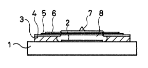
e~plaining a probe unit of the present invention. On
10 a substrate 1, a lower electrode 2 is provided. A
support 3 is etched on and around the lower electrode
2 to form a cavity 8, thus an upper electrode 4, an
insulating film 5, and a probe electrode 6 are formed
in the shape of a bridge. Further on the probe
15 electrode, a probe 7 is provided which serves to
detect electric current ~enerated by a tunnel effect.
The probe i~ placed so as to keep equal the distances
from the support 3 of the bridge. The force driving
the probe ~ in a direction perpendicular to the
20 substrate face is an electrostatic force, which causes
displacement of the probe by application of a voltage
to the lower electrode 2 and the upper electrode 4.
The probe displacement mechanism is constituted of a
both-end-supported beam, allowing displacement
25 strictly perpendicular to the substrate face.
~he insulating film 5 serves to insula~e the
2~ 187
- 13 -
l probe 7 detecting tunnel current generated, and the
probe Plectrode 6 (electrically connected to the probe
7) from the upper electrode 4.
For example, in the case where the bridge has
5 a length of 200 ~m, a breadth of 20 ~m, and a
thickness of approximately 1 ~m, and the distance
between the electrodes is 3 ~m, ~he application of 50
V between the lower and the upper electrodes causPs a
displacement of approximately 1 ~m in the direction
10 perpenducular to the substrate face (in an Z axis
direction). Additionally, this structure gives a
resonance frequency of as high as 200 KHz of the
flexible member, enabling scanning with less influence
of external vibration.
The probe unit of this structure is driven
specifically as described below.
Several ten volts of an offset voltage is
initially applied between the electrodes. The
reduction of the voltage restores the probe on the
20 bridge-shaped, both-end supported beam to pull out the
probe in a Z direction owing to its elasticity, while
the increase of the voltage strengthen fur~her the
a~racting force to pull in the probe in the Z axis
direction, whereby the driving is feasible in the Z
25 direction~
The steps of forming the probe unit of Fig. 1
' ~
2~ 2~8~
- 14 -
1 and Fig. 2 is described by referring to Fig. 3.
Step _
A glass plate made of glass 7059 supplied by
Corning Co. having a thickness of 1.1 mm was employed
5 as the substrate 1. Thereon chromium was deposited in
a thickness of 0.1 ~m by vacuum vapor deposition, and
processed by photolithography to form the low~r
electrode 2;
Step B
Subsequently, copper as the supporter 3,
titanium as the upper electrode 4, a silicon oxide
film as the insulating film 10, titanium as the probe
electrode 11, and tungsten as the probe material 9
were deposited thereon by a successive sputtering
15 method in thicknesses of 3.0 ~m of copper, 0.2 ~m of
titanium, 0.6 ~m of silicon oxide, 0.2 ~m of titanium,
and 3.0 ~m of tungsten.
Step C
The successively formed five-layered film
20 prepared in the Step B was processed consecutively by
etching with a hydrofluoric acid type etching solution
to give a pattern of the upper electrode 4 in Fig. 2.
Then according to photolithography, the portion except
above the lower electrode 2 was covered with a
25 photoresi~t, and copper of the support 3 was over-
etched with a hydrochloric acid type e~ching solution
- 15 -
I to form the ca~ity 8.
In this Embodiment, the etching pattern or the
over-etching state should be controlled in such a
manner that the support which is made of copper is
S insulated from the lower electrode 2. In the case
where the support is of insulative material, such
control is not needed.
Thereafter the probe electrode 11 was
processed to give a pattern 6 in Fig. 2 by
10 photolithography. Then the insulating film 10 was
fabricated to give a pattern denoted by the numeral 5
in Fig. 2 by photolithography. Further the probe
material 9 was over-etched with a sodium hydroxide-red
prussiate type etching solution to form a probe 7 of
15 tungsten. Thus the probe unit was prepared.
Since the probe unit described above is formed
by employiny a photolithography technique and a vacuum
film-formation technique, the substrate employed may
be of a low-priced material, and the unit can be mass-
20 produced. The means for applying a voltage betweenthe upper electrode and the lower electrode provides a
mechanism for displacement in the Z direction for each
probe, thus enabling individual adjustment of the
surface unevenness and the surface height deviation
25 arising in the probe formation. This probe unit is
advantageous also in that the probe is capable of
'
Z0~ 37
- 16 -
I moving in the completely perpendicular direction, and
exhibits extremely high resonance frequency.
Embodiment 2
A second embodiment is described below.
5 Fig. 4 and Fig. 5 are a cro~s-sectional view and a
plan view respectively for explaining a probe unit of
the present invention. On a substrate 1, a support 43
is provid~d. The support 43-has a cavity 49. A low r
electrode 42 and a piezoelectric layer 44 are provided
l0 in the cavity and brou~ht into contact with the
substrate 1. Further, on the support 43 and the
piezoelectric layer 44, an upper electrode 45, an
insul~ting film 46, and a probe electrode 47 are
formed in the shape of a bridge. On the probe
lS electrode, a probe ~ is provided which serves to
detect electric current generated by tunnel effect.
The probe is placed so as to keep the distances equal
from the support of the bridge. The probe 7 is driven
in a ~irection perpendicular to the substrate face by
20 ~pplying a voltage between the upper electrode 45 and
the lower electrode 42 to deform the piezoelectric
layer 44. The change of the polarity of the upper
electrode and the lower electrode enables an up and
down displacement of the probe in the Z direction.
25 Additionally, the probe displacement mechanism is
constituted of a both-end-supported beam, allowing
,, :~ : , . .. .
, , , , , .:
21U C~2~7
- 17 -
l displacement strictly perpendi~ular to the substrate
face. -
The insulating film 46 is provided to serve toinsulate, from the upper electrode 45, the probe 7 and
5 t~e probe electrode 47 electrically connected with the
probe 7.
For example, in the cass where the bridge has
a length of 200 ~m, a breadth of 20 ~m, and a
thickness of approximately 1 ,um, and the piezoelectric
10 layer has a height of 3 ~m, the application of 30 V
between the lower and the upper electrodes causes a
displacement of approximately 1 ~m in the Z direction.
The steps of forming the probe unit of Fig. 4
and Fig. 5 is described by referring to Fig. 6A
15 through Fig. 6E. Fig. 6A through Fig. 6E illustrate
produstion steps by a cross-sectional view at the line
a-a in Fig. 5
step A
A glass plate made from glass 7059 supplied by
20 Corning Cc. having a thickness of 1.1 mm was employed
as the substrate 1. Thereon chromium was deposited in
a thickness of 0.1 ~m by vacuum vapor deposition, and
processed by photolitho~raphy to form the lower
electrode 42.
25 Step B
Subsequently, as the support 43, 44, a
21~1~2~87
- 18 -
l piezoelectric material, aluminum nitride (AlN) was
formed in a film thickness of 3 ~m by RF mag.netron ..
sputtering by using AlN as the target under the
conditions of a back pressure of 10 7 torr, an argon
5 pressure of 5 x 10 3 torr (N2 : 50 %~, the RF power of
5 W/cm2 and the substrate temperature of 350 C.
Thereafter, on the support 43, 44, titanium as
the upper electrode 45, a silicon oxide film as the
insulating film 46, titanium as the probe electrode
lO 47, and tungsten as the probe material 48 wer~
deposited by a successive sputtering method in
thicknesses of 0.2 ~m of titanium, 0.6 ~m of silicon
oxide, 0.2 ~m of titanium, and 3.0 ~m of tungsten.
Steps C and D
The successively formed five-layered film
prepared in the Step B was processed consecutively by
etching with a hydrofluoric acid type etching solution
to give a pattern of the upper electrode 45 in Fig. 5.
Then according to photolithography, the probe
20 electrode 47 and the insulating film 46 were processed
into a pattern of Fig. 5. The probe material 48 was
also processed into a pattern of the probe electrode
47 as shown in Fig. 5. Thereafter in order to provide
~he cavity 49, a photoresist layer 61 was formed
25 except above the portions corresponding to the cavity
49 which are at the both sides of the piezoelectric
, :
37
-- 19 --
l layer 44 to be kept remaining. (Fig. 6C is a cross-
sectional view at the line c-c in Fig. 6D)
Step E
Subsequently, the support and piezoelectric
5 material 43, 44 was over-etched with an aqueous acetic
acid-nitric acid solution to form the cavity 49 by
photolithography. In this Example, the etching of the
pattern or the state of the over-etching should be
controlled in such a manner that the support 43, 44
10 which is a piezoelectric material of AlN is insulated
from the lower electrode 42 and that the cavity in a
desired shape is obtained. Finally, the probe
material 48 was over-etched with a sodium hydroxide-
red prussiate type etching solution to form a tungsten
15 probe 7. Thus the probe unit was obtained.
Embodiment 3
A third Embodiment of the present invention is
descr~bed below by referring to Fig. 7A and Fig. 7B.
In Fig. 7A and Fig. 7B, the numeral l denotes a
20 substrate; 3, a support; 8, Q cavity; and the portion
on the support constitutes a bridge--shaped both-end
supported beam 70. The both-end-supported beam 70 is
constituted, from the bottom, of a beam structure
layer ~l, a lower eiectrode layer 72, a piezoelectric
25 materlal layer 73, an upper electrode layer 74, an
insulating layer 5, an electrode layer 6 for applying
2~2~L8~
- 20 -
1 a voltage to the probe, and an electroccnductive probe
7 through which the tunnel effect current flows. The
probe 7 is placed at the central position of the bo~h-
end-supported beam ~0O
The driving of ~robe ~ in the direction
perpendicular to the substrate surface (the Z
direction) is conducted by utilizing expansion-
constriction of the piezoelectric material 73. That
is, the application of a voltage to the piezoelectric
10 material 73 having been treated for polarization from
the lower electrode 72 and the upper electrode 74
expands the both-end-supported beam lengthwise to
cause deflection of the both-end-supported beam by the
difference of the expansion from that of the beam
15 structure layer, thus driving the probe 7.
The steps of forming the probe unit
illustrated in Fig. 7A and Fig. ~B is described by
referring to Figs. 9A, 3B, and 9C.
Step A
A glass plate of 1 mm thick was employed as
the substrate 1. Thereon copper as the support 3, a
rsilicon oxide film as the beam structure layer 71, and
titanium as the lower electrode 72 were deposited by a
successive sputtering method in thicknesses
25 respectively of 3.0 ~m of copper, 3 ~m of a silicon
o~ide film, and 0.2 ~m of titanium. Thereon 3 ym of
.
,
:." ' ~- ~ '' :.:,
- 21 -
l aluminum nitride was deposited as the piezoelectric
material 73 by RF magnetron spu~tering. Further
thereon titanium as the upper electrode 74, a silicon
oxide film as the insulating film 5, titanium as the
5 electrode 6 for applying a voltage to the probe,
tungsten as the probe material 75 were deposited by
succsessive sputtering in thicknesses respectively of
0.2 ~m of titanium, 0.6 ~m of the silicon oxide film,
0.2 ~m of titanium, and 3.0 ~m of tung~ten.
lO Step B
The four layers from the probe material 75 to
the upper electrode 74 out of the successively formed
film of the Step A described above was processed by
pho~olithography into a pattern shape of the beam
15 structure layer 71 in Fig. 7A by etching the four
layers successively with a hydrofluoric acid type
etching solution. Subsequently, the piezoelectric
material (aluminium nitride) 73 was similarly
processed with glacial acetic acid-nitric acid etching
20 solution.
Further the three layers of from the lower
electrode 72 to the support 3 were successively
proce~sed with a hydrofluoric acid type etching
solution. Then, according to photolithography, the
25 portion except above the cavity 8 in Fig. 9A was
covered with a photoresist, and over-etched the copper
.
- 22 -
1 of the support 3 with a hydrochloric acid type etching
solution to form the cavity 8.
Step C
Subsequently, according to photolithography,
5 the seven layers of from th~ electrode layer 6 for
probe voltage application to the support 3 were
processed sequentially to give the patterns shown in
Fig. 7A. Then the probe material 75 was over-etched
with a sodium hydroxide-red prussiate type etching
10 solution to form the tungsten probe ~.
Embodiment 4
A tunnel current detecting apparatus is
explained in which a probe unit of Embodiments 1 to 3
is incorporated.
Fig. 10 shows a cross-section of the
apparatus. The numeral 101 denotes a probe unit
provided with a plurality of the probes of the present
invention. The probe unit is fixed to a Z-axis coarse-
adjusting piezoelectric element 103 for coarse
20 adjustment in the Z direction to bring the probe unit
101 close to the opposing surface of the specimen 102
so that a tunnel current is detectable. The
inclination of the fixing member 104 which fixes the Z-
axis coarse-adjusting pi~zoelectric element 103 is
25 adjustable by three inclination-adjusting screws 106,
thereby the degree of parallelization between the
2Ci~3Z~87
- 23 -
1 probe unit 101 and ~he surface of the spe~imen 102
being correctable. The numeral 105 denotes a parallel
hinge spring stage which has double parallel springs
combined in rectangular cross as shown in the plan
5 view of Fig. 11, thereby the specimen 102 placed on
the center being moved freely in X-Y directions. The
drive of the specimen is made by piezoelectric
elements 107 and 108. 5uch a constitution allows the
probe to scan the surface of the specimen ~02 in X-Y
10 directions, thereby keeping constant the distance
between the surface and the probe by adjusting each
probe independently in correspondence with the fine
roughness and inclination of the surface by employing
the Z-axis driving mechanism for each probe.
In this Embodiment, the specimen is moved in
the X-Y directions and the probe is movable only in
the Z direction, so that the movement in the X-Y
directions does not interfere with the movement in the
Z direction, thus stable scanning being practicable.
Another constitution is shown in a cross-
sectional view in Fig. 12, in which a cylindrical
piezoelectric element 109 is employed, in place of the
~forementioned parallel hinge spring stage 103, as the
s~age for fine movement of the specimen 102 in the X-Y
25 direction. The probe unit 101 is fixed to a fixing
member 110, and opposing to the face of the specimen
~2187
- 24 -
l 102 fixed to the cylindrical piezoelectric element
109 .
On the peripheral surface of the cylindrical
piezoelectric element 109, the electrode is divided
S into four parts opposing to the X-Y directions.
Application of a reversed polarity voltage to the
opposing electrodes makes the cylinder minutely
incline to the direction of the opposing electrode,
moving the specimen 102 finely in the % or Y
10 direction. Application of the same polarity voltage
on the quartered electrodes expands or constricts the
cylinder in the Z direction, allowing the coarse and
fine adjustment in the Z direction, so that the
specimen 101 is brought close to the probe unit 101.
15 Although the adjusting screw for correction of
inclination is not shown in the figure, they may be
attached in accordance with the necessity.
The present invention has the advantages a~
below.
(1) The probe unit of the present invention
seldom causes a positional deviation o~ the probe
arising from lengthwise thermal expansion caused by
temperature change in operation or from the difference
of thermal expansion coefficient between the flexible
25 member and the electrode material, because of the
symmetrical structure having the probe in the middle
I
. . . , . -: , .
" . ~ ,:;. - .. :.,.~ . .
., , :. . . . -
-: . , ~ . , :
~ . . ..
2~ 7
1 of the bridge-shaped flexible member provided on the
substrate and the fixation of the both end of the
flexible member.
The probe unit can be formed precisely without
5 warpage nor torsion of the beam caused by inner stress
in production.
(2) The probe unit of the present invention
can be produced in extremely low cost because the
material of the substrate is not limited to
10 conventional silicon substrate but may be usual 7059
glass or the like.
(3) The utilization of piezoelectric effect
particularly increases the driving force in the Z
direction, and maintain the displacement in the Z
15 direction in the level same as in a cantilever even
with ~he bridge-shaped structure.
It also raises the resonance frequency,
enabling the probe to respond to a higher scanning
without influence of external vibration.
~ : :, . , ,, : - - - :,- : ,