Note: Descriptions are shown in the official language in which they were submitted.
21D~22~3
HIGH PERFORMANCE INTEGRATED CIRCUIT CHIP PACKAGE
AND METHOD OF MAKIN~ SAME
Field of the Invention
This invention relates to thermal and
electrical packaging of integrated circuit chips and more
particularly to a thermal and electrical chip package
which provides high density electrical interconnection
and packaging for high speed, and high power dissipation
for chip cooling, and methods of fabricating such high
performance integrated circuit chip packages.
Backqround of the Invention
A major hurdle in the production of high
performance computers is the electrical and thermal
packaging for very large scale integration (VLSI) and
ultra large scale integration (ULSI) chips. While high
performance VLSI and ULSI chips have been designed to
include up to several million devices thereon, a major
problem still exists in connecting these chips together
and dissipating the heat produced. A high performance
integrated circuit chip package must provide for high
density electrical interconnection and thermal stability
2 0 of integrated circuit chips.
It will be recognized that the electrical and
thermal performance of integrated circuit packaging may
represent conflicting design parameters. For example, an
increase in package size may decrease the heat
25 dissipation capability required per unit area. However
such an increase in package size will increase the path
~OC)~ 3
--2--
length between chips and thereby increase the propagation
delay. On the other hand, placing the chips closer
together maximizes speed while requiring a large number
of chip connections in a small area and high heat
dissipation per unit area.
One well known high performance chip package is
the Thermal Conduction Module (TCM), which is described
in u.s. Patent 3,993,123 to ~ugh et al., and in an
article entitled "Thermal Conduction Module: A High
Performance Multilayer Ceramic Package," by A.J. Blodgett
and D.R. Barbour published in the IBM Journal of Research
and Development, Vol. 26, No. 1, P30 (January 1982). The
TCM includes a multilayer ceramic substrate which is
capable of providing connections for about 100 integrated
circuit chips, each dissipating up to a maximum of 3-4
watts. The substrate, formed of fired alumina ceramic,
includes up to 33 internal wiring layers therein, and
about 1800 brazed input/output pins on the bottom surface
thereof for connecting to the next level of packaging.
Integrated circuits are mounted on the top surface of the
substrate, using the well known controlled collapse chip
connection ("C-4"), or solder bump technology. A
cylindrical piston is spring biased against the back of
each chip to provide a heat conductive path to a water
cooled housing consisting of a cover or hat and a cold
plate, the cold plate having suitable chambers for
circulation of water. A metal C-ring is compressed
between the hat and substrate frame to form a hermetic
seal, and helium gas is provided in the hermetically
sealed area for further heat conduction.
While the TCM represents a significant advance
in multi-chip packaging, there are a number of
limitations therein which make it unsuitable for high
power high density VLSI and ULSI chips. For example,
power dissipation is limited to about 3-4 watts per chip
notwithstanding the elaborate cooling scheme. The
multilayer ceramic substrate also possesses a number of
2(~1~Z;~:13
shortcomings. First, the alumina substrate has a
coefficient of thermal expansion which is quite different
from that of the silicon integrated circuit chips,
resulting in sufficient thermal mismatch such that the
size of the chip is severely limited. use of larger
chips would result in stress-related reliability
problems. The C-4 joints between the integrated circuits
and the substrate provide a buffer between the thermal
mismatch; however, the inflexibility of these joints
provides a limit as to the size of integrated circuit
chips which may be employed. Moreover, in order to
properly align the 30 or more layers of the multilayer
ceramic substrate, the conductive lines and vias internal
to the substrate must be thick. A large number of layers
must therefore be formed to provide all of the conductors
necessary for chip connections. The large number of
layers and the vias connecting them result in significant
unwanted inductances and capacitances. The large number
of layers also create potential yield problems. Since
the entire substrate must be formed before it may be
tested, a defect in any internal layer requires the
entire substrate to be scrapped. Finally, the piston and
spring arrangement for heat removal creates large
mechanical stresses on the chips and requires a
hermetically sealed helium environment for added heat
dissipation. This scheme also severely limits the heat
removal capability of the package.
The art has provided many improvements on the
basic TCM in an attempt overcome these shortcomings. For
example, U.S. Patent 4,092,697 to Spaight describes a TCM
in which a thermal liquid material enclosed in a film is
mounted between the chips and heat sink. U.S. Patent
4,639,829 to Ostergrin et al. discloses a truncated solid
conical piston which includes a thin layer of high
thermal conductivity grease between the piston and heat
sink for added heat dissipation. U.S. Patent 4,617,730
to Geldermans et al. discloses a method of forming a chip
2~;2 2~3
interposer which is placed between a multilayer ceramic
substrate and an integrated circuit chip to provide thin
film redistribution interconnections. Finally, an
article entitled "High Performance Heat Sinking for VLSI"
published by D.B. Tuckerman and R.F.W. Pease in the IEEE
Electron Device Letters, Volume EDL-2, No. 5, May, 1981,
at page 126, discloses a use of a large number of small
fluid channels for cooling an integrated circuit chip.
Notwithstanding these and other improvements, the TCM
does not provide a dense enough or powerful enough
package for VLSI and for future generations of ULSI
chips.
Summary of the Invention
It is therefore an object of the invention to
provide an integrated circuit chip package which provides
high density interconnection and high power dissipation
for integrated circuit chips.
It is another object of the invention to
provide an integrated circuit chip package the component
parts of which are easy to fabricate using known
techniques.
It is another object of the invention to
provide an integrated circuit chip package in which
thermal mismatches between the chips and the package are
25 ; ni ; zed.
It is another object of the invention to
provide a chip package which conducts heat without the
need for piston and spring arrangements.
It is yet another object of the invention to
provide a chip package which may be tested during
intermediate fabrication steps, and reworked if
necessary.
These and other objects are provided by an
integrated circuit chip package which employs three
unique and interrelated elements for high performance
thermal and electrical characteristics. The first
element is a support substrate having conductors or
2~ L3
5--
connectors extending from one face to the opposite face
thereof, and a multilayer wiring substrate on the
opposite face of the support substrate for connecting the
front face of integrated circuit chips mounted thereon to
one another and to the conductors by C-4 like or other
suitable attachment techniques. The second element is a
heat sink having microchannels formed therein at one face
thereof, while the third element is a thermally
conductive cushion material connecting the one face of
the heat sink with the exposed backside faces of the
integrated circuit chips.
In particular, the support substrate is a
monolithic block of fired ceramic, having a coefficient
of thermal expansion which matches that of silicon, and
having metal filled vias extending therethrough from one
face to the opposite face thereof. In a preferred
embodiment the support substrate is aluminum nitride or
silicon carbide with molybdenum filled vias.
Input/output connectors, for example bra~ed pins or pads
are provided on the one face of the support substrate for
connection to the next level of packaging. A multilayer
wiring substrate on the opposite face of the support
substrate includes a number of thin film insulating
layers having conductive vias and a conductive plane
therein. The thin film layers are formed on the support
substrate one at a time using a self-aligned thin film
process described below. Such thin films are formed by
semiconductor-type chip fabrication processes. The
integrated circuit chips are mounted on the exposed
surface of the multilayer wiring substrate using C-4
solder bump or other mounting means.
It will be noted by those having skill in the
art that since the support substrate may be, in its
simplest implementation a single layer substrate, it may
be fabricated of a material whose thermal coefficient of
expansion more closely matches that of the silicon chips,
rather than alumina as used in the TCM. Accordingly,
213
minimal stress is placed on the C-4 solder bumps or
balls, so that larger size integrated circuit chips may
~e used. Moreover, since all of the power, ground and
signal planes are provided in a thin film multilayer
wiring substrate, a dense interconnection pattern with
reduced resistive, capacitive and inductive parasitics
may be formed, compared with the TCM's thick film
multilayer ceramic substrate. Since dense
interconnection patterns may be formed, all power, ground
and signal interconnections may be formed using about six
layers, in contrast with thirty or more layers required
in a multilayer ceramic substrate. Also, since the
multilayer wiring substrate is built up on the support
substrate one layer at a time, each layer may be tested
after it is formed, and if defective, may be reworked
prior to forming the next layer.
According to another aspect of the invention,
the heat sink includes microchannels formed therein at
one face thereof. This heat sink is also formed of
material having a coefficient of thermal expansion which
closely matches that of silicon; for example fired
silicon carbide. Microchannels may be machined in the
fired silicon carbide. Alternatively, the silicon
carbide heat sink may be formed around organic
microchannel rods which vaporize during the firing
process leaving the silicon carbide heat sink with the
microchannels formed therein. In another implementation,
the microchannels may be molded using powdered silicon
carbide or silicon carbide firing mixture. The
microchannels are placed as close to the one face of the
heat sink as possible, consistent with mechanical
rigidity and stability. The microchannels provide a high
degree of heat transfer compared with a single large
channel or plenum interior to the heat sink. The
structural and thermal considerations which influence the
precise structural configuration of the channels within
the heat sink structure have been described in "A Thermal
2~2~L3
--7--
Module Design for Advanced Packaging" by L. Hwang, I.
rrurlik and A. Reisman, J. Electronic Mat., ~ol. 16, No.
347 (1987).
According to a further aspect of the invention,
a soft, thermally conductive mechanical cushion ~aterial
is used to connect the microchannel end of the heat sink
to the exposed back faces of the chips. The thermally
conductive mechanical cushion material is sufficiently
thin to efficiently conduct heat from the integrated
circuits to the microchannel area through the wall of the
heat sink while being sufficiently thick and soft to
provide a mechanical cushion against the dimensional and
positional variations between the integrated circuits and
the heat sink surface. In a preferred embodiment the
heat sink is a low melting point metal, such as pure
indium. The indium is placed between the chips and heat
sink, and is reflowed to form a conformal layer
therebetween. The indium mechanical cushion eliminates
the TCM's complex system of pistons or fluid enclosed
bags. Moreover, the indium, which can be thought of as
solder in this application, together with the
microchannel heat sink provides sufficient thermal
conduction so that hermetic sealing and a helium
atmosphere around the chips is not required (although it
may be provided).
In the method of making the chip package
according to the invention, the support substrate and the
multilayer wiring substrate thereon are formed. The
chips are mounted on the exposed face of the multilayer
wiring substrate using well known C-4 solder bump or
other suitable mounting technology. The heat sink and
microchannels are formed and the microchannel face of the
heat sink is placed adjacent to the exposed faces (back
side surfaces) of the chips with a preform of the thermal
cushion material therebetween. The entire assembly is
then heated above the preform melting temperature, but
below the melting point(s) of the C-4 solder connections,
2~ 3
or any other component of the package, while maintaining
a predetermined distance between the heat sink and the
substrate with a support ring. The preforms melt and
conform to the exposed faces of the integrated circuit
chips and the face of the heat sink adjacent the
microchannels.
According to another aspect of the invention, a
method is described for forming a self-aligned thin film
multilayer wiring substrate on a support substrate. Each
layer of the multilayer wiring substrate includes
conductive vias (for connecting one layer to another) and
conductive planes (for power, ground, redistribution and
signals) insulated from one another as appropriate. For
each layer, the conductive vias are formed by forming
holes in an insulating layer to uncover selected ones of
underlying vias and/or conductive planes. Then,
electroless plating is used to build up the conductive
vias on the underlying vias or conductive planes.
Conductive planes are formed in an insulator by etching
the required pattern extending beyond selected ones of
the underlying vias, using a photoresist and known
lithographic techniques. A thin conductive film is
evaporated on the patterned photoresist and insulator,
and a well ~nown "lift-off" technique is used to dissolve
the photoresist and conductive film thereon, leaving the
conductive film only on those areas which were previously
etched in the required pattern. Electroless plating may
be used to build up the conductor plane on the conductive
film. The conductive vias may be solid conductors, for
example copper or may be clad on the top, bottom and
sides with a layer of chromium, nickel or an alloy
thereof, for better adhesion or other purposes such as
providing enhanced resistance to corrosion.
Since the method of forming the multilayer
wiring substrate uses high density thin film techniques,
all wiring may be accommodated in about six layers
(compared with more than 30 layers for multilayer ceramic
~2213
_9_
substrates). Moreover, electroless plating of conductors
from underlying conductors provide self alignment of
vias, enabling aggressive ground rules for via
positioning, while lift-off and electroless plating
provides self-aligned planes. Clad conductors provides
better adhesion. Finally, since each layer is formed
separately, the partly formed substrate may be tested,
and rewor~ed if necessary, before forming the next layer.
It will be recognized by those having skill in
the art that the support substrate and multilayer wiring
substrate of the invention may be employed in conjunction
with other less efficient cooling techniques for
integrated circuit packages; for example in conjunction
with the spring loaded piston of the TCM. It will also
be recognized by those having skill in the art that the
microchannel heat sink and thermally conductive cushions
of the invention may be employed in conjunction with
other chip support subs~rates; for example multilayer
ceramic substrates. However, it will also be recognized
by those having skill in the art that the combination of
the support substrate including the multilayer wiring
substrate, the microchannel heat sink and the thermally
conductive cushion material forms a unique integrated
circuit package which
provides for highly dense packaging with highly efficient
heat transfer.
Brief Description of the Drawings
Figure 1 is a schematic cross sectional view of
the high performance integrated circuit chip package of
the present invention.
Figures 2A and 2B are graphs describing the
variation in temperature and shear strain for various
thickness of indium cushion.
Figures 4A-4E illustrate a method of forming
self-aligned vias in a multilayer wiring substrate
according to the present invention.
Figures 5A-5E illustrate a method of forming
2~2;213
--10--
self-aligned conductor planes in a multilayer wiring
substrate according to the present invention.
Figures 6A-6D illustrate a method of forming
clad metal vias or signal, power or ground planes in a
multilayer wiring substrate according to the present
invention.
Description of the Preferred Embodiment
The present invention now will be described
more fully hereinafter with reference to the accompanying
lo drawings in which a preferred embodiment of the invention
is shown. This invention may, however, be embodied in
many different forms and should not be construed as
limited to the embodiments set forth herein; rather
Applicants provide this embodiment so that this
disclosure will be thorough and complete, and will fully
convey the scope of the invention for those skilled in
the art.
Like characters refer to like elements
throughout. For greater clarity, the thickness and
relative thicknesses of the layers have been exaggerated,
and the figures have not been drawn to scale.
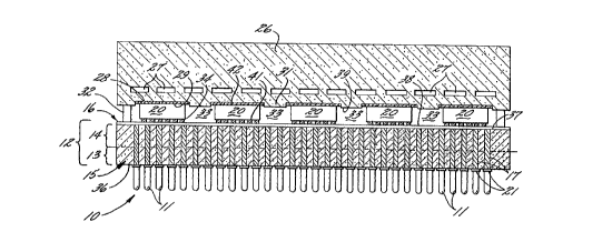
Referring now to Figure 1, there is shown an
overall schematic cross sectional representation of the
high performance integrated circuit chip package of the
present invention. As shown in Figure 1, integrated
circuit chip package 10 comprises three major components:
substrate 12 which itself comprises support substrate 15
and multilayer wiring substrate 16; heat sink 26 which
includes a plurality of microchannels 27 therein; and
cushions 28 formed of a thermally conductive low melting
point, easily deformable cushioning material for
transferring heat from chips 20 to heat sink 26. Each of
these elements will now be described in detail.
Substrate 12 comprises support substrate 15 and
multilayer wiring substrate 16. Support substrate 15
primarily provides support for multilayer wiring
substrate 16, although it may also provide a significant
'
2~L3
--11--
degree of added heat dissipation capability because of
its thermal conductivity. Support substrate 15 includes
conductors 17 which extend from one face 36 to the
opposite face 37 thereof. Support substrate 15 is formed
of a material which has a coefficient of thermal
expansion similar to that of silicon. In one embodiment,
silicon carbide (SiC) is chosen because its coefficient
of expansion (3.7 X 10⁻⁶/~C) closely matches that of
silicon (3.0-3.24 X 10-C). In addition, silicon carbide
is a very good thermal conductor, having a thermal
conductivity of 70-270 w/mk~ compared with the alumina
substrate used in the TCM which has a thermal
conductivity of 20 w/mk~. Furthermore, silicon carbide
is a mechanically strong material, having a Young's
modulus of 410GPa, compared with lgOGPa for silicon. In
special applications, silicon itself or beryllium oxide
may be used for support substrate 15. Since support
substrate includes closely spaced conductors 17 therein,
the dielectric constant of the substrate may be enhanced
(at the expense of some thermal mismatch with silicon) by
using aluminum nitride for support substrate 15.
Aluminum nitride (AlN) has a coefficient of thermal
expansion of 3.3-4.4Xl0-6/~C, a thermal conductivity of
230 w/mk~ and a Young's modulus of 300-310 GPa. It has a
25 dielectric constant of 9.3 compared with 20-30 for
silicon carbide. Alternatively, other ceramic materials
may be used.
Support substrate 15 may be formed as follows:
a monolithic block of silicon carbide, silicon nitride,
silicon or other material having a thermal coefficient of
expansion which matches silicon is fired to provide a
unified structure a~cordin~ to well known techniques.
Then, holes are drilled from side 36 to side 37, using
laser drilling or conventional mechanical drilling.
Alternatively, a material may be formed in the shape of
conductors 17, and a block of silicon carbide or silicon
nitride may be pressed and formed around the material.
L3
Then, the structure is fired. During firing the
conductor-shaped material may decompose and/or evaporate
leaving channels, which are then filled with a conductor.
Alternatively, the structure may be slip-formed from
powder by techniques well known in the ceramic
manufacturing art. Molybdenum is preferred for conductor
17 because its thermal coefficient most closely matches
silicon carbide. Alternatively, tungsten or other metals
or alloys may be used. The holes or channels may be
filled with conductor by first coating the walls of the
channels with Mo-Ni alloy using an electroless deposition
process. The channels may then be filled with Cu-Ag
alloy which is brazed into the channels. If necessary,
the filled substrate may be fired again to solidify
conductors 17.
A number of input/output connector pins 11 are
attached to support substrate 15. The pins may be brazed
to pads 21. Alternatively, pads 21 alone may be the
input/output connector for surface mount technology. In
a preferred embodiment, a pin grid array of 2590 pins may
be formed with 2.5mm between pin centers, on a 9cm X 9cm
substrate area. For an llcm X llcm substrate, 3872 pins
may be accommodated. As is well known to those having
skill in the art, a high input/output count is a critical
requirement for advanced packaging of VLSI/ULSI chips.
Referring again to Figure 1, multilayer wiring
substrate 16 is formed using a self-aligned planarized
thin film process, the details of which are described
below in connection with Figures 4, 5 and 6. The
structure of multilayer wiring substrate 16 will be
described below in conneckion with Figure 3. Integrated
circuit chips 20 are mounted on exposed surface 38 of
multilayer wiring substrate 16 using controlled collapse
chip connection (C-4) solder balls 34. As is well known
to those having skill in the art, C-4 technology permits
the total surface of the chip as opposed to only its
edges to be used for input/output connections. Because
2~ 3
-13-
there is an excellent thermal match between the chips and
the substrate of the present invention, and there is a
small chip temperature rise due to the excellent heat
dissipation capabilities of the package, a large size
chip (for example 2cm on an edge or more), may be used.
This compares with the 0.4-0.5cm on an edge chips
currently used in TCMs due to the thermal mismatch
between the silicon chips and the alumina multilayer
ceramic substrate. Moreover, the presence of a large
number of C-4 joints also alleviates a heat dissipation
problem to some extent, since heat is also removed
through these joints, as described by A. Reisman et al
"Heat Dissipation From Silicon Chips in a Vertical Plate
Elevated Pressure Cold Wall System", J. Electronic Mat.,
Vol. 11, No. 391 (1982). It is indicated, for example,
that heat conduction is enhanced by as much as 17% due to
the presence of 12lC-4 contacts between the chip and an
interconnection support substrate.
Heat sink 26 is preferably formed of a material
having a thermal coefficient of expansion similar to
that of silicon and close to that of the support
substrate. As discussed in connection with support
substrate 15, silicon carbide may be used, although
silicon or other ceramic materials may also be used.
Since the dielectric constant of heat sink 26 is
irrelevant, SiC or AlN might be used. Microchannels 27
may be formed in heat sink 26 using laser or mechanical
drilling or using an organic fill. Laser drilling will
provide smoother microchannels which are more amenable to
laminar fluid flow therethrough, while mechanical
drilling or organic fill will provide rougher
microchannels to thereby enhance turbulent flow.
Microchannels 27 are formed as close to face 39 of heat
sink 26 as is possible consistent with the mechanical
rigidity necessary to prevent deformation or warpage of
the microchannels. In a preferred embodiment, using
turbulent fluid flow, channels which are about lmm deep,
2~1~)22~3
-14-
spaced lmm apart and having a width of about 5mm are
formed lmm below the surface. Such a configuration was
deduced from the results of extensive analyses described
in the publication by L. Hwang et al previously
referenced. The heat sink 26 and substrate 12 may be
10.16cm X 10.16cm (6" X 6") and may carry up to 25 chips.
The effective cooling area of the heat sink is 9cm X 9cm.
In one specific implementation, each chip is a lcm square
and is spaced 0.8cm apart from the other chips. In such
a module it has been found that 1000 watts (40
watts/chip) may be dissipated with a maximum temperature
rise on a chip of only 12~C with respect to the
temperature of the input water. For the worst power
case, where all chips except the one at the inlet end are
powered to 40 watts per chip, the maximum variation of
temperature between chips is also less than 12~C. These
results will allow use of 25 VLSI/ULSI chips in the
package. It is recognized that since such power
dissipation demands are rare, the actual chip temperature
rise will be much less. ~his worst case number, 12~C, is
to be compared with conventional cooling designs which
allow for 60~C or greater temperature rises above ambient
temperature conditions. Such temperature excursions may
affect chip reliability and always result in performance
degradation since circuit designs must take worst case
temperature excursions into account.
Cushions 28 will now be described. Cushions 28
provide a thermally conductive path between the exposed
back faces 42 of chips 20 and heat sink 26; and provide a
cushion which accommodates aspirates, tolerances and
thermal expansions between chips 20 and heat sink 26. In
particular, it is well known that when C-4 solder balls
34 are employed, chips 20 will have a considerable
variation in parallelism and in depth. It is also known
that thermal expansion may cause the distance between
chips 20 and heat sink 26 vary. Accordingly, cushion 28
must be sufficiently thick to be able to absorb movement
13
between chips 20 and heat sink 29 during thermal cycling,
yet sufficiently thin to act as a good thermal conductor
between chips 20 and heat sink 26.
~he preferred material for cushion 28 is a low
melting point ductile material of high heat conductivity.
This material may be thought of as a solder. One
preferred solder is pure indium (melting point 156.6~C).
Indium is a preferred solder because it has the highest
thermal conductivity (o.8~C/W/cm2) of the low melting
point elemental materials which can serve as solders
(including Pb, Sn, Bi, Ga, Cd and As~, and undergoes
creep deformation (is very ductile) at very low stresses.
Also, pure indium is preferred because small additives of
other materials (i.e. alloys of indium) can be used to
decrease the creep rate for a given applied stress
relative to pure (99.999~) indium thereby reducing
compliance.
Referring now to Figure 2, the worst case chip
to chip temperature variation (Figure 2A) and worst case
indium shear strain (Figure 2B) for various thickness of
indium will be described in order to illustrate how the
thickness of indium cushion 28 may be chosen. For
purposes of obtaining the specific data depicted in
Figure 2, a package design having a 5 X 5 array of lcm X
lcm chips 20 on a 1.8cm pitch were employed. It was
assumed that chips 20 were reflow bonded to substrate 12
with 95Pb5Sn C-4 connectors 34, each such connector
having a 125um nominal diameter and a nominal height of
75um on a 250um pitch. Each chip 20 has a 37 X 37 C-4
connector array for a total ofi 1357 connectlons (3
connectors removed from each corner). Substrate 15 was
assumed to be a 4in. X 4in. AlN substrate with post fired
molybdenum conductors 17. Multilayer wiring substrate 16
was assumed to consist of a copper ground plane and 2-6
signal and reference planes in a polymeric dielectric.
Electroless nickel vias may be employed. Heat sink 26
was assumed to be densified reaction-sintered silicon
~22~3
-16-
carbide with 10% silicon. There were assumed to be 15,
lmm X 5mm water channels 27, with a total flow rate of
550 cc/s through heat sink 26.
To account for wide variability in the possible
power dissipation exhibited by the 25 chips in the
package, four cases were considered in Figure 2; i.e.
power dissipation of 10 and 40 w/cm2 in chips 20 and 0 and
5 w/cm2 in multilayer wiring substrate 16. Referring now
to Figure 2A, the worst case chip to chip temperature
variation is shown for various thicknesses of indium
cushion. It will be seen that due to the high thermal
conductivity of indium, increasing indium thickness only
has a small influence on worst case chip to chip
variation. Referring now to Figure 2B, indium shear
strain is shown for various thicknesses of indium
cushion. It will be seen that because of indium's high
ductility it requires about 500~m thickness before shear
strain becomes small and therefore insensitive to further
cushion thickness. Thus, if minimal distortion is
desired, a 500~m minimum thickness cushion will provide
near minimum shear strain consistent with small chip to
chip temperature variations. Since the chip to chip
height variations due to C-4 height variations across
package 10 may introduce up to a +145~m variation in
cushion thickness, a nominal thickness of 650~m cushion
should be provided. For other package designs graphs
similar to Figure 2A and 2B may be designed, empirically
or by simulation techniques, and the optimum thickness of
cushion 28 may be chosen. As was described above,
cushion 28 is chosen to be sufficiently thick to cushion
the variation of thermal mismatches between chips 20 and
sink 26 while providing effective thermal coupling
between chips 20 and heat sink 26.
Referring again to Figure 1, a support ring 32
is used to determine the nominal cushion thickness, upon
indium reflow. A support ring thickness of 1250~m is
specified to produce desired indium thickness of 500~m.
2~2Z~3
-17-
The support ring should be of a rigid material to protect
the assembly package from any mechanical stresses during
handling. A hermetic seal may be provided between
substrate 12 and heat sink 26 for protecting integrated
circuits 20 and solder ball connections 34 and for
providing additional cooling using helium or other high
conductivity ambient atmosphere if necessary. It will
also be seen that support substrate 15 may be formed of
pin support substrate 13 and wiring support substrate 14.
Substrates 13 and 14 may be formed as was described with
respect to support substrate 15. Two substrates (13 and
14) may be employed so that brazing of pins 11 may be
performed on one substrate (13) and thin film multiwire
substrate 16 may be formed on another substrate (14) in
separate operations. Then, both substrates may be
combined using brazing or other well ~nown techniques.
Referring now to Figure 3, multilayer wiring
substrate 16 will be described. Substrate 16 is formed
on support substrate 15, and includes a first insulating
layer 51 and a conductive power plane 52 formed thereon.
A conductive via for connecting power plane 52 with one
conductor 17 in support substrate 15 is not shown.
Second insulating layer 53 includes a plurality of metal
filled vias 54 therein. Optional silicon dioxide
insulating layer 56 may be formed on insulating layer 53.
Ground plane 57 is formed on first insulating layer 53
(or on optional layer 56). A second via layer 58 and a
third insulating layer 59 are also included. Similarly,
a Y signal plane 61 an X signal plane 62 and top surface
metallurgy 63 is included with via layers 58, 66 and 67
and dielectric layers 59, 68 and 69 and optional silicon
dioxide layers 70, 71 and 72, respectively, therebetween.
Top surface metallurgy 63 connects multilayer wiring
substrate 16 to solder balls 34.
As may be seen from Figure 3, all of the
interconnection wiring among chips 20 and between chips
20 and pins 11 may be provided using only four layers of
2~
-18-
thin film wiring, i.e. ground plane 57, power plane 52, Y
signal plane 61, and X signal plane 62. This is as a
result of using thin film self-aligned processes to form
multilayer wiring substrate 16, and contrasts sharply
with the TCM's thick film multilayer ceramic substrate
process in which 30 or more layers are required for
power, ground, redistribution, X and Y signal planes.
For the embodiment described herein, the distance 74
between a wiring plane and a via is about 6um while the
thickness 76 of a via layer or wiring plane is about 4um,
and the width 77 of a via is about 14um.
Referring now to Figure 4, a self-aligned
method of forming a layer of filled vias (for example
vias 54, 58, 66 or 67 in Figure 3) according to the
invention, will be shown. It will be recognized by
~hose having skill in the art that this process may be
repeated to form the requisite number of via layers.
Referring now to Figure 4A, insulating layer
51, comprising polyimide, for example DuPont PI2525
polyimide, Hitachi PIQ13 polyimide or Dow Chemical's
Bis - (benzocyclobutene) based material (Product code
HXU13005.02L), 4-lO~m thick, is deposited on an
underlying layer (for example support substrate 15) using
conventional spin deposition and is fully cured by
heating through a range of temperatures to 400~C. It
should be noted that all the insulating layers in
multilayer wiring substrate 16 may be formed as above.
Then, power plane 52 is deposited by evaporating,
sputtering, CVD or any other suitable method, a layer of
copper, or layers of chromium, copper and chromium for a
total thickness of 4~m. Referring now to Figure 4B,
insulating layer 53 is spun on and cured at 250~C.
Referring to Figure 4C, a l~m layer 56 of optional
silicon dioxide or other suitable material such as
silicon nitride is deposited on insulating layer 53 by
Plasma Enhanced Chemical Vapor Deposition (PECVD) at
300~C, and layer 81 of photoresist 4~m thick is deposited
2~2;~3
thereon. Photoresist 81 is then patterned. The
patterned photoresist 81 and underlying optional
insulating layer 56 are etched with layer 53 acting as an
etch stop. PECVD SiO2 may be etched in SF6 at a rate of
10~m/min.
Referring now to Figure 4D, a reactive ion etch
is performed on insulating layer 53 using an etch of
10sccm ~2 and 50sccm N2 at 2KW, which yields a selectivity
relative to the photoresist greater than 10 to 1, i.e.
the insulating layer 53 etches 10 times faster than its
overlying photoresist layer. While conventional reactive
ion etching techniques may be employed a preferred
reactive ion etching may employ a split magnetron system
at 1-2~m/min. Such a split magnetron system is more
fully described in U.S. Patent 4,738,761 to Bobbio et al.
Optional layer 56 may be left on or removed.
Referring now to Figure 4E, a self-aligned
conducting via 54 is formed by first etching the top most
chromium layer in power plane 52 (if present) using an
etch of 1:1 H2O/HCL etch solution. Then, the surface to
be plated is activated using a PdCl2 solution, and an
electroless plating of 8~m nickel is performed.
Electroless plating prevents copper from forming on
insulating areas 53 and will only allow nickel to form on
the exposed palladium sensitized portion underlying power
plane 52.
Referring now to Figure 5, the method of
forming conductor wiring planes (for example power plane
52, ground plane 57, Y signal plane 61 or X signal plane
62) will be shown. One preferred technique uses a lift-
off process. The process will be illustrated for X
signal plane 62 which lies on via 66. Referring to
Figure 5A, a 4~m insulating layer 69 is spun and cured at
250~C.
Referring to Figure 5B, a 4~m layer 83 of
photoresist is spun, cured and patterned using well known
techniques. Then, (Figure 5C) a reactive ion etch is
2~1~2;~13
-20-
performed into insulating layer 69 as was described with
respect to Figure 4D. As illustrated in Figure 5C, the
etch uncovers an area extending beyond via 66. SIO2 layer
71 acts as an etch stop. Then, (Figure 5D) a O.Ol~m
layer of palladium 86 is evaporated. As will be seen in
Figure 5D, layer 86 deposits on planer regions 86a, b and
c, but not on sides 87 because of the retrograde profile
of the composite insulator-photoresist structure. Then
the photoresist is dissolved, lifting off the evaporated
palladium (86b and c) in the process, according to a well
known lift-off process. After the lift-off patterning
has been effected, only layer 86a remains. Then (Figure
5E) electroless plating of nickel 8~ takes place using
palladium ~6a as an activator. Accordingly, self
alignment of the dielectric area is obtained by using the
palladium activated lift off process.
It will be understood by those having skill in
the art that the process described above provides for
self alignment of vias and conductor patterns. It will
also be understood by those having skill in the art that
high density is provided by using thin film processes.
It will also be understood that after each self-aligned
layer is formed, it may be tested prior to forming the
next layer. If a layer is defective it may be etched
away or the entire partially formed multilayer wiring
substrate may be removed down to support substrate 15 and
the process may be restarted. This contrasts with the
known multilayer ceramic substrate in which 30 or more
layers must be formed and then fired before the substrate
may be tested. While Figures 4 and 5 describe a
preferred self-aligned thin film process, it will be
recognized by those having skill in the art that other
processes, including those for forming multilevel chip
metallization layers, may be employed.
Referring now to Figure 6, an alternate method
of forming a via, for example via 54 of Figure 4E, will
be described. It has been found that the better
2~ 13
-21-
conducting film thin metals suffer from poor adhesion to
commonly used dielectric materials, for example
polyimide. Gold, for example, adheres poorly to
polyimide, while copper tends to oxidize during polyamic
acid conversion to polyimide, resulting in the failure of
adhesion at the copper oxide-polyimide interface. In
order to overcome the problems of poor adhesion, it is
known to clad the upper and lower surface of a thin ~ilm
conductor with a metal from the class of metals which
form metalocenes, for example nickel and chromium.
However, the cladding of a nickel or chromium layer above
and below a copper or gold thin film conductor does not
prevent separation of the conductor from the sidewall,
which is known to occur. According to the present
invention, a method of cladding the sidewall of a thin
film conductor is provided, to form a completely clad
conductor; i.e. a conductor clad on the top, bottom and
side.
Referring now to Figure 6A, there is shown a
portion of power plane 52, near first via 54, the
fabrication of which was described in Figure 4e. As was
shown in Figure 4E, first via 54 lies on power plane 52
which in turn lies on first insulating layer 51. As
shown in Figure 6A, first via 54 may lnclude intermediate
copper layer 91, bottom cladding layer 92, typically
chromium, nickel or alloys thereof, and top cladding
layer g3 typically chromium, nickel or alloys thereof.
Second insulating layer 53, shown in Figure 4E, has been
removed.
Referring now to Figure 6B, cladding layer 94
comprising chromium, nickel or an alloy thereof or other
suitable metal or alloy is sputtered onto power plane 52.
The sputtering, because of the pressure at which it is
conducted, results in conformal coating. Then (Figure
6C), an anisotropic etch, for example ion mill or
reactive ion etching, is employed to remove the
horizontal portions of cladding layer 94 leaving only
.
- : .
.. . .
2C~13
-22-
sidewall cladding portion 96 thereon. Insulating layer
97 is then coated onto the structure as shown in Figure
6D. As may be seen in Figure 6D, conductor 91 now
includes upper cladding layer 93, lower cladding layer 92
and side cladding layer 96 thereby resulting in a
completely clad conductor with superior adhesion
characteristics.
It will be understood by those having skill in
the art that other metals may be used for cladding layers
92, 93 and 96 and that an electroplating rather than a
sputtering technique may be used to deposit cladding
layer 94 in Figure 6B. The etchant gases for the
reactive ion etching step depend on the metallurgy
employed. For example, for chromium, CF4 is employed
while for NiCr, Cl2 is employed.
Referring once again to Figure 1, the method
for forming package 10 according to the invention will
now be described. In forming this package, it is
critical that stress absorbing cushions 28 have the
lowest melting point or deformation temperature of all
components used. According to the method, substrate 15
and multilayer wiring substrate 16 are formed as was
described above. Pins 11 may be brazed to substrate 15
before or after multilayer wiring substrate 16 is formed.
Alternatively, as described above, pins may be brazed to
pin support substrate 13 and multilayer wiring substrate
16 may be formed on wiring support substrate 14 and then
substrates 13 and 14 may be joined. Chips 20 are then
mounted on multilayer wiring substrate 16 using C-4
solder connections (bumps) 34. It should be noted that
the melting point of C-4 solder connections (bumps) 34
must be higher than the melting point of cushions 28 so
that the solder balls do not remelt when the cushions are
formed.
Heat sink 26 having microchannels 27 therein is
formed and substrate 12 having integrated circuits
thereon and heat sink 26 are brought together. A solder
22~3
-23-
preform may be used for cushions 28, with the preforms
held in place using grooves 31 cavities 28 or a
combination thereof. Alternatively, a single preform may
be used across the entire width of heat sink 26. Once
brought together, the entire assembly is heated above the
melting temperature of cushion 28, with the distance
between substrate 12 and heat sink 26 being maintained by
the support ring 32 at a predetermined thickness.
Cushions 28 melt and reflow to form a conformal cushion
between heat sink 26 and integrated circuits 20,
accommodating separation irregularities between the chips
and their underlying substrate in the process. The
assembly is then allowed to cool.
In the drawings and specification, there have
been disclosed typical preferred embodiments of the
invention and, although specific terms are employed, they
are used in a generic and descriptive sense only and not
for purposes of limitation, the scope of the invention
being set forth in the following claims.