Note: Descriptions are shown in the official language in which they were submitted.
1
IMPROVEMENTS IN OR RELATING TO OVERVOLTAGE PROTECTION
CIRCUITS
The present invention relates to an overvoltage
protection circuit and is especially but not exclusively
suited to use in a telephone line.
A telephone line from a telephone exchange to the
subscriber's apparatus carries the voice signal and also a
power supply to the subscriber's apparatus. Usually, the
power supply consists of a d.c, voltage of about 40 volts.
Hitherto, the voice signal has been an analogue signal
representing the waveform of the voice. In future develop-
ments of telephone systems the analogue voice signal is to
be replaced by a digital signal and in accordance with the
ISDN (integrated services digital network) system the bit
rate of the digital voice signal is 144 k bits/s and higher
bit rates. Imbalance of the conductors of a telephone line
is not troublesome for the analogue voice signal since the
frequencies involved are less than 5 kHz and although some
of the control signals transmitted down the line use
frequencies up to 20 kHz no significant interference or
other difficulties have been encountered. On the other
hand, when high bit rate digital data is transmitted along a
telephone line it is very important that the line is
balanced so that radiation of the data signals and the
picking up of interfering signals is avoided. To this end,
there are specific requirements laid down in certain
countries defining the permissible degree of imbalance
between-the conductors of a telephone line. In Germany,
for instance, the requirement is that the balance should be
better than -66 dB (1 in 2000).
Overvoltage protectors are commonly provided in
telephone lines to limit the voltage on the Line relative to
ground and the differential voltage between the conductors
of the line, the requirement for such protectors being made
more important by the increasing use of semiconductor
circuitry in telephone apparatus in place of the hybrid
2 ~~J~2~~~.~
transformers and other similarly robust but bulky
components.
Figure 1 shows an example of a conventional
overvoltage protection circuit connected to a telephone
line.
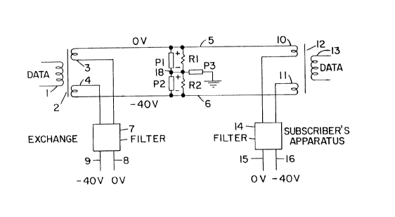
In Figure 1, data to be carried by the telephone line
from an exchange is applied to a winding 1 of a transformer
2 having two similar windings 3 and 4 coupled to the winding
1. The telephone line itself consists of a conductor 5 and
a conductor 6 connected to the windings 3 and 4
respectively, the other ends of which windings are connected
through a filter 7 to conductors 8 and 9 to which supply
voltages of 0 volts and -40 volts are respectively applied.
In the subscriber's apparatus the conductors 5 and 6 are
respectively connected to windings 10 and 11 of a
transformer 12 which has a further winding l3 connected to
the subscriber's handset. The other ends of the windings 10
and 11 are connected through a filter 14 to conductors 15
and 1.6 where the 0 volt and -40 volt levels are produced for
use in powering other circuitry in the subscriber's
apparatus (not shown).
In order to protect the circuitry connected to the
conductors 5 and 6 against excessively high voltages applied
to those conductors, for example as a result of a lightning
strike, overvoltage protectors P1 and P2 are provided
connected in series, with.the junction point 17 of the two
protectors connected to ground. The protectors P1 and P2
provide overvoltage protection against an excessively high
voltage differential between the conductors 5 and 6, and
also against an excessively high voltage relative to ground
on either of the conductors 5 and 6.
Commonly used types of voltage protector include
reverse biassed PN junctions, so that in such a protector
when i,n use a depletion Layer is set up at the junction, the
thickness of which layer will depend upon the voltage
applied across the protector. If the voltage across the
protector is close to 0 volts, then the thickness of the
depletion layer will be small with the result that the
protector will have a high capacitance. On the other hand,
~n~2~~~
3
if a relatively high voltage, but not one sufficient to
cause the protector to conduct, were to be applied to the
protector, the depletion layer would be thicker and
consequently the capacitance presented by the protector
would be relatively small. The conductor S, which is
maintained at 0 volts by the exchange equipment, has, at the
point where the protector P1 is connected to it, a voltage
close to that of ground, differing from ground potential
only as a result of the voltage drop along the conductor due
to current in it. Therefore the protector Pl will present a
relatively high capacitance C1, shown in dotted form in
Figure 1. The conductor 6, on the other hand, is at a
potential close to -40 volts so that the protector P2 has a
relatively smaller capacitance C2. The difference between
the values of capacitances C1 and C2 leads to imbalance of
the conductors 5 and 6 of the telephone line. Whilst this
imbalance would, as mentioned above, be acceptable when the
telephone line is carrying relatively low frequency signals
(less than 20 kHz), it would not be acceptable when the line
is carrying digital signals of 144 kilobits/s or of a higher
rate.
Alternative forms of overvoltage protectors such as
gas discharge tubes have a low capacitance, but whilst they
could be used in the application described above, they would
not provide such effective overvoltage protection as
semiconductor devices using reverse biassed PN junctions.
The imbalance between the capacitances presented by
the protectors P1 and P2 could be corrected by connecting a
trimmer capacitance in parallel with the protector P2 (that
presenting the lower capacitance), but this solution to the
problem has three disadvantages. The first disadvantage is
that the the balance of the conductors of the line is
strongly influenced by the value of the d.c. supply voltage,
and it also varies with temperature which means that
accurate balance cannot be maintained. A second dis-
advantage is that the trimmer capacitance would need to be
adjusted separately for each individual protection circuit.
~~~~~'1~.
Thirdly, the specification for the telephone system may
require that a power failure produces the reversal of the
supply voltages on the line and that would completely
invalidate any fixed compensation of this kind.
It is an object of the present invention to provide
an overvoltage protection circuit which maintains capacitive
balance.
According to the present invention there is provided
an overvoltage protection circuit having a pair of
conductors for conveying a balanced signal, a pair of
semiconductor protection elements of the same type connected
in series and in the same sense between the pair of
conductors, two resistors of substantially equal value
respectively connected in parallel with the protection
elements of the pair, and a third semiconductor protection
element connected from the junction of the pair of
protection elements to a point of reference potential, the
system being such that in use the protection elements
present substantially equal capacitances from the conductors
of the pair to the point of reference potential.
The pair of protection elements may each include a PN
junction which in operation is reverse biassed, so that a
depletion region is formed having a thickness which is
dependent on the voltage applied to the element. The two
resistors serve to divide the differential between the
voltages on the pair of protection elements into
substantially equal parts which are applied respectively
across the elements of the pair of protection elements so
that the capacitances presented by those elements are
substantially equal. The protection elements of the pair
may be 4-layer diodes.
The third protection element may also be a 4-layer
diode or it may be a zener diode or an avalanche diode.
One or both of the two resistors may include
adjustment means enabling the value or values to be adjusted
so as to render the cap.acitances presented by the pair of
protection elements more nearly equal to each other than
they would be if equal voltages were to be applied to the
~
pair of elements.
An overvoltage protection circuit according to the
invention is especially but not exclusively suited to use in
a telephone line carrying both digital data and a d.c.
power supply.
In the drawings:-
FIGC1RE 1 is a diagram of a conventional overvoltage
protection circuit used in a telephone line as dQscribed
above; and
FIGURE 2 is a diagram of an example of an overvoltage
protection circuit according to the present invention in a
telephone line.
Referring now to Figure 2, in which components
corresponding to those used in Figure 1 carry the same
' , reference numerals as in that Figure, the protectors P1 and
P2 are respectively shunted by resistors R1 and RZ of
substantially equal value, and the junction point 18 of the
protectors P1 and P2 is connected through a third protector
P3 to ground. In contrast to this, the junction point 17
of Figure 1 is connected directly to ground.
In the operation of the protector circuit shown in
Figure 2, the resistors Rl and R2 serve to establish at the
point 18 a voltage midway between the voltages on the
conductors 5 and 6, so that the voltages across each of the
protectors P1 and P2 are equal, with the protector P3
completing the connection to ground. The protector P3
allows the junction point 18 to assume a voltage midway
between the voltages on the conductors 5 and 6 and at the
same time provides an overvoltage protection path to ground
through the protectors P1 and P2. The protectors Pl and P2
are of t-he same type and may, for example, be 4-layer diodes
of type Texas Instruments TIS P4082 or TISP 1082. The
protector P3 may be of the same type as the protectors P1
and P2, or it may be a zener diode or an avalanche diode
having an appropriate threshold voltage. It should be noted
that the protectors P1 and P2 are connected in the same
polarity sense in series because, in general, semiconductor
~~~~~~3~.~.
voltage protectors are not symmetrical in their voltage-
capacitance characteristics so that it is important in
making their capacitances egual to one another that the
protectors are biassed with the same polarity and are both
operating in the same part of the voltage-capacitance
characteristic.
The leakage currents of the protectors Pl and P2 when
not rendered conducting by the presence of an excessive
voltage across them are of the order of 10 namp so that the
values of the resistors R1 and R2, necessary to establish a
voltage on the junction point 18 which is midway between
those on the conductors 5 and 6, can be of several
megohms, which represents only a negligible loading on the
supply voltages on the conductors 5 and 6.
In a typical case, the protectors P1 and P2 have a
threshold voltage of ~25 volts allowing the voltage
differential between the conductors 5 and 6 to rise to ~50
volts before they conduct. The protector P3 may also have a
threshold voltage of -~25 volts.
Because the protectors P1 and P2 are of the same type
and are biassed with the same polarity and voltage level,
their capacitances will be very similar in value, probably
closer than 0.5 per cent. Because the capacitance of the
protector P3 is common to both conductors 5 and 6, being
connected in series with the protectors P1 and P2, it
follows that it is only necessary to make the capacitances
of protectors P1 and P2 very close in value to ensure the
required substantially equal capacitive loading on the
conductors 5 and 6. The a.c. impedance of the protector
P3 does.~ot affect the balance of the line because
substantially no signal appears at the junction point 18
because of the eaual capacitances provided by the
protectors P1 and P2.
In a test of the circuit shown in Figure 2 using
randomly selected components, the balance of the line was
better than -80 dB at 500 kHz. Removal of the resistors R1
~tl ~~~~'~.~.
and R2 and the protector P3 to produce a conventional
protection circuit, as shown in Figure 1, increased the
imbalance of the line to -9S dB, that is to say, some 56
times greater than that of the circuit of Figure 2.
There will be small discrepancies between the voltage
capacitance characteristics of two nominally identical
protectors but, as mentioned above, these discrepancies will
not in general produce a sufficiently large imbalance
between the capacitive loadings on the conductors of the
line to be troublesome when used in the circuit shown in
Figure 2. The balance could be improved still further by
providing adjustment of one or both of the resistors Rl and
R2 to make the capacitances of the protectors P1 and P2 more
nearly equal. This adjustment would be made fox the
expected working voltage differential between the conductors
of the line.
Overvoltage protection for the differential voltage
between the conductors 5 and 6 is provided by the protectors
P1 and P2. Protection for the conductor 5 to ground is
provided by the protectors P1 and P3 and for the conductor 6
to ground by the protectors P2 and P3. If both conductors 5
and 6 suffer the same overvoltage stress relative to ground,
the protector P3 would receive the sum of the currents from
protectors P1 and P2. It follows therefore that for this
type of stress the current rating of the protector P3 should
be twice that of the protectors P1 and P2.
Although the protection circuit has been described
with reference to an embodiment using 4-layer diodes as the
protectors Pl and P2, it could use any type of semiconductor
overvoltage protector of which the capacitance varies with
voltage. Such other protectors include forward biassed
diodes, zener diodes avalanche diodes and fallback diodes (S-
layer diodes). In the circuit described a 4-layer diode has
the advantage that it can survive higher currents through it
than other types of protectors of the same area of si7.icon.
8
As mentioned above, the protector P3 has a +25 volt
threshold voltage, the same as the threshold voltages of the
protectors P1 and P2. It would be possible to use as the
protector P3 a device having an asymmetrical characteristic,
for example a 1 volt threshold (a forward biassed diode
characteristic) for positive voltages and a 25 volt
threshold for negative voltages, this would give conductor
to ground voltage protection levels of 25 + 1 = 26 volts and
-50 volts. The inter-conductor protection level is set by
the protectors P1 and P2 and would remain at ~50 volts.
When used to protect telephone line circuitry a
protection circuit may be located in the exchange or in the
subscriber°s apparatus or in both places. It may be useful
to include additional protection circuits at one or more
places along the telephone line.