Note: Descriptions are shown in the official language in which they were submitted.
- 1 2002791
DIGITAL/FREOUENCY INPUT
FOR INDUSTRIAL CONTROL APPLICATIONS
FIELD AND BACKGROUND OF THE INVENTION
The present invention relates in general to
signal processing for industrial control applications, and
in particular to a new and useful input circuit for
receiving a wide variety of signals.
Industrial digital and frequency inputs normally
are a resistive circuit with opto-coupling for the required
isolation. They are able to take a standard control signal
such as 24 VDC, 125 VDC, 117 VAC, or 230 VAC.
A drawback to these circuits is that they require
jumper settings to select a desired signal range.
Otherwise, the circuits are limited to only one signal
type. A common problem is that customers end up with the
jumpers in the wrong positions for their application, thus
failure occurs.
Another problem with a resistive input is that as
the applied voltage is increased, the power consumption
increases at an accelerated rate. Also, there is a limit
to signal knowledge depending on the method of monitoring.
For example, if the level is checked ten times a second, it
may be adequate for a digital input; however, a 5 Hz
frequency is the highest it would be able to pick up
according to Shannon's sampling theorem. On the other hand
if it is monitored at smaller increments like 20,000 times
a second, then there probably would not be much time to do
anything else. At this point a frequency-to-voltage
converter may seem appealing; however, this requires an
analog signal measurement which is indirect and more
difficult to implement.
~( ~
- 2 - 2002791
SUMMARY OF THE INVENTION
A preferred embodiment of the present invention
comprises an input circuit for industrial control
applications which includes a varistor such as a metal
oxide varistor connected between input terminals of the
circuit, a diode connected to one of the input terminals
for preventing a negative current flow, a zener diode
connected across the input terminals for limiting voltage
supplied to a transistor which has a base connected to one
of the input terminals and which is connected to an opto-
coupler. The opto-coupler has an output connected to the
Schmitt trigger input of an inverter. The output of the
inverter is connected to a micro-processor or other
apparatus for receiving an industrial control signal.
The circuit of the invention is capable of
receiving a wide range of DC and AC voltage, thus
eliminating the need for jumpers.
Thus, in accordance with the present invention
there is provided an input circuit for conditioning a
control signal having a variety of waveforms and voltage
levels, comprising a pair of input terminals for receiving
the control signal; non-linear voltage limiting means
connected across said terminals for limiting high transient
voltage across said terminals; a diode connected to one of
said terminals for preventing a flow of reverse current to
said one terminal; a transistor having a base connected
through a first resistor to the other one of said
terminals, said transistor having an emitter and a
collector; and opto-coupler means connected to the
transistor emitter through a second resistor for receiving
current therefrom, said opto-coupler means having an
isolated output for outputting a conditioned signal for use
in an industrial control application.
The various features of novelty which
200279 1
-- 3
characterize the invention are pointed out with
particularity in the claims annexed to and forming a part
of this disclosure. For a better understanding of the
invention, its operating advantages and specific objects
attained by its uses, reference is made to the accompanying
drawings and descriptive matter in which a preferred
embodiment of the invention is illustrated.
BRIEF DESCRIPTION OF THE DRAWINGS
In the drawings:
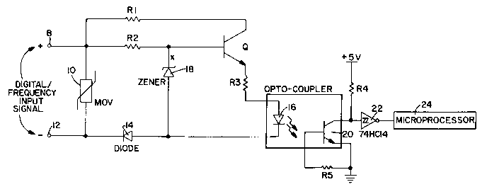
Fig. 1 is a schematic diagram of the input
circuit according to the present invention;
Fig. 2 is a waveform diagram showing the waveform
of a possible input control signal at the top, and the
waveform of a respective signal at the bottom, which has
been conditioned by the input circuit for use by a micro-
processor or other industrial control apparatus;
Fig. 3 is a view similar to Fig. 2 showing
another input control signal;
Fig. 4 is a view similar to Fig. 2 showing a
still further input control signal; and
Fig. 5 is a view similar to Fig. 2 showing a
possible non-standard input control signal.
DESCRIPTION OF THE PREFERRED EMBODIMENT
Referring to the drawings in particular, the
invention embodied therein comprises a control circuit for
receiving and conditioning input control signals having a
wide variety of waveform and voltage, and for supplying the
signals to a micro-processor or other industrial control
apparatus.
The invention provides an improved
digital/frequency input which is designed for industrial
control applications. A circuit diagram of the invention
is shown in Fig. 1.
200279 1
-- 4
The circuit allows a wide range of standard and
non-standard control signals to be applied. When tested,
it had a minimum high level threshold voltage of 11 volts
and a low level maximum of 8 volts for a zero to 10 KHz
signal. The circuit is capable of withstanding an input
voltage of 130 VDC and 250 VAC. Therefore, it can handle
any DC control signals from about 15 volts to 130 volts and
AC control signals from about 15 volts to 250 volts. Some
of the standard control input signals this will take are 15
10 VDC, 24 VDC, 28 VDC, 125 VDC, 24 VAC, 117 VAC, and 230 VAC.
All of these signals can be applied without the need of
jumpers to select the range. The only criteria for the
input signal is that it is above 15 volts for high level
and below 2 volts for low level while at the same time not
exceeding +130 VDC, 250 VAC or going negative more than -
350 VDC. The signal frequency limit was tested up to about
45 KHz; however, 10 KHz is good enough for most of the
control signal applications. Therefore, practically any
waveform shape that holds to this criteria may be used
successfully.
Some examples of possible waveforms are shown in
Figs. 2 to 5. Some waveform types that can be used are
square, triangle, and sinusoidal.
Returning now to Fig. 1, the circuit includes a
MOV (metal oxide varistor) 10 on the input terminals 8 and
12, which suppresses transients that appear over 370 volts.
A diode 14 allows positively biased signals to pass and
cuts off negatively biased signals. In the reverse bias
mode hardly any current flows which saves power and the
rest of the components. AS the signal is applied
positively to activate the high level, transistor Q turns
on which allows current through an opto-coupler diode 16.
The transistor Q and a zener diode 18 have bias currents
supplied from the signal through resistor R2. Once the
zener voltage is reached, it controls a steady current
through Q. This is due to the nearly constant voltage
200279 1
appearing across an output resistor R3. Therefore, after
the signal reaches this point it will only draw 3 to 4 mA
regardless of how much higher the signal goes.
This current through the opto-coupler diode 16
will cause the opto-coupler transistor 20 to conduct
thereby pulling the input to a 74HC14 inverter with Schmitt
trigger 22, low. The 74HC14 has a Schmitt trigger input
which provides the hysteresis necessary to keep noise from
causing false pulses. The inverted output of the 74HC14 is
taken to an input pin of a micro-processor 24 which uses
the signal for some industrial control function.
As the applied control signal drops, it will
reach a point where the current through R3 and the opto-
coupler 16, 20 is such that it allows the pull-up resistor
R4 to raise the input voltage to the 74HC14 which causes
the inverter output to go low. The micro-processor can
sense these changes in levels (edge triggered interrupts).
These interrupts can mark time by keeping track of the
counts between them. Since there is a known internal clock
frequency, one can determine the interrupt frequency. In a
DC digital control input situation, one can determine if
the level is high or low from reading the port or by
keeping track of the transition state.
AC line digital control input signals can be
realized by using the frequency mode. An AC line signal
can be recognized as a 45 to 65 Hz frequency for the high
level signal and less than this for a low level signal.
For 50/50 duty cycle waveforms, the frequency can be
determined in half of a cycle. Another approach for
determining the frequency is to count the transitions in a
fixed period of time, however, this will not give quick
results.
In Fig. 1, resistor R1 is connected between the
positive input terminal 8 and the collector of transistor
-
- 6 ~ 2 00279l
Q, for protecting the collector against surged current.
Resistor R5 is connected between the base and emitter of
the opto-coupler transistor 20 for reducing noise, and for
evening out opto-coupler on-off switching times.
The opto-coupler 16, 20 can, for example, be a
4N36, which is generally available in the industry.
Micro-processor 24 requires a 0-5V digital signal
to sense the input control signal and provide adequate
control to devices connected to the micro-processor.
The MOV 10 prevents transients and noise spikes
while the zener 18 sets the voltage for transistor Q, which
requires a control voltage to operate and itself set up a
constant current to the opto-coupler.
The improved digital/frequency input of the
invention has many advantages over prior methods.
The elimination of physical jumpers in the
circuit eliminates the need for a customer to set the
jumpers. Not only does this free the customer from going
through documentation on jumper positions, but it helps
prevent failure due to incorrect jumper settings.
Since the inventive circuit is practically
waveform independent, this gives the customer the
flexibility of running sinusoidal signals, square wave (on-
off DC signals), or non-standard signals such as a
triangular, if so desired.
Since this circuit doubles as a digital and/or
frequency input, additional circuitry such as frequency-to-
voltage converters or AC coupled configurations are not
required.
The circuit limits the current input to 3 to 4
X
7 - 200279l
mA which greatly reduces power consumption when high
voltages are applied. For instance, if the voltage applied
increased from 24VDC to 125VDC, then the power in a
standard resistive input circuit would go up by over 27
times what it started at; whereas, the improved circuit
only goes up by a factor of about 5.
This circuit typically pulls 3 to 4 mA. It
requires a minimum current to activate the high level
state; thus, this will provide some inherent noise
immunity. The 74HC14 with its Schmitt trigger input builds
in hysteresis which helps prevent output oscillation during
level transitions. The resistor R5 helps reduce noise from
activating the opto-coupler.
This invention can be applied to a variety of
input ranges and sensitivity level by changing the values
of R1, R2, R3 and the zener voltage. This would redefine
the threshold voltages and input current limiting values.
While a specific embodiment of the invention has
been shown and described in detail to illustrate the
application of the principles of the invention, it will be
understood that the invention may be embodied otherwise
without departing from such principles.