Note: Descriptions are shown in the official language in which they were submitted.
. 7515
-- 2Q03082 ~
ELECTRONIC FLASH CAMERA HAVING REDUCED CYCLE TIME
BAcKGRouND OF THE INVENTION
1. Field of the Invention
-
The present invention relates to a photographic
camera of the self-developing type having an electronic
5 flash, in general, and to such a camera having means for :~
reducing the overall cycle time of such a camera, in
particular.
2. Description of the Prior Art
Automatic photographic cameras of the
self-developing type such as those sold by Polaroid
Corporation of Cambridge, Massachusetts, under its
registered trademark "Impulse" are well known in the ~ -
art. These cameras are intended to be used with film
- cassettes containing a plurality of self-developlng film
units together with a battery which supplies electrical
energy for the operation of certain camera systems whose
functions, in part, are to expose and process a film
unit. These cameras may, for example, include an ex-
posure control system, a motor powered film transport
system for transporting and processing an exposed film
unit and electronic logic circuits that provide a
sequence control of such camera systems. In addition,
these cameras are adapted for use with an electronic
flash that is powered from the same film cassette battery
in a manner similar to that described in U.S. Patent No.
. 4,074,295 to R. C. Kee or in U.S. Patent No. 4,231,645 to
C. W. Davis, et al, both in common assignment herewith.
Heretofore, the simultaneous charging of an
electronic flash in a self-developing camera and the
,- : : - - , - :
.: .
.. .. .
.. ..
:: : :
``~ 2Q03082 '-
operation of an electrical subsystem that causes a heavy
power drain of the camera's battery, such as the opera-
tion of the motor that powers the film unit transport
system mentioned above, was avoided. Such simultaneous
charging and motor operation would consume large amounts
of power and thereby may reduce the battery's output
voltage below a level where it could properly drive the
motor for film processing purposes, i the power con-
sumption continued for an extended period of time.
Therefore, the operation of the film transport and pro-
cessing motor and the charging of the electronic flash
was sequentially timed so as not to occur simultaneous-
ly. This sequential type of electronic flash charging
and motor control is fully described in U.S. Patent No.
3,846,812 to C. H. Biber, in common assignment herewith.
In the camera described in this just-mentioned patent,
once an exposed film unit has been transported for
processing and ejected from the camera, the electronic
flash is sequenced to charge in readiness for the next
succeeding photographic exposure operation. During the
time that the motor is being operated for film transpor-
tation and processing, charging of the electronic flash
is inhibited. In the above-noted "Impulse" camera, for
example, electronic flash charging is inhibited for
almost two seconds, which is approximately one-half
the total time required to fully charge the electronic
flash. The length of time that the charging of the elec-
tronic flsh is inhibited is an additional length of time
that a camera operator must wait before initiating the
next camera cycle, a length of time that may interfere
with the camera operator's ability to rapidly photograph
the next scene.
UMMARY OF TE~E INVENTION
It is a primary object of the present
invention, therefore, to reduce the overall exposure
. , .
20030a2
cyc~le: time~of a photographic camera system of t.he
self-developing type that includes an electronic flash.
It:is~a~further object of~the present invention
to reduce the overall~exposure cycle` time of~a~;~photo-
S gr~aphic~camera system of th~e~ se~l:f~-developi~ng:type~having
an e~lectronic~fl~ash:that is connected~to:~a~,common~'power
souroe~for~electronic~flash chargi~ng.~purposes~ without
: adversely~affect:ing the::operation~of:~other~power:¢~on-
~ suming~ camera~dev~ices~;that àre àls;o''s~lmu1tanéous1y
,'",~ 1,0 ~ eonnected to the~same~-common power~source.~
It:is another~ object~of~th`e~present invention
o~reduce t:he; overal~ :exposure~cycle~ `t~ime o;f a~photo- .
g:raphc came~ra system~of:~the self-de:veloping type having
an electronic~flash,~by~charg:ing~the ~e~lectron~ic flash
'15 ~ at ~the`same time that ,the~camera'~s~film~'unit transport
s9stem;is properly transporting an~expos~ed film`unit
~:`.,~:,:: :, ` ,~-du:r~ing:film processi:ng.~
Other~objec~ts,~features~aDd/or~àdvantages of
~ thé~prese~nt`invention'will be readi~ly::apparent from the
,C,''~ 20~ ;',fol~10wi~ng~deta~iled description of~;a pre~ferred:embodiment
' th~e:réof~when taken~in~conjunction`~with;~the accompanying
: d~r~awings~
In accordance with a pre:ferred embodiment of -
: thé:present invention, a photogra;phic camera system of
2'5 'the type that includes' an electronic fl~ash, a battery
fo.r supplying electrica~l power to~the camera and a motor
driven traDsport:~system that transports:~an exposed film
~"SP',`~ unit~during ilm processing is provided with control
means for simultaneously connecting the electronic flash
to the battery for electronic flash charging purposes
while the film unit transport motor properly transports
an exposed film unit for film processing in order to
~"~ reduce the overall exposure cycle time. The control
means maintains the electrical c:onnection between the
~: ~
~ : 35 battery and the electronic flash while the motor driven
; ~
` 3
.` :
- . . . . . ., , , :, .
`~ 200308Z
,
,
; transport system transports an exposed~film unit so long
as the voltage of the battery is equal to or greater than -~
~a~magnltùde~that~does~not interfere with the transport
~motor~'s ab~i~lity~to acceptably drive~the system so as to
~5 ~transpor~t an~exposed~fl~lm~unlt durlog film processing to
thereby reduce~th~e~overall exposure~t~ime of the camera
sys~tem.~ The~ove~rall~exposure cycle;~time starts~ wlth the
actuation~of;an~exposute initiating~bu~tton and~ends when
the~electr~onic~ flash~h~as;been~rech~arged to a~level where~-
10~ ~at~a~subsequent~e~xposure using the"~electronic fla~sh maYbe made~
BRIEF DESCRIPTION OF THE~DRAWINGS
Flg.~l~ls~a~perspective~view,~partly in sec-
tion, of a self-developing eIectronic f~lash camera that
lncorporates a preferred~embodiment of;~the exposure cycle
time reducing arrangement of the present invention.
Fig. 2~i~s a f~unctiona~l~block diagram of the
exposure control, len~s-focusing~and film~advancing
systems of the camer~a of drawlng~-Fig.~
Fig. 3A is~a functional block diagram and
schematic of the voltage converter~and control portion
of~the funotional block~diagram~o~ drawing Fig. 2.
Pig~.~3B is an enlarged~ampli~tude vs. time graph
o the electronic flash, charge-controlling square wave
signal shown in drawing Fig. 3A.
DESCRIPTION OF A PREFERRED EMBODIMENT
Re~ferring now to the drawings, and specifically
to Fig. 1, there is shown an electronic flash camera 10,
` ` o the self-developing type, incorporating a preferred
embodiment of the exposure cycle time reducing arrange-
ment of the preqent invention. The camera 10 is designed
for use with a self-developing film unit 12 similar to
those described in U.S. Patent No. 3,415,644 to Land, in
common assignment herewith, and specifically incorporated
herein by reference. The film unit 12 is packaged in a
-4-
'
:''~ , ' .;`''i;,'.",':',: : ' . , , ,. '. ';:
- . - - .
~ ~ -- 200308æ-
.
film cassette 14 shown in the cond~itlon assumed just
after the c:assette~l4 has been inserted into the camera
10. The~ca:ssette~14~further encloses,a 6 VDC:battery
6. The~batte~ry 16 supplies elec~t~r~cal energy for the
S~ :ope~ra~tion~of~:sev~era~ electrically~,operated camera'
s~ubsystems~and~components.~
Mounted~wi~thi~n~the camera~l:O~i~s a film~adva~nc- .,
ing.apparatus lS~:(Fig.~:2) s:imilar to~'~that:described in
~ U~.S.~ Patent No.~3,753,392.~to Land~tbàt~includes :a motor
,s ~ 10~ 8~for operati~ng~a~g~ear~train ~(not~;shown) which is
coupled wi~th the~filD~advanci~ng apparatus.IS~;to~provide
'for~the~continuous movement~of~an~é~xposè:d~fllm unit from .:
an exposure position withi~n :the~camera 10 toward the .:
exterior thereof.~The~film advancing~;apparatus 15 addi- ~
15~ tionally Includes a~.film-engag~ing~arm~member ~not shown) ''
dr~ive`n by:-the:motor-~1~8~and the abové:-mentioned~:gear
~ tr'ain~. The arm member is adapted~to~ex~tend~into~a slot- '.
;,'",~ : in'.thé casse~tte 14,~ as shown in the~above-noted Land '392
pa'tentl~ and engage ~the~uppermost~film un~it 1~2~at or near
2,0;,~its trailin~ edge~prior~to~moving~it out:~of:the cassette
4~an,d~into~the:bite of~a pair:~of~:~process~ing roi:lers 20
},"~ and ~22,~mounted adj~a:cent a leading~edge of the'film unit
?,-~ ,'12.~:The rotating~'processing~ rollers~20~a~nd 22, which are '.
driven.:by~:the motor:18 through~the~above-mentioned gear
25~ t~ra1n,,~continue the uninterrupted movement of the film
, unit~toward tbe~exterior of the~camera ~10 while simul-
~ , tanoously rupturing a container~of processing liquid at
'',.J',,~ the leading end of an exposed film unit. The processing
rollers 20 and 22 spread the liquid contents of the
ruptured container between photosensitive and image
réceiving elements of~the film unit to initiate formation
of a visible image within the film unit in a manner that
i8 well-known in the art.
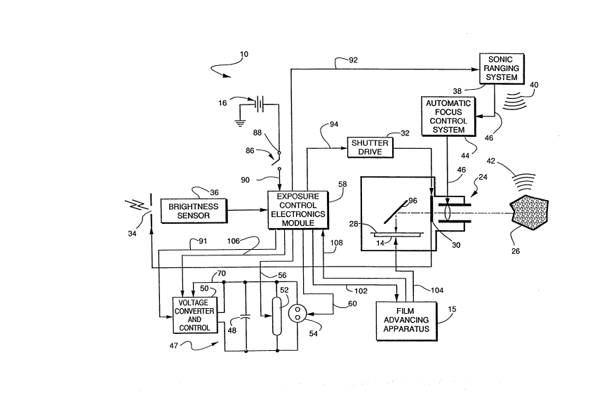
: With additional reference to Fig. 2 of the
, ~ ~
~ 35 ~ drawlngs, the camera 10 also includes an objective or
.
_5_
,: ,
, . ~, . . , . ~. . , , , . . ~ , , .
` 200308Z
taking lens 24 comprising a plurality of elements
retained in a spaced relation by a conventional cylin-
drical lens mount which may be adapted in a well-known
manner to provide translational movement of the elements
of the lens 24 along a central optical axis for focusing
image-carrying light rays of, for example, an object 26
on a film plane 28 of the camera 10 through an aperture
formed in a shutter mechanism 30.
The shutter mechanism 30, positioned inter-
10 mediate of the lens 24 and the film plane 28, includes a -
pair of overlapping shutter blade elements (not shown in
detail) of the "scanning" type. Scene light admitting
primary apertures (not shown) are provided in each of
the shutter blade elements to cooperatively define a
progressive variation of effective aperture openings in
accordance with simultaneous longitudinal and lateral
displacement of one blade element with respect to the
other blade element in a manner more fully described in
commonly assigned U.S. Patent No. 3,942,183 to Whiteside,
now specifically incorporated herein by reference. The
blade element apertures are selectively shaped so as to
overlap the central optical axis of the lens 24 thereby
defining a gradually varying effective aperture size as
a function of the position of the blade elements of the
shutter assembly 30. A shutter drive 32 is provided for
displacing the shutter blade elements of the shutter
mechanism 30. The shutter drive 32 includes a tractive
electromagnetic device in the form of a solenoid (not
shown) employed to displace the shutter blade elements
with respect to one another in a manner more fully
described in the above-noted Whiteside patent.
Each of the shutter blade elements additionally
includes a secondary aperture (not shown in detail) with
an aperture in one blade element cooperating with an
aperture in another blade element to form an opening 34
200308Z
therethrough. Thes~e secondary~apertures may be qon- -
figured to track in~a predeterm~ined corrèspondin~
relationshlp wLth~the;scene light~ admi~tting ~pr~lmary
: : apertures (not shown)~within the~s~hutt~er~me~chan;ism 30.
5 ~With ~the~primary~and~secondary~ape~rtures~being~formed in
""~ the~,~same~blade~el~ement~and~there~fore~being~mèchanically
coupled' to one anothe~r,~it is~readily~appare~nt~that the
sè~c,onda~ry~aperturea~move~in~the~;s~e~manner~as~the pri-
~S~ ;ma~r'y apertures.~ The~sècondary~àpe~r~tures~mQve~;in~the same
lO~direction~as the~primary~apertures when~con~troll;ing~scene
",~ light,~pàs~s~ing~through~thé sècondary-a~perture-ormed~open-
ing 34, tran~smitted~from a~scene belng photograph~ed,~to a
'photosens~itive;~element ~not s~hown~within~a~brlghtness
se:nsor ~36. An example of scanning~blade~elements having
,l5,~ ~;prim;ary~and secondary~apertures;~that~coop,erato to control ~,
th,é~amount of scene light admitted~to~a~;single photosen-
si~tive element i9~ shown in U.S.~Patent~No,.~3;,942,183,
s~upra.~
'",''~ ; The~photographic~came,ra`lO~is~ prov~ided with a
Z'O'~;,s,;nic~rangln ~sys~tem~38~that~ln ~l~es~a~ra ging~¢lrcuit
, an,d~,aa~'ul~tr'asonlc~transducer~(~neither~shown~)~h~lch may be'
'a,c-tua'ted;to transmit a burst of sonic energy 40 toward a
' sab,~ ct to~be~photographed, such~;às~the subject~26. The
,~,','',',~;~`,'~ ~ trans'ducer'thereafter operates to detect an echo 42 of
o 25~ ~,thé,'b~urst of~sonic energy reflected~from~the sub~ect 26.
,,","~ Th-~total round-trip time for a;~bùrst of~sonic energy
,to,~be transmi,ttéd~ toward and for~a~n echo thereof to
be,'reflected from the subject 26 and detected by the
'' ;tra~nsducer of the sonic ranging,system~38 is a fa-irly
' 3'0 accurate measure of camera-to-subject distance. An
" electrical signal representative of this round-trip time
is subse~quently employed to focus~the adjustable~focus
lens' 24. U.S. Patent No. 4,199,246 to Muggli describes
such a sonic rangefinder in much~greater detail. An
automatic focus control system 44, coupled to the
7-
i
"~ ~:
-- 2003082 '
,
adjustable focus lens 24 through a path 45, causes the
lens 24 to focus an image of the.subject 26 onto the film
plane 28 of the camera 10 during an exposure, in response
to an electrical subject distance related signal from the
sonic ranging system 38 through a path 46. An example of
an automatic focus control system functioning in this
manner is more fully described in U.S. Patent No.
4,199,244 to Shenk.
The camera 10 is also provided with an elec-
tronic flash apparatus 47 together with apparatus forcontrolling its energization, to provide a portion of
the exposure value required to illuminate a scene to
be photographed. The electronic flash apparatus 47 com-
prises a main storage capacitor 48 which may be charged
up to an operating voltage by a voltage converter and
control 50. The design and operating characteristics of
the voltage converter and control 50 will be described
below in detail. In general, voltage converter and
control 50 operates to convert a dc voltage as may be
derived from the 6 VDC battery 16 contained within the
cassette 14, to a suitable operating voltage such as 350
VDC. A flash tube 52 and a quench tube 54 are connected
in a parallel relation with respect to the main storage
capacitor 48. The flash tube 52 may be energized by a
suitable trigger signal on a path 56 from a conventional
trigger circuit (not shown) within an exposure control
electronics module 58, and the quench tube 54 may be
ignited by a suitable trigger signal on a path 60 from
another conventional trigger circuit (not shown) that
is also included within the exposure control electronics
module 58.
As noted above, the camera 10 includes the film
advancing apparatus 15 for the continuous movement of an
exposed film unit from an exposure position within the
camera lO toward the exterior thereof. The rollers 20
.. .
- : . ,
,,
,...... . , , ,,:
,
` ` 2003082
, ,
and 22 driven by the motor 18 of the film advancing
apparatus l5 rupture a container of processing liquid at
the leading end of an exposed film unit and then spread
its contents between photosensitive and image receiving
film elements on layers thereof to initiate the formation
of a visible image. In order to produce an image having
the desired resolution and sensitometric characteristics,
it is essential that the layer of processing liquid that
is spread between the film elements by the spread rollers
20 and 22 be of a uniform and predetermined thickness.
This type of processing liquid layer thickness is pro-
duced, in part, by driving the rollers 20 and 22 at a
fairly constant and predetermined rate of speed. A
roller speed in excess of this predetermined rate will
cause the spreading of an excessively thick layer of
processing liquid between the film elements, whereas a
roller spread below this predetermined rate will cause
the spreading of an excessively thin layer of processing
liquid between the film elements.
Inasmuch as the rollers 20 and 22 are driven
by the motor 18, maintaining the rotational speed of the
motor 18 within certain limits will result in the proper
rotational speed of the rollers 20 and 22 and therefore
the proper spreading of a layer of processing liquid
between the film elements. The rotational speed of the
motor 18 can readily be maintained within the desired
limits if the voltage level of the power source supply-
ing electrical energy to the motor 18, such as the 6 VDC
battery 16 within the cassette 14, is maintained within
certain voltage limits. However, if a large current
drain producing load is connected to a common power
source such as the battery 16 at the same time that the
battery 16 is supplying electrical power to the film
advancing apparatus 15, such as the charging circuitry
within the electronic flash apparatus 47, the converter
`,-
: : . .
, . : -:
` 20030l32~
and control 50 that charges the main storage capacitor 48
will place a substantial current drain on the battery
16. This level of power consumption will ultimately
reduce the level of voltage available from the battery
16. With the film advancing apparatus being operated
at the same time that the electronic flash apparatus 47
is being charged, the voltage available from the common
power source or battery 16 will ultimately drop below
the minimum level required to maintain the motor 18 and
therefore the rollers 20 and 22 coupled thereto at a
rotational speed necessary to produce a photographic
image having the desired resolution and sensitometric
characteristics mentioned above.
In the past this problem was avoided by inhib
iting the operation of the charging cicuitry within the
electronic flash apparatus until movement of an exposed
film unit by the film advancing apparatus for film pro-
cessing and for movement out of a self-developing camera
was complete. The amount of inhibit time as a function
of the total electronic flash charging time in a self-
developing camera was considerable. For example, it
ta~es approximately 4 seconds to charge the electronic
flash aparatus in one type of self-developing camera when
the main storage capacitor in the electronic flash appa-
ratus is fully discharged. The film advancing apparatustakes approximately 2 seconds to move an exposed film
unit from its exposure position to the exterior of the
camera. Charging of the electronic flash apparatus was
delayed for this entire 2 second interval which amounts
to 50 percent of the total charging time required to
ully charge the electronic flash. As a consequence,
the exposure cycle time, which is defined herein as
the length of time required between the actuation of a
camera's shutter button by a camera operator to initiate
an exposure cycle and the time that the electronic flash
--10--
:: - . '~ " ,.
: . . . : .. : . . .. ..
- - . , - :
-
.
.
` -- 20~308Z'_-
is fully charged and is ready for the next exposure, is
lengthened by this 2 second interval of time. A camera
operator may, for example, miss an opportunity to photo-
graph a particular scene if the subject matter of the
scene is only available during this 2 second time in-
terval. The present arrangement avoids this problem
by sensing the battery voltage and then enabling the
charging of the elecronic flash during the operation of
the film advancing apparatus 15, in a particular manner,
only when the battery voltage does not drop below a
minimum voltage level where it would interfere with its
ability to maintain the proper rotational speed of the
film advancing apparatus drive motor 18. A circuit for
controlling the charging of the electronic flash appa-
ratus 47 as a function of the voltage provided to thecamera 10 by the battery 16 when its output voltage is
equal to or exceeds the above-mentioned minimum voltage
level is shown in drawing Fig. 3A.
In Fig. 3A, there is shown a schematic diagram
of the voltage converter and control 50 of the camera
10. The voltage converter and control 50 includes a
voltage step-up transformer 62 whose primary coil is in
series with switch means that includes a transistor 64,
and the battery 16. An oscillator control system 66 is
also included within the voltage converter and control
50. When energized, oscillator control system 66 gen-
erates a square wave output signal 68 at a frequency of
approximately 20 kilohertz. This output signal is
applied to the base of the transistor 64 which, in turn,
causes the power from the battery 16 to be applied to the
primary of the voltage step-up transformer 62 at this 20
kilohertz frequency. This varying power that is applied
to the primary of the transformer 62 is converted from
a level of approximatley 6 VDC to a working level of
approximately 350 VDC. The converted power at this
, -
-. ., -:
" '' ~ , . :. :
20030F'~
350 VDC voltage level is then employed to charge the
electrical energy storing main storage capacitor 48
which is connected to a secondary coil of the trans-
former 62 through a voltage rectifying diode. Circuitry
(not shown) within the oscillator control 66 senses the
voltage level on the main storage capacitor 48 through a
path 70. When the voltage on the capacitor 48 reaches a
predetermined magnitude, the above-noted circuitry termi-
nates the square wave output of the oscillator control
system 66 and therefore the charging of the main storage
capacitor 48.
Voltage sense and comparator 72 senses the
output voltage of the battery 16 and then utilizes a
comparator (not shown) to determine whether or not the
sensed voltage is equal to or greater than a predeter-
mined magnitude. This predetermined magnitude is the
minimum voltage that will properly operate the drive
motor 18 to transport an exposed film unit during film
processing. The output of the voltage sense and compara-
tor 72 is applied to a charge control algorithm 74 whichcontrols the rate at which the oscillator control system
66 causes the main storage capacitor 48 to be charged.
The charging rate of the main storage capacitor 48 is
controlled by maintaining the square wave output signal
68 at a fixed 20 kilohertz frequency and varying the
width of each portion of the square wave that turns on
the transistor 64. An enlarged representation of a
portion of the square wave signal 68 generated by the
oscillator control system 66 is shown in drawing Fig. 3B.
With additional reference to Fig. 3B, square
wave signal 68 having a frequency of 20 kilohertz regu-
larly varies in magnitude from a minimum voltage level 76
wherein the transistor 64 is in its off or non-conducting
state, to a maximum voltage level 77 where the transistor
64 is placed in its on or conducting state. In this
-12-
:, , , , :, ' , ,
' ~
- ~ 200~082 ~
particular transistor 64 switching arrangement and under
conditions where the output voltage of the battery 16 is
a~ or near its maximum output level, the length of time
78 that the square wave signal 68 is at its maximum level
77 is approximately equal to the length of time 80 that
this signal is at its mimimum level 76. As a conse-
quence, under such conditions the on and off times of the
transistor 64 are approximately equal. As the difference
between the output voltage of the battery 16 and the
10 minimum voltage required to properly operate the drive ;
motor 18 during film processing decreases, as determined
by the voltage sense and comparator 72, the charge con-
trol algorithm 74 causes the pulse width or on time 78
and the off time 80 of the square wave signal 68 to
decrease and increase, respectively, in response to this
decreasing voltage diference. As an example, and as
shown in Fig. 3B, the pulse width on time of the square
wave signal 68 may be reduced to the time interval 82 at
a particular level of the battery 16 voltage, whereas the
off time, which constitutes the remainder of a square
wave cycle, would concurrently be increased to the time
interval 84. When the output voltage of the battery 16
is less than the minimum voltage required to properly
operate the drive motor 18 during film processing, the
on time of the square wave signal 68 would be zero and,
therefore~ as will be explained below, no further
charging of the electronic flash apparatus 47 would be
allowed to occur during this low voltage condition while
the motor 18 is driving the film advancing apparatus 15
during film transport and processing.
OPERATION
A typical exposure cycle that includes the
simultaneous charging of the electronic flash apparatus
47 and the operation of the drive motor 18 during film
processing will now be described in detail. For the
-13-
.
. . .
~_ 2003082~
purpose of this description, it i9 assumed that the out-
put voltage of the battery 16 is at or near its maximum
level and that the flash apparatus 47 is fully charged.
With reference to Figs. 1 and 2 of the drawings, a switch
86 is actuated to its closed position by a camera oper-
ator to initiate an exposure cycle. The closure of the
switch 86 couples the battery 16, which is connected to
a terminal 88, to the exposure control electronics module
58 through a path 90 and then to the voltage converter
and control S0 through the exposure control electronics
module 58 and the path 91. The exposure control elec-
tronics module 58, in turn, actuates the sonar ranging
system 38 through a path 92 to derive a subject 26 to
camera 10 distance signal which is then employed by the
focus control system 44 to adjust the lens 24 to the
correct focus position. The exposure control electronics
module 58 also actuates the shutter drive 32 through a
path 94 to thereby drive the shutter mechanism 30 to
generate an exposure interval in a conventional manner
so that an image of the subject 26 may be reflected by a
mirror 96 and formed on the film plane 28 of the camera
10 by the lens 24 in conformance with the level of scene
light as determined by the brightness sensor 36.
During the exposure interval, the flashtube 52
and the quenchtube 54 are ignited by the exposure control
electronics module 58 to produce the required amount of
supplemental scene illumination in the above-described
manner, also in conformance with the level of scene light
that is sensed by the brightness sensor 36. At the com-
pletion of the exposure interval, the exposure controlelectronics module 58 actuates the film advancing appa-
ratus 15 and the drive motor 18 included therein, through
a path 102, to initiate the transport and film processing
of an exposed film unit. The film advancing apparatus
lS, in turn, moves the exposed film unit, located in the
-14-
^~ 2003082
cassette 14, through the path 104, into the bite of the
rollers 20 and 22, and then drives the rollers, in the
manner described above, to spread processing liquid
between certain film unit layers and to move the exposed
film unit into an exit slot 106 (Fig. 1) in the housing
of the self-developing camera 10.
At the same time that the film advancing appa-
ratus 15 is actuated to initiate the transport and pro-
cessing of an exposed film unit, the oscillator;control
system 66 within the voltage converter and control 50
is actuated to initiate~the charging of the main storage
capacitor 48 of the electronic flash apparatus 47 through
a path 106. The simultaneous operation of the drive
motor 18 within the film advancing apparatus lS and the
charging of the electronic flash apparatus 47 will con-
tinue, in the above-described manner, until the main
storage capacitor 48 is fully charged, only as long as
the output voltage of the bat~ery 16 does not drop below
a level that would interfere with the ability of the
drive motor 18 to properly drive the film advancing
apparatus 15 during film transport and processing.
As noted above, voltage sense and comparator
72 determines when this low level of voltage occurs and
then causes the charge control algorithm 74 to terminate
the charging of the main storage capacitor 48 by the
oscillator control system 66 for as long as this condi-
tion persists. The voltage on the main storage capacitor
48, which is a direct measure of its charge level, is
monitored by the oscillator control system 66 through
the path 70, as previously noted. If the main storage
capacitor 48 is not fully charged before its charging
has been terminated due to an excessively low level of
battery 16 output voltage, capacitor 48 charging will
continue until it is fully charged after operation of the
film advancing apparatus 15 is complete. Completion of
--15--
,. . : ,: ..,,.:. ~ , :~
- .. , ., . :
2C03082
.
the film advancing apparatus 15 cycle is monitored by the
exposure control electronics module through a path 108.
When the film advancing apparatus 15 cycle is complete,
the exposure control electronics module 58 once again
initiates charging of the main storage capacitor 48 by
the oscillator control system 66 with a charge initiation
signal through the path 106 which temporarily overrides
the control of the oscillator control system 66 by the
charge control algorithm 74 until the capacitor 48, as
sensed through the path 70, is fully charged. The end
of the exposure cycle, as that term is employed herein,
occurs when the main storage capacitor is fully charged
and is ready to supply electrical energy to the flashtube
52 for the next exposure. By initiating the charging of
the electronic flash apparatus 47 at the same time that
- the film advancing apparatus 15 is transporting and
processing an exposed film unit, the total time required
to complete an exposure cycle is substantially reduced.
Even in those instances where electronic flash charging
must be interrupted during the operation of the film
advancing apparatus 15 due to low battery voltage, the
additional time required to fully charge the main storage
capacitor 48, when added to the time required to operate
the film advancing apparatus 15, will almost always be
less than the time that would otherwise be required if
the charging of the electronic flash apparatus 47 was
delayed until the operation of the film advancing
apparatus 15 was complete.
From the foregoing description of the invention,
it will be apparent to those skilled in the art that
various improvements and modifications can be made in it
without departing from its true scope. The embodiments
described herein are merely illustrative and should not
be viewed as the only embodiments that might encompass
the invention.
-16-