Note: Descriptions are shown in the official language in which they were submitted.
20031~1
Tlle pl esent invention eliltes to a universal micro circuit for use in digital signal llrocessing,
f`or example fomstoring ancl translllitting information in a telecommunication system.
In present day known technology, a number of circuits intended for relatively low data speeds
are used to solve certain application problems. Normally, a large number of circuits are
needed for one single application.
Problerlls which arise in known techniques are, for instance, the large number of internal
connections resulting from a large number of circuits, the difficulties in achieving short cycle
times when the circuits are spaced far apart, the high power consumption, and the Llrge
number of connecting pins that are involved. When taken together, these problems create
high demands on space.
According to the present invention there is provided an integrated micro-circuit for use in
digital signal processing, for example for storing and transmitting information in a
telecommunication system, particularly digital information between switch modules in a
telephone exchange, achieving, in a small physical space, high packing density, short
propagation times, low power consumption and a small number of internal connections on a
superior system level, said integrated micro-circuit comprising a single silicon substrate
having input and output connection units in the form of pads for establishing connections
between the integrated circuit and various types of external units connected to said
integrated circuit, said connection units being of two types, namely a first type an(l a second
type; said first type of connection unit adapting the integrated circuit to an interface for
transmission of data at high to very high data speeds, and said second type of connection unit
adapting the integrated circuit to normal standard logic for normal to low data speed; said
circuit further including a logic unit comprising a gate-matrix network for implementing
various logic functions, a memory comprising a pluraiity of full custom designed memory
rnodules which when necessary can be varied to the number and furthermore combined to
fulfil the requirement of memory capacity for each separate application; a control unit for
controlling the writing and reading of data into and out of the memories, at least one time-
slot counter, and a synchronizing logic unit for the transmission of synchronizing signals to
the units on the circuit; and the proportion of the silicon-substrate area for the memory being
considerably greater than the proportion of the surface for the gate matrL~; and a bit
synchronizing module common to a plurality of incoming data flows is placed on the silicon
substrate to allow dynamic phase variations between data and clock in~ormation without loss
of data.
20031;~
The ~rrnn ement according to the present invelltioll solves the aforesaid problems by hlrge
scale integrlltion of different ~unctions on a single chip (silicon substrate).
There are few connections between silicon chips on a printed circuit board, but many internal
connections on a silicon chip, since it is about 100 times cheaper to make the connections on
the chip than on the printed circuit board. 1'his chip is a VLSI circuit (Very Large Scale
Tntegration) intended for a number of mutually different telecommunication applications.
The circuit consists of a number of read/write memory unils and a gate-matrix area for
forming standard random logic. The circuit also includes input/output buffers (I/0) which
enable communication to take place over a modified CCITI standard interface, called IVC4
(Internal Virtual Container, Level 4). In the case of this internal interface, information is
transmitted between switching modules in a larger switch in a telecommunications system
having a speed of 163.84 Mbit/s, hereinafter referred to as the 164 Mbit/s. Also included in
the 164 Mbit/s-frame is an internal-switch overhead of 130 bytes, which is included in order
to make control signalling and switch operation possible.
The inventive arrangèment solves the aforesaid problems, by incorporating a large number of
memory banks and a gate-matrix area on one single chip, where the memory proportion is
considerably larger than the gate-matrix proportion.
The advantages afforded hereby are:
- short cycle times
- few connections
- low power consumption
- low costs for capsules and printed boards
The inventive arrangement is described below with reference to an exemplifying embodiment
thereof and with reference to the accompanying drawings, in which
Figure 1 is a simple illustration of the function of known technique;
Figure 2 illustrates the integration method;
Figure 3 illustrates the manner of constructing a chip in accordance with the invention;
Figure 4 illustrates a iime switch stage incorporating the inventive arrangement; and
Figure 5 illustrates a space switch stage incorporating the inventive arrangement.
The characteristic differences between telephone exchange applications and large computer
applications are:
- That the useful life telephone exchanges is from between 20 to 50 years, whereas the useful
life of large computers is only about 5 years.
200312~
- The circumstances of ambient temperature requirements are also quite
different. The ambient temperature in the case of large computers is 20+ 1 C.
Telephone stations, on the other hand, must be capable of managing variations
in ambient temperature of from +5 to +50 C. This places high demands on the
semiconductor process in telephone exchange applications. A very important
requirement is one of low power consumption, which in turn results in low
silicon-chip temperature, resulting in low error intensity and long useful life.The transportation of data in telephone exchanges can be very intensive. The
inputs and outputs on a chip constructed in accordance with the invention can
be configured to transmit information at either low or high speeds.
The low-speed alternative requires the provision of a large number of connec-
tions to the capsule, which results in high capsule and silicon costs. The circuit
boards in which these capsules, which comprise a very large number of pins, are
to be mounted require a fine pattern class and many layers, and consequently
the circuit boards are also expensive.
The high-speed alternative results in fewer connections to the capsule, cheaper
capsules, cheaper silicon chips and cheaper circuit boards.
The high speed on the inputs and outputs however, places certain requirements,
for instance high ft (limit frequency) on the bipolar transistors and low parasite
capacitance in order to achieve low power consumption.
Figure 1 illustrates a known technique in the form of an external memory
SRAM (Static Random Access Memory) which operates towards a large number
of application-specific integrated circuits, ASIC:s. It is very difficult to achieve
short cycle times with such a solution. This is because the application-specificcircuit includes a register containing the address to the SRAM memory. The
address is transmitted via the output unit (pad) of the ASIC circuit through thecircuit board on which the circuits are mounted, into the address inputs of the
SRAM memory, so that data is pointed out and read from the correct position in
the memory SRAM. The data information is then transported through the
circuit board into the application-specific circuit, and into the register via the
input units. This results in a very high overhead in relation to the access time of
the memory, which means that the total cycle time will be twice that of the
memory access time.
20D3~2~
Furthermore, the external address and data flow results in a large number of
connections between the application-specific circuit and the memory SRAM,
which in turn results in high power generation and an expensive circuit board.
The inventive arrangement solves these problems, by integrating the memory
function and the gate-matrix function for the same silicon plate on a single
chip, as illustrated in Figure 2. The advantages afforded hereby are:
- Short cycle times as proposed to SRAM, as a result of the integration on said
chip.
- Fewer number of connections on the capsule, partly as a result of the
integration of the SRAM memory, and partly as a result of the high input-
output speed. The speed on input/outputs coincides with the speed on external
terminals to telephone exchanges, the speed of which has been increased to 155
Mb/s and in the future will be increased conceivably to 620 Mb/s. This is
another reason for the high input/output speed to/from the chip according to
the invention.
- The aforesaid also results in low power consumption and much lower costs for
capsules, silicon chips and circuit board.
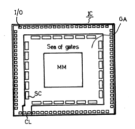
As will be seen from Figure 3, a chip constructed in accordance with the
invention comprises three parts, i.e. an input/output part, a logic part and a
memory part.
The input/output part comprises a plurality of pads I/O for connection betwee
the chip and the various external connecting units. The chip presents, for
instance, a first type of input/output units for adaptation to high speeds of low
voltage swing and low power cons~mption. Another type of pads adapt to TTL
logic and are intended for communication with standard logic and micro-
processors of low speed. A third type of unit connects to earth, and fourth typeof unit connects to different supply voltages. The units referenced CL are
inputs for clock signals. The units SC are synchronizers and series/parallel/pa-rallel/series converters.
200312~
The logic part comprises a gate-matrix area GA which includes 17,000 gate
functions. It is possible to implement a large number of logic funtions in this
gate matrix, depending upon the application. In the case of the illustrated
embodiment, the basic elements of the gate matrix are NAND gates. The
memory part consists of a 160 kb memory capacity in the form of 64 memory
modules MM each having 640 word of 4 bits, which can be configured to a
broader memory word and a greater memory depth if so desired. It is also
possible to vary the number of memory modules within the framework of the
total memory capacity and the space on the silicon plate.
The proportion of memory area in relation to the proportion of gate-matrix
area on the chip is about 3/4 memory and 1/4 gate matrix.
The connection between memory modules and gate-matrix logic is effected
through metallizations on the silicon plate. The gate-matrix function is selected
by interconnecting NAND gates in a desired configuration with the aid of such
metallizations. The third function of the metallization is to constitute a
connection between input/output units I/O and the gate matrix. The function of
these input/output units can also be programmed with the aid of metallizations.
In the case of the illustrated embodiment, the memory modules and gate
matries are built-up on a chip with the aid of eleven mutually common mask
layers. Seven unique mask layers connect gate matrices with memory modules
and input/output units.
The inventive circuit can be utilized in a large number of mutually different
applications, for example:
- Different types of buffer memory
- Queue memory (linked list)
- Mioroprogram memory for execution of instructions
- Elastic buffer for equalizing phase differences
- FIFO
Further examples of such areas of use include the incorporation of the circuit in
TS switches (Time-Space), concentrators, terminal units ~ET) for telephone
2003~;21
stations, digital multiplexors, etc. One very important application, an account
of which is given below, is the use of the circuit as a switch memory, for
example in a digital switch of the TST type (Time-Space-Time) in a telephone
exchange. Since the principle of time division is known, it will not be described
here.
The larger part of such a digital switch can be implemented by utilizing the
inventive chip in two applications:
- The time-stage chip tTsC) which performs the necessary time-switching
functions to the 164 Mb/s line (IVC4) in both directions. All the time memories
are duplicated, to avoid congestions In the T-S-T structure, see Figure 4.
- The space-stage chip (SSC) which performs the synchronous space switching,
see Figure 5.
As will be seen from Figure 4, the time switch comprlses two stages, an
incoming time stage and an outgoing time stage.
A common feature of the two stages is a control unit SNC (Switchlng Network
Controller) implemented in the gate-matrix network in the form of a micro-
prograrnmed processor, which i5 realized with the aid of circuits from the
family AMD 29XX. The purpose of the control unit is to read status information
from and write control information in the control memorie CS present on the
chip. The control unit SNC has a clock input, a frame-synchronizing input 8 kHz
and data inputs and outputs for communication with the next higher control-
system level.
The data flow of 164 Mbit/s entering the time stage comes from external
devices connected to the switch and is delivered to two switch memories SS. In
the case of the illustrated embodiment, each of these switch memories has a
format of 640 words each of 8 bits, of which 288 words are used for column
switching. Data is written into the memory in parallel form. Writing of the
incoming bit flow into the memories is controlled by a time slot counter TC
incorporated in the gate matrix. Identical information is written into both
memories.
2003121
The function of the control memories CS is to control the reading and writing
of data in corresponding switch memories SS. The control memories have a
format of 640 words of 12 bits each, of which 288 words and 9 bits are used.
Data is read from and written into said control memories in parallel form. Data
which is read from said switch memories SS has an 8-bit format. The
information read frorn the memory is converted from parallel to series format
and transmitted to the space stage SSC at a speed of 164 Mbit/s. Parallel/seriesconverters and series/parallel converters are implemented in the gate-matrix
area ~A. As will be seen from the figures, two arrays of switch memory and
control memory are provided. As before mentioned, this is because twice as
many internal time slots are desired, in order to avoid internal congestion in the
switch. In general, this means that the contents of the upper and the lower
control memory will not be mutually the same.
As will be seen from Figure 4, the outgoing time stage recelves on the differentinput of its~ connecting circuits two data flows transmitted from the space
stage, each of said flows having a speed of 164 Mbit/s. The data flows are sent
to respective switch memories SS. The switch memories have a format of 640
words of 8 bits, of which 288 words are used for switching columns. Data is
written into a switch memory while being controlled by the control memory CS
2~ co-acting with said memory. The control memory has a format of 640 words of12 bits each, of which 288 words and 9 bits are utilized for column switching.
One of the 288 positions in the switch memory is selected with the aid of the 9
bits in the corresponding control memory, i.e. the control memory controls the
writing of incoming data into one of the 288 positions of the switch memory.
The next incoming data is written into the switch memory, in a known manner,
during the next time slot in a frame comprised of a number of time slots. The
position in the switch memory is controlled by the content of the next-arriving
consecutive postion in the control memory. Reading of data from the switch
memory is eMective in a consecutive order and is controlled by a time slot
counter TC.
Subsequent to reading data from the switch memories SS, the two 164 Mbit/s
data flows are sent to the inputs of a multiplexer MX. The multiplexer seleots
words from solely one of the two data flows, while being controlled by a cuntrolmemory CS intrinsic to said multiplexer. Each word in the control memory
200312~
includes 4 bits. Only one of these is used for selection of multiplexer positions.
The new 164 Mbit/s data flow on the output of the multiplexer is converted
from parallel to series form and transmitted further to units connected to
switch matrices.
The space switch stage SSC illustrated in Figure 5 has the format 16 x 16. The
16 data flows of 164 Mbit/s sent from the incoming time stage to the space
switch are numbered û-15. The space switch contains 16 multiplexers MXO-
MX15, and one control memory CSO-C515 corresponding to said multiplexers.
Frame and word synchronization is effected by synchronizing logic FSL
implemented in the gate matrix.
The gate-matrix area incorporates a switching network marker SNC, a micro-
programmed processor of the aforementioned kind, the function of which is to
update the 16 control memories. The switching network marker includes a
clock-signal~input of 164 MHz, a frame synchronizing input of 8 kHz, and data
inputs and data outputs for communication with a superior control system.
The incoming data flow No. 0 is conneoted to position No. 0 on all sixteen
multiplexers. Data flow No. 1 is connected to position No. 1 on all sixteen
multiplexers, and so on for all of the sixteen data flows.
Consider multiplexer No. û which is connected to data flow No. 0. The
multiplexer is controlled by a control memory CSO having a format of 640
words each of 4 bits, whereof 288 words are used. Consequently, during a given
time slot of a frame, the multiplexer will be located in one of the sixteen
positions, this position being determined by the position of the control memory.The position of the multiplexer is controlled during the next time slot by the
next position in the control memory, and so on until all 288 positions have
passed through. The first position in the control memory is then read again. Theremaining 15 multiplexers and their associated control memories operate in the
same manner. The description does not include time-division principle or the
writing and reading of data into and from the memories, since such principles
and procedures are knwon to the art.