Note: Descriptions are shown in the official language in which they were submitted.
2003292
TITLE OF THE INVENTION
FLAT DISPLAY
FILED OF THE INVENTION
The present invention relates to devices for
displaying images by exciting phosphors on a display
panel with electron beams, and more particularly to flat
displays suitable for use in large-screen television
receivers.
BACXGROUND OF THE INVENTION
Research is conducted on flat displays having
a large screen for use as displays for high definition
television. CRTs generally in use as display devices
are most excellent in respect of the quality of images
since a high-speed electron beam is projected on phosphors
for excitation. However, high definition television
receivers of 40 inches or larger comprising such a
display device exceed 170 kg in weight and 850 mm in
depth and are not suited to household use.
Accordingly, U.S. Patent No. 4,719,388 or
Unexamined Japanese Patent Publication SHO 61-242489
disclosesa flat display of the electron beam type
which comprises linear filament cathodes serving as
electron beam emitters and in which the high-speed
electron beams derived by XY matrix electodes are adapted
!~, ,.,. . . ' ' . ' '
.' ' ' ~ '' ~ ' ' ' "' '
- ~ '
200329Z
impinge on specified addresses on a fluorescent screen.
Fig. 16 shows the construction of the flat
display disclosed in the U.S. patent. The display
comprises a front panel 10 having a fluorescent screen
on its rear surface, a rear panel 16 having a back
electrode 32 on its inner surface, linear filament
cathodes 14 and an address electrode plate 12 arranged
in a flat space defined by the two panels, and a grid-
like accelerating electrode 42 disposed between and in
parallel to the filament cathodes 14 and the address
electrode plate 12. The address electrode plate 12
comprises first address electrodes 26 formed on one
surfæe of a substrate and extending in one direction
of an XY matrix~ and second address electrodes 28 formed
on the other surface of the substrate 25 and extending
in the other direction of the XY matrix, i.e. in a
direction perpendicular to the address electrodes 26.
The address electrode plate 12 is formed with apertures
24 at the respective intersections. When a positive
voltage is applied to selected two electrodes 26, 28
at the same time, an electron beam is drawn through the
aperture 24 positioned at the intersection of these
electrodes to impinge on the specified address of the
fluorescent screen on the front panel 10 to which a high
voltage is applied, thereby causing luminescence.
,:' ' . , . ' : . .:
. . . ...................... . :
- ~ . : , ,
- ' ' ' ' " ' '' ":
.: ' ' ' ' ' , ' ', ' '
' .,~ : . - -
This device operates on basically the same
principle as the CRT and therefore gives images of higher
quality than flat displays of other types, such as
plasma display panel (PDP) type, liquid crystal display
(LCD) type, and vacuum fluorescent display ~VFD) type.
In the case of the flat display of the electron
beam type, the interior of the display is maintained in
a vacuum of 10 6 torr, so that the atmospheric pressure
exerts a great compressive force on the front and rear
panels and is likely to cause implosion. If small-sized,
the display can be given the required pressure resistance
by increasing the thickness of the glass panels, whereas
with the large display of the construction shown in
Fig. 16, the increase in the thickness of the panels
entails the problem of a greatly increased weight.
SUMMARY OF THE INVENTION
An object of the present invention is to
provide a flat display of the electron beam type which
can be prevented from implosion without increasing the
thickness of the glass panels thereof.
Another object of the present invention is to
provide a flat display of the electron beam type wherein
irregularities in the luminescence of the screen are
inhibited to give images of improved equal ity.
The flat display of the present invention
_. , .. . . - . .
: ,. : , . , : : -
- , : . ::..... , . - .:
.- ',' . .- :
`, ' ;:
. :- :: : .
200329Z
comprises a front panel 10 having a fluorescent screen
on its rear surface, a rear panel 16, a plurality of
linear filament cathodes 14 arranged in a flat space
defined by the two panels and adjacent to the rear panel,
S and an address electrode plate 12 disposed in the flat
space and adjacent to the front panel. The address
electrode plate 12 has a plurality of first address
electrodes 26 formed on one surface of a substrate 25,
a plurality of second address electrodes 28 formed on
the other surface of the substrate and extending in a
direction intersecting the first address electrodes at
right angles therewith, and one or a plurality of . :
apertures 24 formed in the area of intersection of each
first electrode and each second electrode. The rear
panel 16 is formed on its inner surface with a plurality
of spacer ridges 30 extending along the linear filament :
cathodes 14 and having a height to reach the address
electrode plate 12.
Further according to the invention, a spacer
panel 36 supporting the front panel 10 is provided on
the surface of the address electrode plate 12 opposite
to the surface thereof adjacent to the filament cathodes
14. The spacer panel 36 is formed over the entire area
thereof with apertures 38 positioned in coincidence with
the respective apertures 24.
.. ... .
;,.. .. ., :.,. ,- ,. . . .- : -. .. . .
:~
. :: :. .
,:- , : . : - . : .:. : .:
2003Z92
For example, in the case where phosphor dots 18
of the three primary colors of red, blue and green form
the fluorescent screen, the apertures 24, 38 in the
address electrode plate 12 and the spacer panel 36 are
formed in corresponding relation to the respective
phosphor dots 18.
The filament cathodes 14 emit electrons at all
times. When an address signal voltage is applied to
selected two address electrodes 26, 28 of the electrode
plate 12, electrons are drawn from the cathode 14 closest
to the aperture 24 at the addressed position and are
caused to impinge on the corresponding position on the
fluorescent screen via the aperture 24 in the electrode
plate 12.
When each filament cathode 14 is provided for
a plurality of rows of phosphor dots with two spacer
ridges 30 formed on respective opposite sides of each
cathode 14, electrons released from the single cathode
impinge not only on the phosphor dot immediately above
the cathode but also on the phosphor dot positioned
as opposed to a side portion of the area defined by .
the two spacer ridges,forming a bent electron orbit
from the cathode toward the aperture at the addressed
position. Thus, the electrons impinge on the contemplated
phosphor dot with a sufficient area of irradiation. There-
. -... .
. . : : ~ . :.. . .: . ... ..
.-
- Z003292
fore, the single cathode is operable over an increased
area for the region defined by the spacer ridges.
Since the cathodes can be disposed close to the address
electode plate also in this case, the above arrangement
S is not an obstacle to the reduction in the thickness
of the display.
The spacer ridges 30 on the rear panel supports
the address electrode plate 12 thereon to maintain a
definite spacing between the cathodes 14 and the electrode
plate 12 and limit the movement of electrons released
from each cathode 14 to the region between the spacer
ridges 30, 30 at opposite sides of the cathode, thereby
preventing the electrons from moving into the next
region beyond the spacer ridge 30.
Moreover, the spacer ridges on the inner surface
of the rear panel give enhanced mechanical bending
strength to improve the pressure resistance of the panel
to the compression due to the atmospheric pressure.
In the case where the spacer panel 36 is
provided, the electron beam 40 passes through the two
communicating apertures 24, 38 to impinge on the
fluorescent screen to cause luminescence of the screen.
The rear side of the front panel 10 is supported by the
spacer panel 36, which itself is supported by the front
ends of the spacer ridges 30 on the rear panel 16
,, -, . . ~ . - : . :.
` ' '
. . .
;:
- - ' , ~.
.
2003Z9Z
through the address electrode plate 12. Accordingly,
tnis construction gives remarkably improved pressure
resistance to the two panels 10, 16 to prevent implosion.
At least one aperture 42 can be formed in the
portion of the address electrode plate 12 where each
address electrode 26 and each address electrode 28
intersect each other with the substrate 25 positioned
therebetween.
For example even if one electrode is displaced
from the other electrode when they are formed, at least
one aperture 42 is invariably formed in the inter-
section, ensuring that the intersection has a region for
electrons to pass through. Consequently, there remains
no phosphor dot which will not luminesce. This assures
lS images of high quality.
The spacer panel 36 can be formed over the
entire area thereof with a plurality of apertures 44
which diminish in cross section from one side thereof
adjacent to the address electrode plate 12 toward the
other side side thereof adjacent to the front panel.
In this case, the aperture 44 of the spacer
panel 36 has a sufficiently large area opposed to the
address electrode plate 12. This assures electrons of
a region for them to pass through straight even if the
spacer panel 36 is displaced from the electrode plate,
200329Z
obviating the likelihood that the electron beam passing
through the electrode plate 12 will be blocked by the
spacer panel 36. Consequently, no irregularities occur
in luminescence despite the provision of the spacer panel
36.
Moreover, the aperture 44 in the spacer panel -
36 decreases in size toward the front panel 10, so that
even if the aperture is enlarged toward the electrode
plate 12, the spacer panel 36 retains sufficient strength
to exhibit sufficient resistance to the atmsopheric
pressure acting on the front panel 10 to prevent implosion.
BRIEF DESCRIPTION OF THE DRAWINGS
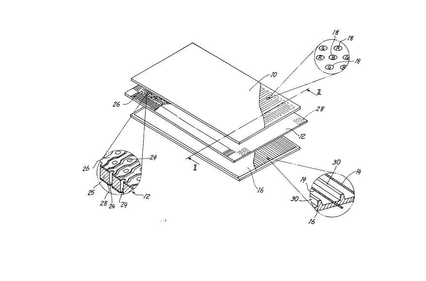
Fig. 1 is a perspective view showing a flat
display of the invention as exploded and also showing
main portions thereof on an enlarged scale;
Fig. lA is a plan view showing the position of
spacer ridges as related to an arrangement of phosphor dots;
Fig. 2 is an enlarged fragmentary view in
vertical section along the line II-II in Fig. 1 and
showing the flat display as assembled;
Fig. 3 is a plan view showing the inner surface
of a rear panel;
Fig. 4 is an enlarged fragmentary perspective
view of the rear panel;
Fig. 5A and Fig. 5B are enlarged sectional views
--8--
,.. ~ , . ., . . ~ . .
.: - . ~ - .
.
t ' ' ' . ' ' ~ ~, ' ' ' :
' ' :,. ' ' ' . ' '' " "'` ` ' ' '
. ' ' ~ . .. .
' ' ' ~' " , -, ' ~
.,
, ' ' ' ' " . , ` ' . . ~:
200~292
showing an electron beam as projected on a front panel
when the spacer ridge has slanting side faces;
Fig. 6A and Fig. 6B are enlarged sectional views
showing an electron beam as projected on the front panel
when the spaer ridge has vertical side faces;
Fig. 7 is a perspective view partly broken away
and showing a flat display having a spacer panel;
Fig. 8 is an enlarged fragmentary view in
vertical section showing a flat display having a spacer
panel with apertures of the same diameter as those in an
address electrode plate;
Fig. 9 is an enlarged fragmentary view in
vertical section showing a flat display having a spacer
panel with apertures of a smaller diameter than those in -
the address electrode plate;
Figs. lOA, 10~ and lOC are diagrams showing the
position relationship between an aperture and two
address electrodes;
Fig. 11 is a diagram of an arrangement of
circular apertures;
Fig. 12 is a diagram of an arragement of
rectangular apertures;
Fig. 13 is a perspective view partly broken away
and showing a flat display having a spacer panel with
tapered aperturesi
.. ~ . . . .
- ,, ,.... ~.;.. ;, . .: .
2003292
Fig. 14 is a fragmentary view in vertical
section of the flat display of Fig. 13;
Fig. 15 is a plan view showing the flat display
of Fig. 13 wherein the spacer panel apertures are
displaced to the greatest extent from the address
electrode plate; and
Fig. 16 is an exploded perspective view
partly broken away and showing a conventional flat display.
DETAILED DESCRIPTION OF EMBODIMENTS
Several preferred embodiments of the invention
will be described below in detail.
Fig. 1 shows a flat display embodying the
invention and serving as a color display. The display
comprises a front panel 10, a rear panel 16 and an
address electrode plate 12 disposed between the two
panels.
The front panel 10 is a large panel measuring
880 mm in horizontal length, 497 mm in vertical length
and 3 to 4 mm in thickness and is formed with phosphor
dots 18 of the three primary colors, red, blue and green,
as arranged regularly at a specified pitch over the
entire inner surface (see Fig. lA) . The inner surface
of the front panel and the areas between the phosphor
dots 18 are coated with carbon to ensure an improved
contrast. The carbon coating and the dots are coated
--10--
, . . : .: .. ~ .: : -
.. . . . -
. . . . . . .. .
. .; ~ . . -
.
~ ,~ ' "`-' ' ' `
. . . . .
with a thin metal back layer 22 of aluminum as seen in
Fig. 2 to prevent-charqing.
The rear panel 16 is made of a glass plate
3 to 4 mm in thickness and joined at its periphery to
the inner surface of the front panel 10 to form a
display panel unit.
Linear filament cathodes 14 held at their
opposite ends by anchors 15, 15 (see Fig. 3) extend as
tensioned over the inner side of the rear panel 16.
The cathode 14 is in the form of a tungsten wire having
a diameter of 30 to 50 micrometers and coated with an
electron emitter material such as barium oxide and is
held away from the rear panel 16 by the anchors 15 as
shown in Fig. 2. As shown in Fig. lA, the cathodes 14,
345 in number over the entire panel 16, are arranged
in parallel at a spacing of every three horizontal
(lateral in the illustration) rows of phosphor dots 18.
With reference to Figs. 1 to 4, spacer ridges
30 having a height of about 0.3 mm to reach the address
electrode plate 12 are formed on the inner surface
of the rear panel and arranged between the respective
filament cathodes 14. The spacer ridge 30 is tapered
toward the address electrode substrate 12 and has opposite
side faces which are inclined toward each other at the
same angle with the surface of the rear panel 16.
--11--
-- . . . .
: . , '', , ~ . - '
:: - . ., ..... ,.,, . :.. . -
. -
.
,
~:.
. . . . ~
Z00329Z
As shown in Fig. 2, the inner surface of the
rear panel 16 and the side faces of the entire lengths
of spacer ridges 30 are covered with a metal film to
form a back electrode 32.
An alternating current of 100 kHz with a
central voltage of zero V and an amplitude of i2 V
is passed through the cathodes 14 to release free '
electrons, while the back electrode 32 is maintained at
d.c. zero V or a slightly higher potential, facilitating
release of electrons from the peripheries of thecathodes 14.
The address electrode plate 12 comprises a
substrate 25 having a thickness of 1 mm and made of glass
or a ceramic, first address electrodes 26 formed on
ona of the surfaces of the substrate 25 along the Y-
direction (vertical direction) of an XY matrix and
corresponding to the respective rows of phosphor dots
18 present in,the same direction, and second address
electrodes 28 formed on the other surface of the substrate
25 directed in the X-direction (horizontal direction) of
the XY matrix, i.e. in a direction perpendicular to the
first address electrodes 26, and corrsponding to the rows
of phosphor dots present in the same direction. The
first address electrodes 26 are arranqed in parallel and
3143 in number in corresponding relation to the number
-12-
'." ~ .'' . ', . . -
::: . . ,
. ' ' " ' ~ , . '. ` '
: ' ~ ' :' .
of phosphor dots arranged in the horizontal direction
on the front panel 10. An address signal voltage in
the horizontal scanning direction is applied to these
electrodes in succession. On the other hand, the second
address electrodes 28 are arranged in parallel and 1035
in number in corresponding relation to the number of
phosphor dots arranged in the vertical direction. An
address signal voltage in the vertical scanning direction
is applied to these electrodes in seccession.
The intersections of the two electrodes 26, 28
correspond to the respective phosphor dots 18 in
position. Apertures 24, 24a, 24b, extending through the
electrodes and the substrate, are formed in the address
electrode plate 12 at the positions of the intersections
over the entire area of the plate as shown in Fig. 2.
The address electrode plate 12 is supported
by the upper ends of the spacer ridges 30 at positions
where the apertures 24, 24a, 24b are not closed therewith,
and is adhered to the ridges when required for preventing
2~ warping and vibration. The electrode plate 12 is
supported at a level of 0.3 mm from the inner surface of
the rear panel 16.
Further as seen in Figs. 3 and 4, the adjacent
spacer ridges 30 are interconnected by short auxiliary
spacers 34 at several locations along the length thereof.
-13-
, , -:. :. .,. ,: -
,.: :
200329Z
The filament cathode 14 is fitted in a recess 35 formed
in the top of the auxiliary spacer 34 at the midportion
thereof and is prevented from contacting the second
address electrode 28 when loosened or vibrated upward
and downward. Since the cathode 14 is in point-to-point
contact with the auxiliary spacer 34 at the recess 35,
the cathode 14 undergoes almost any temperature drop
due to heat transfer despite the contact and therefore
releases electrons free of trouble.
Between the two spacer ridges 30, 30, three
apertures 24, 24a, 24b are formed symmetrically with
respect to the cathode 14, with the central aperture
24 positioned immediately above the cathode 14 as ~`
shown in Fig. 2, so that when the phosphor dot 18
immediately above the central aperture 24 is addressed,
electrons can be released easily toward the addressed
dot 18. Electrons also flow smoothly toward the phosphor
dots at the opposite sides as will be described below
since electxon beams 40 temporarily extend sidewise and
are then deflected toward the apertures 24a, 24b by being
drawing by the electrodes 26, 28.
Figs. SA and 5B show electron orbits determined
by computer simulation. Fig. 5A shows a case wherein
a phosphor dot immediately above the cathode is
addressed, and Fig. SB a case wherein a phosphor dot
.. . . . .
' .~ ' '' '
" .
.. . .
.. . ,,
2003292
at one side of the cathode is addressed.
In the case of Fig. 5B, an electron beam 40
flows sidewise free of trouble and impinges on the dot
18 in alignment with the aperture 24a. ~e have found
that the area over which the fluorescent screen is
irradiated with the electron beam 40 above the aperture
is not different substantially between the case wherein
the electron beam passes through the aperture immediately
above the cathode as seen in Fig. 5A and the case where
l0 the beam passes through the side aperture 24a or 24b as -
shown in Fig. 5B. Thus, the beam impinges on the
picture element reliably to form a bright sharp image.
On the other hand, the result of simulation ~;
made in the case where the spacer ridge 30 has vertical
side faces as seen in Fig. 6A and Fig. 6B indicates
that the area of irradiation of the fluorescent screen -~
differs with the position of the aperture for passing
the electron beam 40 therethrough. This difference, if
grea., produces irregularities in the luminance of
images.
The difference between the electron orbits
appears attributable to the difference in the potential
distribution in the portion defined by the spacer ridges
30, the rear panel 16 and the address electrode plate 12
between the slanting side faces of the spacer ridges 30
-15-
.. ~ . ~ :,, ,: . - : .
- . , . - : : - . :.. :
. . . . ~ : . , ~: . ,:
. ~ : . .: . :: . .. ,:... -
. :. . : . ..
: . : . . . ~
:. . , - - ~ ~
shown in Figs. 5A and SB and the vertical side faces of
the ridges 30 in Figs. 6A and 6B. It is thought that
owing to the difference in the potential distribution,
the orbit of electrons released from the filament cathode
S 14 so changes as to produce almost no change in the area
of impingement of the electron beam on the front panel
10 regardless of whether the beam passes through the
central aperture or the side aperture in the case of
Figs. 5A and 5B.
Fig. 7 shows another embodiment of the inven-
tion wherein the rear panel 16 is formed with spacer
ridges 30, and a spacer panel 36 about 1 mm in thickness
and made of glass, ceramic or like insulating material
is disposed in the space between the front panel 10 and
the address electrode plate 12. The spacer panel 36
has over the entire area thereof apertures 38 positioned
in alignment with the respective apertures 24 of the
electrode plate 12. Accordingly, the electron beam
freely passes through the two apertures 24, 38 to impinge
on the phosphor dot 18.
With the flat display of Fig. 7, the spacer
ridges 30, the address electrode plate 12 and the spacer
panel 36 are provided between the front panel 10 and
the rear panel 16 to support the panels 10 and 16 and
give remarkably improved pressure resistance to these
-16-
. . . .
. . ,
: ` ' ` ' ' : ~` .: '.
. . .:
- . - : - - - - : :
.
Z003292
panels.
Fig. 8 shows another embodiment of flat
display comprising spacer ridges 30 and a spacer panel
36. The spacer panel 36 has apertures 38 having the
same diameter as the apertures 24 of the address
electrode plate 12.
Fig. 9 shows another embodiment which is an
improvement of the embodiment of Fig. 8 in that the
apertures 38 formed in the spacer panel 36 have a smaller
diameter than the apertures 24 in the address electrode
plate 12 and that the address electrodes 26 of XY
matrix to positioned closer to the front panel are
formed on the lower surface of the spacer panel 36.
With the embodiment of Fig. 9, the address
electrodes 26 are exposed to the interior of the
apertures 24 of the electrode plate 12 over an increased
area, so that the electron beam can be drawn easily.
The voltage to be applied to the address electrodes 26
can thexefore be lowered to achieve a reduction in
power consumption.
When the fluorescent screen luminesces
monochromatically, the apertures 24, 38 to be formed in
the address electrode plate 12 and the spacer panel 36,
respectively, are identical with the picture elements
on the screen in size and pitch. In this case, the
. , , -.. ... . . .... .. . . . . . ... .
,
., .... , . ....... , , ............ . -:
. . ' ' :
spacer ridges 30 to be formed on the inner surface of the
rear panel 16 are arranged at a spacing of one pitch or
a plurality of pitches of the picture elements.
With the above embodiment, the intersection
S of the first address electrode 26 and the second
address electrode 28 on opposite sides of the substrate
25 of the electrode plate 12 is formed with one aperture
24 centrally of the inLersection as shown in Fig. 10A.
Owing to an accumulation of errors in making the apertures
and the electrodes of the embodiment, it is likely that
the aperture 24 is positioned away from the center of
the intersection of the electrodes 26, 28 as seen in
Fig. 10 . In an extreme case, as in Fig. 10C, the aperture 24 is
formed completely outside the electrode intersection. This
lS means that the corresponding picture element totally
fails to luminesce to produce images of impaired quality.
~ his problem can be overcome by forming a
multiplicity of apertures 24 in the substrate 25 of the
electrode plate 12 in a close arrangement without any
lapping of the adjacent apertures with at least one
aperture formed in each of the intersections of the
electrodes 26, 28.
For example in the case where the apertures
24 are circular in cross section, suppose the diameter
of the apertures 24 is Da, the shortest distance
-18-
~ . , .~.. , , - :. .
. ~ . : ~ , :, ,. - -.
. . - . . . .
: - . , - :
:, : .. ---
. ~:
2003292
between the adjacent apertures is Ia, the width of the
second address electrode 28 is Wxg, the clearance
between the electrodes 28, 28 is Ixg, the pitch of the
second address electrodes is Pxg, the width of the
first address electrode 26 is Wyg, the clearance between
the electrodes 26, 26 is Iyg, and the pitch of the first
address electrodes is Pyg as shown in Fig. 11. These
dimensions are to be determined as follows.
Wxg = k x (Da + Ia)
Ixg = 1 x ~Da + Ia)
Pxg = (k + 1) x (Da + Ia)
Wyg = m x (Da + Ia)
Iyg = n x (Da + Ia)
Pyg = (m + n) x (Da + Ia)
wherein k, 1, m and n are each an integer.
Thus, the width and pitch of and the clearance
between the first electrodes 26, as well as the second
electrodes 28, are each so determined as to be equal
to the sum of the diameter of the aperture 24 and the
shortest distance between the adjacent apertures 24,
i.e. (Da + Ia), multiplied by an integer. In the case
of Fig. 11, k = 3, 1 = 1, m = 4 and n = 1.
Fig. 12 shows an embodiment wherein the
apertures 24 are rectangular in cross section. Suppose
the width of the aperture 24 in the direction of the
--19--
: . ~ -. - - . - . .
. .
200:~29Z
first address electrode 26 is Wax, the width thereof
along the second address electrode 28 is Way, the
distance between the apertures which are adjacent to
each other in the direction of the address electrode
26 is Iax, the distance between the apertures adjacent
to each other in the direction of the second address
electrode 28 is Iay, the width of the second address
electrode 28 is Wxg, the clearance between the electrodes
28 is Ixg, the pitch thereof Pxg, the width of the first
address electrode 26 is Wyg, the clearance between the
electrodes 26 is Iyg, and the pitch thereof is Pyg.
These dimensions are to be determined as follows.
Wxg = k x ~Wax + Iax)
Ixg = 1 x (Wax + Iax)
lS Pxg = (k + 1) x (Wax + Iax)
Wyg = m x (Way + lay)
Iyg = n x (Way + lay)
Pyg = (m + n) x (Way + Iax)
wherein K, 1, m and n are each an integer.
Thus, the width Wxg of the second address
electrode 28, the distance Ixg between the electrodes
28, 28 and the pitch Pxg thereof are each so determined
as to be equal to the sum of the width Wax of the
aperture 24 in the direction of the address electrode
26 and the clearance Iax beween the apertures adjacent
-20-
.. . . .
.. ,~ ,. ... ..... . . - ~- : - : .
.
200329:~
along the first address electrode 26, i.e. (Wax + lax),
multiplied by an integer. The width Wyag of the first
address electrode 26, the clearance Iyg between the
electrodes 26 and the pitch Pyg thereof are each so
determined as to be equal to the sum of the width Way
of the aperture 24 in the direction of the second address
electrode 28 and the clearance Iay between the apertures
adjacent along the second address electrode 28, i.e.
(Way + Iay), times an integer. In the case of Fig. 12,
k = 3, 1 = 1, m = 4 and n = 1.
Figs. 13 and 14 show a flat display wherein
a multiplicity of apertures 42 are formed in the address
electrode plate 12 at a small pitch so that at least one
aperture is present at each of the in~ersections of the
electrodes 26, 28. In .he illustrated case, 12 apertures
42 are formed in ~he area of each intersection.
With this flat display, the spacer panel 36
is formed with apertures 44 at the same pitch as the
pitch of phosphor dots on the front panel 10. The
apertures 44 are tapered from one side of the panel 36
close to the electrode plate 12 toward the other side
thereof close to the front panel 10, with a cross
section diminishing in this direction. At the electrode
plate side, the apertures 44 have the largest possible
area without overlapping, and the opening area is
-21-
.. ' , ' '- '.. ' : ~ . .,:,
' . ., . ' ' - :
,.: ,
.
2003Z92
sufficiently greater than the aperture 42 in the
address electrode plate 12.
Accordinqly, even if the aperture 44 of the
spacer panel 36 is displaced from the corresponding
S aperture 42 of the electrode plate 12, electrons are
assured of a sufficiently large region to pass through.
For example, even in the worst case where the
two apertures 42, 44 are displaced to the greatest
extent as shown in Fig. 15, the hatched areas for
electrons to pass through straight are sufficiently
large to excite the phosphor dot.
When an address signal voltage is applied to
the address electrodes 26, 28 of the electrode plate 12
in the above flat display, electrons are drawn from the
filament cathode 14 most proximate to the addressed
position, dividedly passed through a plurality of
apertures 42 at the addressed position of the electrode
plate 12, then guided through the aperture 44 in the
spacer panel 36 and efficiently irradiate the phosphor
at the corresponding position on the front panel 10.
Accordingly, the flat display of Fig. 13 not
only has improved strength against pressure due to the
provision of the spacer ridges 30 and the spacer panel
36 but also affords sharp images without irregularities
in luminescence.
-22-
. ..
. : . .. . -: ,: . :
- -. - ~ . . :
., ,. ~ - . ; : ' ' - ' ' ~, ' '
;, ., . ' ' ' . '~ . .' ~ .''''
~ . - . ~ -
." " : . - : -
~0032~2
The drawings and the foregoing description
of the embodiments are intended to illustrate the
present inven~ion and should not be interpreted as
limiting the claimed invention or reducing the scope
S of the invention.
The construction of the displays of the -
invention is not limited to the foregoing embodiments
but can of course be modified variously by one skilled
in the art without departing from the scope of the
invention as defined in the appended claims-;
-23-
~ .
,.. , . ~. . ... . , . . .......... ~ . . ..
.. . ,: - ~ : , . -