Note: Descriptions are shown in the official language in which they were submitted.
X003S79
DIRECTIONAL WAVEGUIDE-FINLI~E COUPLER
'
BACKGROUN~ OF THE INV~NTION
This invention relates to cylindrical waveguides. More
specifically, this invention is a waveguide coupler used to couple a
portion of the energy propagated through one waveguide into another
waveguide. ~-
It i8 frequently necessary to sample the signal being
transmitted through a waveguide, for example, to measure standing
wave ratios or output power from a transmitter. Prior art waveg~ide
couplers coupled radio frequency energy in one waveguide into an
adjacent waveguide by physically placing two rectangular waveguides
together BO that the walls of the two waveguides in contact form a
common wall through which slots or apertures are cut at
predetermined intervals to permit electromagnetic energy in one
waveguide to radiate into the other waveguide. The slots or apertures
cut in the common wall of the two waveg~udes generally have
predetermined geometries that permit energy transfer from a first
waveguide into a second waveguide such that directional wave
propagation will occur in the second waveguide. These spaced
apertures or openings require close matching tolerance~ and precise
spacing to accomplish an efficient energy transfer from one
waveguide to the next. :
Frequency dependency constitutes another problem with prior
art couplers. Apertures of any given size and spacing permit more
coupling at higher frequencies than they do at lower frequencies.
When employed in broadband applications, a coupler, using spaced
apertures, will couple different frequencies, at different levels.
Spaced apertures might also exhibit two-directional signal
propagation in the coupled waveg~ude, when the ~lots or apertures
are not spaced V4 of their wavelength of the coupled signal (i.e., ~ i
signals in the coupled waveguide might propagate in both
directions).. Thi~ bi~directional coupling occurs when wavefronts in
35 the coupled waveguide do not properly add in the desired direction
and the wavefronts in the coupled waveguide do not properly cancel in
the opposite direction, all because of inexact slot spacing.
~ '`,..';'.'':" ,
. :," ~
, ~',
2G035~9
When one waveguide is used across a relat*ely wide range of
frequencies, the level of coupling might change substantially from one
end of the frequency range to another when using only a single set of
apertures for the coupler. When using spaced aperture couplers with
5 a waveguide that carries signals across a relatively wide frequency
range, it is frequently necessary to cascade many pairs of coupling
apertures, each optimized for small segments of the frequency range.
An alternative i8 to cascade separate frequency couplers, with each
coupler being optimized for frequency band. Of course a disadvantage
10 of having to cascade several spaced aperture couplers in a waveguide
system is the added cost, weight and complexity of the transmission
line. A waveguide coupler which is inherently less frequency
dependent and easier to fabricate would be an improvement over the
prior art.
SUMMAR~ OF T~IE INVENl~ION
The present invention provides a waveguide coupler that does
not use spaced apertures cut between adjacent waveg ude walls
thereby eliminating the associated frequency-dependent transfer
20 characteristics and precision machining requirements of prior art
couplers. This waveguide coupler nevertheless provides a
substantially flat frequency response across a relatively wide range of
operating frequencies.
In one embodiment, the invention provides a waveguide coupler
25 for coupling a portion of a signal in one waveguide, hereafter referred
to as the source waveguide, into an adjacent waveg~ude, hereafter
referred to as the coupled waveguide, both waveg~udes sharing a
common wall. The coupler is comprised of a waveguide-mode-to-
finline-mode con~rerter that converts TE or TM waves or waveguide
30 mode propagation signals to fin-lin-mode waves. After energy in the
source waveg~ude is converted to fin line mode, a portion of the energy
iB transferred from the source waveguide to a coupled waveglude
through a single aperture, which is a slot cut through the common
wall separating the two waveguides and orthogonal to the cross-
35 section of the two waveguides. A fin line pair is located in theaperture and is the mechanism by which energy in the source
waveguide i8 transferred to the coupled waveguide.
. : :
ZGO~S~9
Energy propagating in the source waveguide is transferred
across the aperture in fin line mode. The transferred energy in the
coupled waveguide in the fin line mode may be reconverted from fin - -
line mode to waveguide mode whereupon the propagation of
6 electromagnetic energy through the wave guide continue~ in
waveguide mode. Electromagnetic energy in the source waveguide
after being converted into fin line mode and after traversing the fin
line coupling mechani~m in the common waveguide wall may also be
converted back to waveguude mode from fin line mode whereupon
10 microwave energy continues to propagate through the waveguide
normally. The coupler i8 directional in that energy in the coupled
waveguide propagate~ in only a single preferred direction.
The degree of tightness of coupling from the source waveguide
to the coupled waveguide is controlled by the dimensions of the fin line
15 mode coupler, the physical dimensions of the slot in the waveg~ude
wall, and the length of the coupler in the waveguide. Coupling
coefficients can be empirically determined to fix the desired ratio of
input power to coupled power for any particular waveguide and
geometry.
ao " .,. "
BRIEF DESCRIpTION OF TH~ 12~1NGS
Figure 1 shows a microwave transmission system including a
transmitter, waveguude coupler, and antenna.
Figure 2 shows an isometric cross-sectional view of the
25 waveguide coupler.
Figure 3 shows representative electric field lines in the
waveg~ude coupler of Figure 2.
Figure 4 shows an isometric, cross-sectional view of the
invention with the fin line mode coupler including smooth shaped
30 mode converter transition regions.
Figure 6 shows a top view of the fin line mode coupler used in
the invention including mode converter sections on each end.
Figure 6 shows a graph of the frequency dependency of the
output of the coupler of the preferred embodiment from 17 gigahertz to
24 gigahertz. ;~
~ .
ZG~3579
Referring to figure 1 there is shown a simplified microwave
transmission system 5. A microwave transmitter 15 deliver3
microwave energy through waveguide 20 to an antenna 30. A meter
25 shows what power levels are delivered through waveguide 20 to
5 antenna 30.
Meter 25 measure~ the level of power propagating in waveguide
20 by means of coupler 10, which couples a percentage of the power
propagating through waveguide 20 into waveguide 21. The energy
coupled into waveguide 21 propagates to power meter 25. By means of
10 coupler 10, a small, predetermined percentage of power propagating
through waveguide 20 is diverted into waveguide 21 and to power
meter 25 such that power meter 25 can be calibrated to reflect actual
conditions in waveguide 20 by scaling the readings of meter 25.
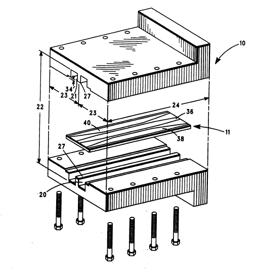
Referring now to figure 2, there is shown an isometric cross-
sectional view of coupler 10 shown in Figure 1. Coupler 10 i8 ~ `
comprised of two adjacent parallel waveguide sections 20 and 21, each
having a predetermined length 24 and each having a wide dimension
22 that is at least equal to one-half the wave length of the lowest
frequency signal propagating in the waveguide 20. Those skilled in
20 the art will recognize that wide dimension 22 must be at least equal to
one-half the longest wavelength propagated through waveguide 20 to
permit energy propagation through the waveguide.
Microwave energy propagating in waveguide 20 is coupled into
the adjacent waveguide 21 by means of a fin line ~tructure 11,
25 described below and shown in figure 6, inserted into waveguides 20
and 21 through the slot 34, cut through the waveguides common wall
27. In the preferred embodiment, slot 34 is cut through the common
wall 27, in a direction orthogonal to the cross-sections waveguides 20
and 21. (one-half of slot 34 shown in figure 3 is ~hown by the depth of
30 the chamber 34shown in figure 2). The width of 810t 34 is adjusted,
along with the length 24 of the coupler 10 and the spacing of
conductors of the finline structure 11, (as shown in Eigure 5) to
determine the degree of coupling between the two waveguides 20 and
21. -
With reference to Figure 5, a finline mode structure 11 is
inserted into the common wall section 27 of coupler 10. Fin line mode
structure 11 is comprised of conductors 36, 38 and 40 on a non-
metallic substrate 41. The portions T1, T2, and T3 of fin line mode
., , . -- .
X0~13579
structure 11, of conductors 36, 38 and 40, comprise a fin line mode
converter 13, which transform the wave propagating through
waveguide 20 ~rom waveguide mode to fin line mode. Electromagnetic
fin-line-mode waves propagating through coupler 10 produce electric
5 fields across conductors 38 and 36 which in combination with the slot
34 located in common wall 27 of waveguide 20 and 21, effects the
transfer of energy from waveguide 20 into 21. Energy transfer iB :
accomplished by means of the electric field set up along the length of
the common fin line conductor 36 across the common wall aperture.
Referring now to Figure 3, there is shown a cros~ sectional
diagram of the electric field that would exist in coupler 10 as shown in
figures 1 and 2. Electromagnetic energy propagating in waveguide 20
is first converted from waveguide mode to fin line mode along the
transition regions T1, T2 and T3 of conductors 36, 38 and 40 to produce
1~ the electric field lines E1, E2 and E3 of Figure 3. Electric field line~
are shown originating from conductor 38 and terminating at center
conductor 36 in waveguide 20. However, the reverse polarity may
equally represent the field pattern. The slot 34 cut through the
common wall 27 of waveguide 20 and 21 permits the development of
2û electric field line~ E3 and E6 from h common wall 27 across slot 34 to
the center conductor 36 as shown. The termination of flux acro~s the
slot 34 to conductor 36 establishes an electric field distribution in
waveguide 21 that is similar to the electric field distribution as shown
in Figure 3. Electric field lines E4 and E5 in waveguide 21 are shown
originating from conductor 40 and terminating on the center
conductor 36. Electric field lines E6 originate at center wall 27 and
terminate at center conductor 36 of the fin line mode structure 11.
The reverse polarity may equally represent the field pattern. The
development of the electric field in waveguide 21 is accomplished by
means of the fin line coupling mechanism located in slot 34 in the
common wall 27. The transfer of fin line mode microwave energy
through the slot 34 establishes electric fields in waveguide 21. In the
absence of the fin line coupling mechanism, no energy transfers
through the slot 34 in the common wall 27.
Note that when energy is transferred into waveguide 21 acros~
the slot 34, the energy transferred into waveg~ude 21 propagates in the
same direction as the direction of propagation in waveguide 20. There
is little energy propagated in the opposite direction as is seen with
6 2Go3 5~9
multi-aperture couplers because coupling i~ accomplished by
common field effects rather than aperture radiation.
The strength of the electric fields and correspondingly the
amount of coupling, (i.e., the amount of power delivered into
5 waveguide 21 from waveguide 20), i8 dependent upon the spacing of
conductors 36,38 and 40, the width of the slot 34 and the overall length
24 of the fin line coupler 10. Tho~e skilled in the art will recognize
that as the spacing between conductors 36,38 and 40 becomes smaller
the density of the electric field lines will increase accordingly.
10 Increased density of the fields about the gap between conductors 36,
389 and 40 permits more power to be transferred through the slot 34,.. --
Conversely, increasing the width of the slot 34 in the common wall 27
increases the coupling by permitting an increased portion of the total
field to span slot 34. Also, asymmetrically locating the gaps between
15 conductors 36,38 and 40, closer to the common wall 27, increases the
coupling level.
Referring to figure 4 there is shown another isometric cross-
sectional view of the coupler 10 of the present invention. The
conductors 36,38 and 40 are shown with transition regions T1, T2 and
20 T3 which in the preferred embodiment are cosine2 tapers of metal
sections deposited onto a dielectric substrate. The transition regions
T1/T2 and T2/T3 respectively perform the waveguide mode to fin line
mode conversion enabling the coupling to take place along the fin line
coupler which is formed by the remainder of conductors 36,28 and 40,
25 beyond the tapered transition region. Similar wave shapes for the
transition regions might include sin e squared, linear logarithmic or
other mathematical functions. In the preferred embodiment, the
thickness (t as shown in figure 3) of the dielectric upon which the fin
line mode coupler was deposited is selected 80 as to hold electrical
30 conductor 36 in contact with common wall 27.
Referring again to figure 5, there is shown a top view of the Sn
line mode structure 11 of the invention. Transition regions T1, T2 and
T3, included at both ends of conductors 36, 38 and 40, are shown that
accomplish the waveguide mode to fin line mode conversion along a
35 predetermined length of the coupler and also include a similar set of
transition regions T1, T2 and T3 to perform a fin line mode to
waveguide mode conversion, enabling propagation through the
waveguide to continue normally as it had in the waveguide ahead of
' . ~ ': ..
" :''''~
.' '" ~:
2003s79 -
the coupler 10. Conductor~ 36, 38 and 40 cannot merely be suspended
ill the waveguide 20 and 21 as ~hown in figures 1, 2, and 3 for
illus~a~ve purpo~e~ but mu~t be held fi~ed relati~e to the aperture.
Conductors 36, 38 and 40 are deposited onto a dielectric material such
5 as DuroidTM or alO and positioned appropriately in the two adjacent
waveguides 20 and 21 as shown in figures 1, 2 and 3. In the prefemd
embodunent electrodes 36, 38 and 40 are teposited on DuroidTM,
manufactured by the Rogers corporation, the thickness of which
when inserted into the waveguide 20 and 21 holds conductor 36 in
10 electrical contact with the waveguide common wall 27 and maintain~
the slot 34 as shown in figure 3.
I~ the prefelTed embodunent a directional fin line coupler i8 :.
used in a wa~reguide operated from 17 gigahertz to 24 gigahertz. Test
results of the energy coupled by the waveguide coupler of the invention
15 a showD in Figure 6 ~how that across this 7b ~igahertz frequency
range the amount of coupling from waveguide 20, to wareguide 21
changed less than 2 decibels. The coupling form waveguide 20 to
waveguide 2rat 17 g~ahertz was appro~imately - 16 dB, while at 24
gigahertz the coupling remained at essentially - 16 dB dropping to
appro~imately -17 dB somewhere between 17 and 24 gigahertz as
shown.
'' "~
~ A
.. . ~..
. ..