Note: Descriptions are shown in the official language in which they were submitted.
7rj
COMPOSITE INCLUDING AN INORGANIC IMAGE ~ND
METHOD OF TRANSFE~RIN~ SUCH AN IMAGE
_
Technical Field
Broadly, the present invention relates to inor-
ganic film imaging and methods of transferring such an
inorganic pattern or image to a substrate. More specifical-
ly, the present invention relates to metal film imaging an~
methods of transferring such a metal pattern or image to a
substrate.
Background of the In~enkion
A wide variety of thin metal film patterns ar0
known and used in a variety of different applications.
Metal films are often used for either their decorative and
aesthetic characteristics, including specular reflectance,
or their ability to conduct electricity. Examples of decor-
ative uses include the use of metallic patterns upon wall-
paper, greeting cards, labels, business cards, book covers,
name plates, automobiles, bicycles, and the like. An
example of the use of thin metal film images for their
electrical conductivity is printed circuit boards. Detailed
patterns of electrically conductive metal films are used to
make flexible printed circuits used in computer applica-
tions and the like. Patterns used for such flexible conduc-
tive circuits are often extremely detailed with up to 100
individual and separate lines of metal per cm.
Metallic patterns can also be used to control
static electricity and protect against electromagnetic
radiation while permitting substantial portions of visible
light to pass therethrough. This allows the pattern to
protect an article surrounded thereby from electromagnetic
radiation and static electricity whilP permitting viewing
of the article through the pattern.
~or many of these end uses, it is desirable to be
able to transfer the metal image or pattern from a carrier
substrate or the like to its ultimate position upon a
substrate. For example, it may be desirable to transfer a
pattern onto an automobile tail ligh-t ox onto a greeting
card by simply pressing a carrier subs-txate containing the
image onto the tail light or greeting card and then remov-
ing the carrier substrate. Likewise, it may be clesirable to
transfer such a metal image to a package to protect the
contents of the package from static electricity.
Accordingl~, there is a need for a quick and
simple method of transfexring a metal pattern or image,
preferably of fins detail, to a transfer substrate. Like-
wise, a need also exists for a metal image or patterntransfer sheet or tape which can quickly and easily trans~
fer a metal pattern or image from the tape or sheet to a
transfer substrate.
There is also a need for a conductive metal film
substrate composite that has an embossed surface and con-
- tains metal film only within the recessed, grooves of the
embossed surface. Such a composite can be used to make
containers that can protect a component from static elec-
tricity without crayoning. Crayon, as used herein, refers
to the undesired transfer of conductive material to an
electronic component, such as ~rom the above-referenced
container to a component stored therein.
A need also exists for a method of forming a
pat~ern of multilayered inorganic films on a substrate that
does not involve etching and can be carried out at high
production rates.
Summary oi the Invention
The present invention provides a method of trans-
ferring an image to a transfer substrate compromising the
steps of: (a) providing an embossed substrate having a
relief surface that includes a raised surface portion and a
recessed surface portion; (b~ depositing an inorganic layer
onto said relief surface thereby providing an image layer
--3~
on the raised surface portion wherein a bond of strength X
is formed between the image layer and the raised surface
portion of the embossed substrate; (c) providing a layer of
adhesive on at least the image :Layer; (d) contacting the
layer of adhesive with a transfer substrate; (e) forming an
adhesive bond of strength Y between the transfer substrate
: and the image layer, wherein Y is greater than ~; and (f)
separating the embossed substrate and the transfer sub-
strate and thereb~ transferrin~ the image layer to the
transfer substrate. The embossed substrate is preferably a
flexible polymeric material. A.lternatively, th0 following
can be substituted for steps (a) and (b): an embossable
substrate is provided in unembossed form, the inorganic
layer is deposited upon a first surface of the substrate
and then the first surface of the unembossed substrate is
embossed to form the relief surface coated with an inor-
ganic layer.
The present invention also provides a method of
making an image transfer sheet or tape by the method set
forth above by simply replacing the transfer substrate with
- a release liner. The sheet or tape can then be used at a
remote location to transfer the image layer to a transfer
substrate by removing the release liner and contacting the
exposed surface of the image transfer tape or sheet to the
transfer substrate.
: The present invention also provides an inorganic
image/substrate composite comprising: (i) an embossed
substrate having a relief pattern formed therein, that
includes a raised surface portion and a recessed surface
portion, (ii) first and second inorganic layers adhered to
the raised surface portion and the recessed surface por-
tion, respectively, and preferably (iii) an adhesive layer
coated onto the first inorganic layer adhered to the raised
surface portion of the substrate.
The present invention also provides a method of
(h 7r~~
--4--
making a transparent and conductive composite comprising an
embossed substrate having a metal layer restrictad to the
recessed surface portion of the embossed substrate and an
article so made.
The present invention also provides a method of
making a pattern including inorganic layers comprisiny
multiple inorganic films and an article so made.
The present invention also provides a method of
making an image of a cond~ctive inorganic layer on a sub-
strate that is inexpensive to manufacture and has excellent
bonding of the metal to the substrate, and an article so
made.
As used herein ~image layer~' refers to an lnor-
ganic layer deposited onto the raised surface portion of an
embossed substrate. The ~image layer" is the image or
pattern that can be readily transferred from the embossed
substrate to a transfer substrate. The ~image layerl' may
consist of one or more inorganic films.
Brief Description of the Drawings
Fig. 1 is a schematic cross-section of an embossed
substrate useful in the present inven-tion.
Fig. 2 is a schematic cross-section of the em-
bossed substrate of Fig. l having an inorganic layer
deposited upon the embossed surface.
- 25 Fig. 3 is a schematic cross-section of the article
of Fig. 2 coated wi-th an adhesive layer over the raised
surface portions of the embossed surface.
Fig. 4 is a schematic cross-section of the article
of Fig. 3 having a transfer substrate laminated to the
adhesive layer.
Fig. S depicts the article of Fig. 4 wherein the
transfer substrate and the embossed substrate are being
separated.
33~
--5--
; Fig. 6 is a schematic cross-section of an alterna-
tive embodiment of the article of Fig. 4 wherein the ad~
hesive layer was coated onto the transfer substrate.
Fig. 7 depicts the article of Fig. 6 where the
transfer substrate and the embo,ssed substrate are being
separated.
Fig. 8 is a schematic cross-section of the em-
bossed substrate of Fig. 5 after separation of the embossed
and transfer substrates wherein a second inorganic layer
has been deposited into the reclessed surface portions of
the embossed substrate.
Fig. 9 is a schemAtic cross-section of the article
of Fig. 8 with a transfer substrate adhesively laminated
thereto.
Fig. lO depicts the article of Fig. 9 wherein the
transfer substrate and the embossed substrate are being
separated.
Fig. 11 is a schematic cross-section of an embos-
sable substrate having a powder layer over a first surface
thereof.
Fig. 12 is a schematic cross-section of the ar-
ticle of Fig. 11 after the embossable substrate has been
embossed to form a relief pattern upon th0 first surface
and loose powder has been removed.
Detailed Description of the Invention
Referring to Fig. 1, an embossed substrate lO is
shown having a relief surface 12 which includes raised
surface portions 14, recessed surface portions 16, and
sidewalls 18.
Referring to Fig. 2, an inorganic layer 20 is
shown which includes a first organic layer 22 coating the
raised surfaces 14 and a second organic layer 24 coating
the recessed surfaces 16.
Referring to Fig. 3, an adhesi~ve layer 30 is shown
which coats the ~irst inorganic layer 22 coating the raised
surfaces 14.
Referring now to Fig. 4, a transfer substrate 40
is shown in contact ~ith the ad:hesive layer 30. The ad~
hesive is selected so that the adhesive bond between trans-
fer substrate 40 and inorganic layer 22 is greater than the
strength of the bond between the raised surface portion 1
and inorganic layer 22. Such relative bonding strength
.10 ensures that when txansfer substrate 40 and embossed sub-
strate 10 are separated, inorganic layer 22 will cleanl~
separate from the raised surface portion 14 and remain
bonded to transfer substrate 40.
Referring now to Fig. 5, transfer substrate 40 is
shown being separated from embossed substrate 10. Inorganic
: layer 22 separates from embossed substrate 10, while
remaining bonded to transfer substrate ~0. Inorganic layer
24 coating recessed surfaces 16 remains bonded to embossed
substrate 10.
Referring now to Figs. 6 and 7, an alternative
embodiment of the present invention is shown. In this
embodiment, adhesive layer 30 is coated onto transfer
substrate 40 rather than onto the inorganic layer raised
surface portion 22 of embossed substrate 10. This will
result in the use of excess adhesive 30, but should not
affect the ability of the final article to achieve the
desired characteristics.
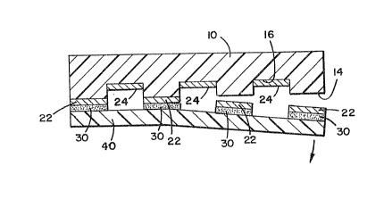
Referring to Fig. 8, the embossed substrate 10 of
Fig. 7 is shown after transfer substrate 40 has been
separated therefrom and removed inorganic layer 22 from the
raised surface portion 14 of the embossed substrate 10.
The inorganic layer 24 has been thickened by depositing a
second inorganic layer 82 over a first inorganic film 82
3~
coating the recessed surface portion layer 16 of embossed
substrate 10. The second inorganic layer 82 is deposited
within the recesses of the embossed substrate 10 such that
the second inorganic layer 82 is substantially flush with
the raised surface portion 14 of embossed substrate 10.
Referring to Fig. 9, an adhesi~e 50 coated trans-
fer substrate 40 is shown laminated to embossed surface 12
of embossed substrate 10. As in Fig. 4/ the adhesive 30 is
selected so that the adhesive bond between transfer sub-
strate 40 and second inorganic film 82 as well as the bondbetween second inorganic layer 82 and first inorganic film
80 are greatex than the strength of the bond between em-
bossed substrate 10 and the first inorganic film 80 of the
layer 24. Such relative bonding strength ensures that when
transfer substrate 40 and embossed substrate 10 are
separated, both first and second films 80 and 82 will
cleanly separate from embossed substrate 10 and remain
bonded to transfer substrate 40.
Referring now to Fig. 10, transfer substrate 40 is
shown being separated from embossed substrate 10. Due to
the relative bonding strengths discussed above, such sepa-
ration causes inorganic layer 24 to separate from embossed
substrate lQ and remain bonded to transfer substrate 40.
Referring to Fig. 11, an embossable substrate 110
is shown with a layer of inorganic powder 90 deposited on a
first surface 120 thereof.
Referring now to Fig. 12, the powder coated on an
embossable substrate 110 of Fig. 11 is shown after the
embossable substrate 110 has been embossed to form a relief
surface 12 to form raised surface portions 14 and recessed
surface portions 16. The powder layer 122 overlaying
recessed surface portions 16 has been pressure formed to
substantially evenly coat recessed surface portions 16 and
:
~ ~d3~
bond to the now embossed substrate 110 while the inorganic
powder 120 coating the raised surface portions 14 of the
now embossed substra-te 110 remains in a loose, powder form
and may be removed from now embossed substrate 110 by any
S of a number of means.
The present invention involves providing a relief
pattern upon a substrate 10 which is then coated with one
or more thin films to comprise inorganic la~ers 22, 2~.
The embossed substrate 10 can be made from any embossable
material having a sufficient st:ructural in-tegrity.
Preferred materials include plastics such as polypropylene,
polyethylene, polyesters, cellulose acetate, pol~vinyl-
chloride, and polyvinylidinsfluoride, as well as other
materials such as cellulose. One method of embossing the
substrate, is to extrude softened polymers onto a machined
embossing roll having an imprinted negative of the desired
pattern and then imprinting the design into the polymer.
Vapor coating is the prefexred method of deposit-
ing the inorganic films onto the embossed substrate 10.
Accordingly, the inorganic layers 22, 24 are preferably a
metal which can be vapor coated. The particular inorganic
material employed also depends upon the desired end use of
the resultant composite. For uses in which electrical
conductivity is important, metals which have a high elec-
trical conductivity should be chosen. When aesthetic char-
acteristics are important, materials with the desired
specular reflection, color, texture and the like should be
chosen.
It is preferred that the vapor coating be done at
an angle perpendicular to the relief surface 12 of the
embossed substrate 10 so that little or no inorganic is
deposited on the vertical walls 18 of the relief surface
12. Reducing the deposit of inorganic on the vertical walls
~ '7'~i
18 reduces the bond between the inorganic layer 22 on the
raised surface portions 14 and the inorganic layer 24 on
the recessed surface portions 1~ and thereby allows the
clean transfer of inorganic layer 22 to a transfer sub-
strate 40.
Suitable inorganics fo:r use as layers 22, 24
include aluminum, nickel, coppe:r, gold, silver, chromium,
indium, indium tin, indium tin oxide, alumina, silica, ZnS,
SiO, cryolite, titania, silicon, germanium, g~llium ar-
senide~ mixtures and alloys of these as well as mixtures of
the metals and alloys. In addition, multiple layers of the
same or different inorganic films may be applied, as
desired.
A wide variety of configurations may be selected
for the embossed substrate 10. The wide variety of end
uses of the present invention requires a wide variety of
different shapes~ sizes, configurations, patterns and the
like. In the decorative area, an enormous number of various
repeating and random shapes and sizes, such as squares,
circles, ellipses, he~agons, diamonds, triangles, dots,
etc., may be used. Also, this wide variety of different
shapes may be useful in the areas of static control and
electromagnetic radiation control. Printed circuits typi-
cally comprise a plurality of closely spaced lines inter-
~5 curved amongst each other in a pattern which provideselectrical conducti~ity between the desired positions on
the circuit board. Therefore, the pattern of such a metal
film would be dictated by its intended function. The image
or pattern which is desired for the end use is produced by
embossing the pattern into the embossed substrate 10. The
raised surface portion 14 of the embossed substrate 10
defines the ultimate pattern which will result and which is
capable of being transferred onto a transfer substrate. The
~r~ ~
--10--
present invention is capable of providing images or pat-
terns of fine detail. For example, 25-100 linear raised
surfaces 14 per cm or 625-10,000 raised surfaces 14 per
cm2, in the case of dots, squares, triangles and the like.
The thicknesses of the inorganic image or pattern
22 is typically determined by the desired end use and the
tolerances of the tooling used to emboss the embossed
substrate 10. For most end uses, when the inorganic layer
22, 24 are metal, a thickness of about 0.1 - 100 ~m is
useful. The depth of the recesses, i.e. the distance
between the recessed and raised surface portion, is typi-
cally about 10-1000 ~m.
A wide variety of adhesives may be chosen for use
as the adhesive layer 30 in the present invention. The
adhesive must be capable of forming a bond with inorganic
pattern or image 22 deposited on the raised surface portion
14 which is greater than the bond between the inorganic
pattern or image 22 and the embossed subs~rate 10. A wide
range of both thermoplastic and thermosetting adhesives are
useful. So long as the bond strength requirement is met,
pressure-sensitive adhesives such as silicones are par- -;
ticularly useful as the adhesive layer 30 in the present
invention.
~he adhesive layer 30, may be applied only to the
inorganic layer 22 on embossed substrate 10 by any of a
number of methods, including roll coating. Spray coated
adhesives may be applied to both raised 22 and recessed 24
inorganic surfaces. For some applications, ultraviolet
and/or electron beam curable adhesive resins may be desir-
able.
The inorganic substrate composites of the presentinvention may be provided in a number o~ useful forms, such
as sheets or rolls of transfer tape.
In an alternative embodiment, an inorganic layer
120 of a powder may be sprinkled onto an unembossed but
embossable substrate 110. By embossing the inorganic powder
120 coated surface of the embossable substrate 110 the
inorganic powder 120 within the recessed surface portions
16 will be mechanically bonded to substrate 110 while the
powder remaining on the raised sur-face portion 14 of the
substrate 110 will remain in loose powdered form and may be
easily removed from substrate 110.
Suitable inorganics available in powder form and
useful as layer 120 include metals such as aluminum, cop-
per, zinc, iron, nickel, cobalt and their alloys; ceramics,
such as alumina, titania, silica, tungsten carbide, boron
carbide, titanium carbide, and mixtures thereof.
The remaining composite of an embossed substrate
(10, 110~ having an i.norganic layer 120 on only the
recessed surface portions 16 may either be used as such or
may be further modified by depositing a second inorganic
layer 80 on-to inorganic layer 24 so as to fill the recessed
surface portions 16. rrhe second inorganic layer 80 may be
deposited onto embossed substrate 10, 110 by any suitable
means including dipping into molten inorganic which wets
only inorganic layer 24 or electroplatin~.
The multilayer pattern formed by inorganic layers
24 and 80 may be transferred to a transfer substrate 40 by
employing an adhesive layer 50 in accordance with the
earlier discussion.
By depositing additional inorganic layers or films
on the inorganic layer 24 provided on the recessed surface
portion 16 allows thicker layers of inorganic materials,
such as metall to be formed with the sidewalls serving as a
mold to insure that the layer is deposited uniformly with
sidewalls substantially perpendicular ~o the surface.
~ 3~ 7~i
-12-
Where additional layers of inorganic material are deposited
on free-standing layers, such as the metal stripes of a
conductive tape, variations in the width of the additional
layers can occur often causing closely adjoining stripes to
touch and make undesirable electrical connections.
The invention is furth~r described by the follow-
ing detailed examples.
~xample 1
A square piece of plexiglas 0.6 cm thick and 12.5
cm on a side had grooves cut into its ~urface with a
diamond saw. The grooves were 225 ~rn wide and 125 ~m deep.
The grooves were cut so as to leave the surface with rec-
tangular projections 75 ~m by 200 ~m for a density of about
800 rectangles per cm2. The grooved side of the plexiglas
was coated with about 0.15 um of aluminum in a vacuum bell
jar. A pressure sensitive acrylic adhesive tape (Scotch~
600 transparent tape DC/part no 021200-07457 available from
3M Co.) was laminated to the aluminum coated plexiglas.
Delamination of this tape transferred the metal deposited
on the top of the rectangular projections from the
plexiglas to the tape. The aluminum at the bottom of the
groves was not removed from the plexiglas.
Example 2
An embossed film of polypropylene was obtained
which had multiple square projections 50 ~m on a side. The
grooves separating the square projections were 50 ~m wide
and 50 ~m deep. This embossed film was vapor coated with
about 0.15 ~m of aluminum in a vacuum bell jar. The metal-
ized film was then laminated to a pressure sensitive ad-
hesive tape of the type used in Example 1. Subsequentdelamination of the tape transferred the 50 ~m by 50 ~m
squares of a]uminum from the polypropylene to the tape. Up
to at least 98 lines (dots) per cm or 9600 dots per cm2 can
-13-
be transferred by this process without a significant loss
in detail.
Exa~ple 3
A section of 250 ~m thick cast polyethylene terephtha-
late was embossed to provide a discontinuous major surface
of protruding squares 0.25 cm on a side. The squares were
separated from each other by recessed continuous surfaces
0.75 mm wide, and 0.125 mm deep which traversed the entire
len~th of the substrate and intersec-ted like surfaces so as
to form 90 degree angles therewith. This embo~sed film was
coated with copper by electron beam evaporation in a vacuum
roll coater to provi.de ahout a 0.15 ~m thick film of copper
over both the raised and recessed surfaces. The copper
coated raised surface was then laminated to pressure sensi-
tive adhesive tape of the type used in Example 1 using ahand held roller. Removal of the tape from the embossed
film removed the copper film from the raised surfaces which
permitted the passage of visible light through the raised
square surfaces. The copper in the recessed surfaces was
conductive and continuous.
~xample 4
The embossed substrate of E~ample 3, after removal
of the copper film from the raised surfaces, was placed in
a copper plating bath (copper sulphate bath) at room
temperature and electroplated at a current density of 0.006
amps per cm. Copper was plated until the thickness had been
increased to about 100 ~m.
~xample 5
The embossed substrate of Example 3, after removal
of the copper film from the raised surfaces was dipped into
a molten quaternary eutectic alloy of bismuth, lead, tin,
and indium at 86 C. Removal of the material from the
molten metal revealed that the metal had wet and coated
~ q~ r~ r~-
--14--
or~ly those regions containing copper, e g. the continuous,
recessed surfaces. Separation of the dip coated metal from
the polymer substrate provided for a self-supporting film
that reproduced the image of th~3 recessed surface of the
embossed film. The thickness of this metal film was about
200 ~m.
Exampl~ 6
The embossed film of Example 3 was coated with
alterllate layers of copper and llickel (0.15 ~m of copper,
0.15 ~m of nickel, 0.15 ~m of copper). This metal sand~lich
was spray coated with SCOTCH~ brand spray mount acrylic
adhesive, (available from the 3M Co. under cat. no. 6065
and ID No 62-6065-~826-1). The adhesive was bonded to
SCOTCHCAL~ brand release liner for further use. Later, the
release liner was removed and the imaged transfer tape was
laminated to KAPTON~, a polyamide available from DuPont,
and then delaminated to transfer the metal sandwich layer
to the polyamide. In like manor, such imaged metal layers
were also transferred to a variety of other substrates
including glass, paper and aluminum.
~x~mple 7
A 10 cm by 10 cm by 0.25 mm piece of cast poly-
ethylene terepthalate (PET) was coated on one side with a
layer of fine copper powder with an average particle size
of 50 ~m. The powder coating was just sufficient to com-
pletely cover the surface with a monolayer of particles. A
copper embossing plate, having a surface relief pattern
similar to that described in Example 3, was heated to 150 C
and pressed against the powder coated side of the PET for 5
seconds at a pressure of 70 kPa. A pattern of copper powder
corresponding to the pattern on the copper plate was em-
bedded into the surface of the PET. The excess copper
powder was brushed off the PET surface. The PET was then
3~
-15-
dipped into a solution of 1 part concentrated hydrochloric
acid and 9 parts water for 5 seconds, rinsed in water, and
dried. The PET was then dipped :Eor one second into a molten
quaternary eutectic alloy of bismuth, lead, tin, and indium
at B5 C. The molten metal wet the pattern of copper powder
embedded in the PET to form a square pattern of the bis-
muth-lead-tin indium metal on the PET. The resulting metal
pattern was roughly 50 ~m thick.