Note: Descriptions are shown in the official language in which they were submitted.
--~ 2003701.
MULTIPLE r~ANN~T. SERVO CONFIGURATION
BACKGROUND OF THE lNV~NllON
The present invention relates to digital servo
systems and, more particularly, to multiple channel servo
(MCS) systems utilizing an application specific integrated
circuit (ASIC).
It is known to use microprocessor controllers for the
real-time control of certain machine operations. To
illustrate, a mail processing system may be comprised of a
envelope feeder mechanism for receiving a stack of envelopes
and, in a serial manner, serving up the envelope to a
sealer-transport mechanism. The sealer-transport mechanism
is charged with the function of sealing each envelope as it
is caused to traverse a sealing apparatus and to serve-up
the envelope to a mailing machine. It is known to also
employ a scale mechanism located between the
sealer-transport mechanism and the mailing machine. The
scale mechanism is charged with the function of weighing the
envelope by means of a scale, and determining the required
postage value and communicating the postage value to a
postage meter. In similar manner, a transport mechanism,
customarily integral to the scale mechanism, must assume
physical control over the envelope for positioning the
envelope on the scale and thereafter serve-up the envelope
to the mailing machine.
Generally, the mailing machine will include a
transport mechanism which assumes control over the envelope
and deliver the envelope to a printing station whereupon a
postage meter will print a postage indicia on the envelope.
The mailing machine transport mechanism will again assume
control of the envelope and eject the envelope from the
mailing machine.
In the afore-described mail processing system,
envelopes are processed in a serial manner. In such mail
processing systems, it is known to provide each of the cited
mechanisms with a motor or plurality of motors to act as
prime movers for the associated mechanisms. As is known,
- 2 ~ ~ 3 7 1~ ~
each motor or group of motors is under the control of a
respective microprocessor motor controller acting through a
respective driver board. It is also known to provide the
respective driver board with a servo ASIC associated with
each motor or group of motor requiring servo control.
Such mail processing systems as afore-described have
required the use of multiple microprocessor motor
controllers and associated servo ASIC's.
- SUMMARY OF THE lNV~:N~'lON
It i8 an object of an aspect of the present
invention to present a MCS ASIC operable with a motor
controller system architected such that a single motor
controller can servo control a plurality of motors.
It i8 an ob;ect of an aspect of the present
invention to present a MCS ASIC operable under the direction
of a motor controller for servo-controlling a plurality of
motors wherein each of the controlled motors may be
individually servo-controlled, the control algorithm'for each
motor can be independently changed on the fly and the servo-
rate for each motor is independently selectable.
The MCS ASIC is a digital component designed to
provide high-performance servo control for dc motors. It
operates as a peripheral device under the control of a host
microprocessor which in the preferred environment is a
mailing system motor controller. The motor controller
performs digital filtering for closed-loop compensation.
The respective input channels of the MCS ASIC transforms the
signals from a respective motor position encoder into a
digital word through a quadrature decoder and up/down
counter, and the respective output channels transforms the
filter digital output into a pulse-width modulated (PWM)
signal.
There are eight (8) pairs of input/output channels
for supporting up to eight (8) servo loops, hence, eight (8)
totally-separate motor control channels. The necessary
digital logic and data processing for each of the servo
systems are performed onboard the MCS ASIC relieving the
- 3 - ~ 7 ~ ~
motor controller software of the time-intensive tasks of
digital control algorithm computations. Also the need for
additional hardware components for I/0 signal
transformations is eliminated.
To start the motor control process, the motor
controller is programmed to determine the motion profile for
each motor and provide to the ser~o loops of the MCS ASIC
with the desired motion commands which are discrete
positions for a time interval T. The servo loops are
initiated by a simply "start" command from the motor
controller to the MCS ASIC. The periodic rate "T" at which
the motor controller gives the position command to the
respective loops tells the MCS ASIC to start determining
the upper bandwidth limit of an individual servo control
channel.
At any time before receiving the first start command,
the MCS ASIC will allow the motor controller to download a
sequence of coded-data that configures the respective servo
channels to be enabled and configures the individual loop's
control algorithm. In general, when not executing the motor
control process, the MCS ASIC allows the motor controller to
access its internal memory map through a data bus. As a
result, for any servo channel enabled, the motor controller
can download (or alter) and examine the filter algorithm
coefficients, the filter output, the motor PWM command, and
the motor position count.
The MCS ASIC contains an oscillator unit, a host bus
interface, eight (8) separate pairs of I/0 channels, and the
control execution unit. The host bus interface unit allows
the motor controller to access the internal memory of the
chip and to start the motor control process. The MCS ASIC
has only one control execution unit comprised of a microcode
decoder and timing control logic, an addres~ generator, a
coefficient and data RAM, and an Arithmetic Logic Unit (ALU).
To execute the digital control, the MCS ASIC invokes a data-
driven logic that take~ the coded-data (microcode) sequence
from the RAM downloaded by the motor controller which when
decoded defines the control algorithm step~ for all the ser~o
,~ ",~,~,0.
channels being used. The RAM also contains the control
coefficients and computation data results.
Other aspects of this invention are as follows:
A multiple channel servo system for engaging in bus
communication with a micro-controller, motor driver means for
driving a plurality of motors and motor servo informing means
for providing servo information for selected ones of said
motors, said micro-controller to generate respective motion
command profile information for each of said selected motors,
comprislng:
first means for receiving and storing said motion command
profile information from said micro-controller for said
selected motors;
servo means for sequentially comparing said respective
servo information with said respective motor command
information and generating respective motor control
information for said respective motor for causing said motor
driver to cause said respective motor to closely track said
respective motion command profile, said servo means having,
second means for receiving and storing microcode for each
said selected motors;
an arithmetic logic unit (ALU) selectively configurable
for said selected motors in accordance with said microcode
such that ~aid arithmetic logic unit can be reconfigured to
sequentially generate respective motor control information for
said selected motors.
A multiple channel servo system for engaging in bus
communication with a micro-controller, motor driver means for
driving a plurality of motors and motor servo informing means
for providing servo information for selected one~ of said
motors, said micro-controller to generate motor command
profile information for said selected motors, comprising:
- 4a -
.
first means for receiving and storing said motor command
profile information from said micro-controller for said
selected motors;
servo means for sequentially comparing said respective
servo information with said respective motor command
information and generating respective motor control
information for said respective motor for causing said motor
driver to cause said respective motor to closely track said
respective motor command profile;
second means for receiving and storing microcode for each
said selected motors;
an arithmetic logic unit (ALU) selectively configurable
for said selected motors in accordance with said microcode
such that said arithmetic logic unit can be reconfigured to
sequentially generate respective motor command information for
said selected motors;
channel means for providing a respective channel for each
of said selected motors, each of said chAnnels having input
means for receiving said servo information for a respective
one of said selected motors and output means for storing said
motor control information for communication to said driver
means on call;
said multiple channel servo system to execute a full
servo loop to generate said motor control information for said
selected motor channels in response to a start co~mand from
said micro-controller; and,
means for changing said microcode with respect to any of
said channels subsequent to a servo execution and prior to
receiving a new start command.
A motor control system having:
motor driver means having a plurality of channels for
independently driving a re~pective motor in response to a
respective pulse width modulated signal;
motor servo informing means for independently providing
servo information for respective ones of said motors;
- 4b - 2 ~ ~ 3 ~ Q ~
a micro-controller from generating respective motion
command profile information for selected ones of said motors;
servo mensa for sequentially comparing said respective
servo information with said respective motion command
information and generating a respective pulse width modulated
signal for causing said motor driver to cause said respective
motor to closely track said respective motor command profile
having
first means for receiving and storing said motion command
profile information from said micro-controller for said
selected motors;
second means for receiving and storing microcode for each
said selected motors;
an arithmetic logic unit (ALU) selectively configurable
for said selected motors in accordance with said microcode
such that said arithmetic logic unit can be reconfigured to
sequentially generate respective motor command information for
said selected motors;
modulation means responsive to said motor command
information for respectively generating a representative pulse
width signal representative of ~aid motor command;
channel means for providing a respective ch~nnel for each
of said selected motor~, each of said channels having input
means for receiving said servo information for a respective
one of said selected motors and output means for transmitting
said respective pulse width modulated signal;
communication means for providing bus communication
between micro-controller, said driver, said servo information
means and said 8ervo means.
- 4c - ~ ~ 0
BRIEF DESCRIPTION OF THE DRAWINGS
Fig. 1 i8 a diagram of MCS configuration in
accordance with the present invention.
Fig. 2 is a block diagram of a MCS configuration in
accordance with the present invention.
Figs. 3a and 3b are timing diagrams for the motor
controller software and MCS ASIC.
Fig. 4 is functional block diagram of a MCS ASIC in
accordance with the present invention.
DETATT~n DESCRIPTION OF THE PREFERRED EMBODIMENT
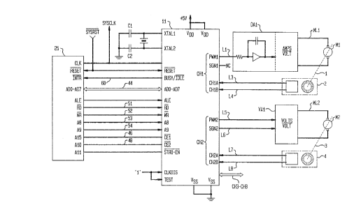
Referring to Fig. l, the MCS ASIC, generally
indicated as 11, is in bus communication with a host
programmable microprocessor, generally indicated as 25. In
t~e preferred ~mhodimsnt, the MCS ASIC 11 has eight (8)
Input/Output (I/0) c~annels, CH1 through CH2, respectively.
It is noted that the only limitation to the number of channels
is the number of available ASIC channel pins available.
Each of the I/O channels of the MCS ASIC includes a
Pulse Width Modulation pin ( PWMl through PWM8 ) and a Motor
Command Direction pin (SGNl through SGN8) for signal output,
and two input channel pins (CHlA through CH8A and CHlB
through CH8B) for signal input. Each channel CHl through
CH2 can be associated with a particular motor for servo
control of the respective motor. For example, channel CH1
may communicate with a motor Ml such that PWMl is in line LI
communication with the input side of a suitable current
driver amplifier (DAl). The driver DA1 is in line MLl
communication with motor M1. When a current driver
amplifier is used MCS ASIC pin SGN1 is not connected. The
motor Ml output shaft, generally indicated as 1, is in
2 0 Q 3 7 ~ ~
-- 5
direct communication with a suitable incremental shaft
encoder, generally indicated as 2 in a suitable manner. The
output of the encoder 2 is communicated to the MCS ASIC 11
through lines L3 and L4 to respective input pins CHlA and
CHlB. Also, as is illustrated with respect to I/0 channel
CH2, pins PWM2 and SGN2 of the MCS ASIC 11 may be in line L5
and L6, respectively, communication with the input of a
suitable voltage driver amplifier voltage amplifier VA1.
The amplifier VAl is in line ML2 with a motor M2. The motor
M2 output shaft, generally indicated as 3, is in direct
communication with a suitable incremental shaft encoder,
generally indicated as 4 in a suitable manner. The
remaining six (6) motors, not shown, are in communication
with respective channels CH3 through CH8 of the MCS ASIC 11
in like manner.
Referring to Figs. 1 and 2, the MCS ASIC 11 contains
an oscillator unit 13, MC bus interface 15, 8 I/0 channels CH1
through CH8, respectively and the control execution unit
comprised of a Decoder/Control 21, Address Generator 23 and
Arithmetic-Logic Unit (ALU) 27. The oscillator unit 13 takes
a 12 MHz crystal signal input and derives from it the
necessary clock requirement for the MCS ASIC 11. The MC bus
interface unit 15 contains the digital logic that allows the
motor controller 25 to access the internal memory of the MCS
ASIC 11 and to start the motor control process. The MCS ASIC
11 can implement eight (8) ser~o controls simultaneously
through its eight (8) separate I/0 c~Annels~ The MCS ASIC 11
also contains a Pulse With Modulator Unit 31 and a Quadrature
Decoder Unit 33 with up/down counter.
To execute the digital control, the MCS ASIC 11 invokes a
data-driven logic that takes coded-data (microcode) ~equence
from the RAM 26 downloaded by the motor controller 25 which
when decoded defines the control algorithm steps for all the
ser~o channels being used. The RAM 26 also contains the
control coefficients and computation data results. The ALU 27
performs the filter computation and features a 16X16 bit
multiplier that
2a~37~t ~
-- 6
produces a 32-bit product and a 32-bit accumulator to
minimize the chance of overflow when summing the products.
There is built-in logic for handling floating-point operands
in twos-complement form. All of the logical elements are
interconnected by a 16-bit data bus 36, an additional 4-bit
negative exponent bus for floating-point data 38, an address
bu~ 44 to index a fully-memory mapped system, and a control
strobe bus 42.
The address generator 23 also contains the necessary
logic to demultiplex the lower address and data from the motor
controller bus 44 (AD0-AD7) with a st~n~ard Address Latch
Enable (ALE) strobe signal. The demultiplexing time (ALE low
to valid A0-A7) is 20ns maximum. The demultiplexer outputs
are made available to the motor controller 25 through the MC
bus interface 15 pins A0-A7 through bus 44.
When the MCS ASIC 11 is not executing the control
algorithm, the MCS ASIC 11 allows its RAM 26 to be fully
memory-mapped into the motor controller address decoding sys-
tem upon activation of enable strobes CEl and CE2 by the motor
controller 25 through lines 46 and 48, respectively. At
this time, the motor controller can access the MCS ASIC
internal memory through its bus 44 using the RD and WR
signals through lines 51 and 52, respectively, when CEl and
CE2 are both in "0" state. Lines 53 and 54 are provided to
the MCS ASIC 11 in order to have up to lk bytes of memory.
However, the MCS ASIC 11 internal control logic organizes
the memory into 8-bit, 16-bit, and 20-bit words, depending
on the data structure of the filter variables, when it
executes the control algorithm. The data structure is
determined in the hardware connection of all addressable
elements in the MCS ASIC 11 to the internal data bus.
Hence, the MCS ASIC 11 has a different internal memory map
when accessed by the motor controller then when external bus
acce~s is allowed, i.e., all address are 8-bit wide. The bus
control defaults to external access upon MC ASIC reset.
The dual bus control mechanism allows the motor
controller to download the control algorithm microcode for
all servo channels prior to issuing the first Start Command
20037()~
during a Servo Cycle, examine the microcode data to check
for integrity, load and modify the desired Filter
Coefficients (FC), ~x~r;ne the Position Feedback (PF) count
value, enable the Feedforward-Path (FP) control and load the
desired Motor Command (MC) value through the FP data,
examine the filter input Position Error (PE) and the Digital
Filter (DF) output, and commence the control algorithm
execution with a Start Command (SC) (refer to Fig. 4).
The number of bytes the motor controller 25 accesses
depends on the data structure of the above data, i.e., a
filter coefficient is a three-byte access while a position
command is only a 2-byte access.
Referring to Figs. 3a, 3b, and 4, generally, the
motor controller 25 performs a control cycle every 1
millisecond. In a manner more fully described,
subsequently, during a control cycle "T" of the motor
controller 25, the motor controller issues a start servo
command at Ts to the MCS ASIC 11 at which point
communication between the motor controller 25 and the MCS
ASIC 11 is inhibited. The MCS ASIC 11 then executes a servo
loop with respect to each motor sequentially. After the MCS
ASIC has performed the servo loops, the motor controller 25
can then access the internal memory of the MCS ASIC 11 in
order to obtain the necessary information for determining
the position command (PC) for each motor and downloading the
PC's to the MCS ASIC 11 during cycle period "Td".
The motor controller 25 issues two types of start
commands at time ''Ts'', the Start-All Command (SC) and
Start-Servo Command (SS). The Start-All Command (SC)
signals the MCS ASIC 11 to start execution of the control
algorithm for all the servo channels being used while the
Start-Servo Command (SC) starts the execution of the control
algorithm of the servo channels specified by the start at Ts
control byte. Upon detection of any start command, the MCS
ASIC 11 enters a locked state by activating the BUSY output
line 60.
The frequency at which the MCS ASIC 11 receives a
start command determines the individual servo channel
~ 3 ~
-- 8
bandwidth. The servo channel bandwidth is determined by the
following motor controller 25 maximum execution times:
- to implement the control algorithm of all servo
channels (maximum of 400us for 8 channels)
- to compute the position commands of all servo
channels for the next sampling instant Tn+l
- to download all position commands to the MCS
ASIC
- to implement other system control tasks.
Since this is a digital control system, the motor
controller 25 must generate the start command at a constant
period, T, in each motor control cycle in order for the MCS
ASIC's digital filter algorithm is to be valid for the motor
control process.
The MCS ASIC ll is permitted to communicate with the
motor controller 25 at any time except when the BUSY output
pin of the MCS ASIC ll is activated, i.e., line 60 is
activated by the MCS ASIC ll. The BUSY pin output is
activated ("l" state) upon decoding a Start Command (SC or
SS) from the motor controller 25. Activation of the BUSY
pin indicates the MSC ASIC ll io using its internal bu~ while
executing the control algorithm. Any access attempted
by the motor controller 25 to the internal memory while in
the busy state is ignored by the MCS ASIC ll. After
executing the control algorithm, line 60 is de-activated,
the BUSY ("0" state) to indicate an idle status during which
the motor controller 25 is allowed to access the MCS ASIC ll
internal memory.
The maximum time the MCS ASIC ll is in the busy state
after a Start-All Command (SC) is determined by the maximum
execution time of an individual servo channel control
algorithm multiplied by the number of servo channels being
used. While the maximum time of the busy state after a
Start-Servo Command (SC) is determined by the maximum
execution time ''TsV'' of the specified servo channel control
algorithm.
Each of the channels, CHl through CH2, operates in
like manner as independent servo channels. Therefor, only
~ .
7 ~ ~
g
one channel CHl will be here described in detail. For the
purpose of clarity, the functional operation of the MCS ASIC
ll channel CHl will be described functionally with specific
reference to the functional system elements illustrated in
the functional diagram shown in Fig. 4.
Associated with each channel CHl through CH8 is a
position command (70) register, feed-forward path motor
command (FPC) register 72, microcode registers 74 and
operation control registers 76. The motor-controller 25
communicates with the respective registers through lines 77
through 80 which lines are constituents of bus 44. As
previously noted, line 60 is provided for informing the
motor controller 25 whether the MCS ASIC is BUSY or IDLE.
When line 60 is not enabled (IDLE) the registers 70, 72, 74
and 76 can be accessed by the motor controller 25 through
respective lines 77, 78, 79 and 80.
The FPC register is in communication with a
feed-forward enabling junction 82 by means of a feed-forward
path tFFP) 82. The output of junction 82 is received by a
motor command (MC) register 84.
The PC register 70 is in direct communication with an
enabling junction 86. Output from the enabling junction 86
is directed to summing junction 88. Encoder 2 (ref. to Fig.
l) signals are filtered by a digital filter at function
block 90. From function block 90, the encoder 2 signals are
directed through the quadrature decoder 92 and up/down
counter 94 to an enabling junction 96. Output from the
enabling junction 96 is directed to a position feedback
(PF) register 98 which is in direct co.,....unication with
the summing junction 88.
The output from the summing junction 88 is
representative of the position error and is directed to the
function block lO0 for digital filtering. The digital
filter output from block lO0 is directed to an enabling
junction llO and therefrom to the enabling junction 82. It
should be appreciated by one skilled in the art that the
tracking accuracy by filter equation can be improved by
increasing the number of product terms with appropriate
~3 7~ ~
-- 10 --
coefficients as a function of microcode instruction. By
changing the microcode instruction, the number of product
terms can be changed to more closely track the series of posi-
tion command~ (motion profile) from the motor controller 25.
In the disabled state, junction 82 directs the digital filter
output to the motor command (MC) register 84. Motor Ml
direction commands (SGN) from the MC register 84, when
appropriate, are directed to the motor driver amplifier
(refer to Fig. 1, CH2). The MC register 89 directs a motor
command to an enabling junction 112. The output from
the enabling junction 122 is directed to a gate 114 to pulse
width modulator (PWM) function block 116 (refer to Fig. 2,
element 31). The output from the PWM function block is
directed to the driver amplifier for the motor M1.
~5 The outputs from the operation control register 76
are a PWM enabling signal directed to the gate 114, a PWM
mode signal directed to the PWM function block 116 (mode
operation of the PWM block 116 is subsequently described), a
FFP enabling signal directed to enabling junction 82 and the
start signal enabling to enabling junctions 86, 96 and 110.
Enabling junction 112 is enabled by the motor controller
Data Output (latch data) from MC register 84.
Referring to Figs. 2 and 4, the Position Command (PC)
generated by the motor controller 25 is a 2-byte integer
downloaded from the motor controller to the MCS ASIC 11 for
each servo channel CH1 through CH8 being used. The position
commands (PC) generated by the motor controller
represents the desired motion profile in discrete position
per time interval T, where the position is in number of
encoder counts and 1/T is the MCS ASIC ll's upper bandwidth
limit. Hence, the PC is the position input to the servo
channel. The channel PC input data stream determines how the
respective motor Ml through M8 move, that is, a constant value
for dPC/T~2 (rate of change in PC with respect to T square)
defines the accel or deccel rate; a constant non-zero value
for dPC/T defines the motion's constant velocity rate; and a
zero value for dPC/t defines a steady-state (holding) mode.
~ .A
, ., .1
7 ~ ~
The motor controller 25 downloads the PC input to the
individual servo channel at a constant time period, T, in
order for a sampled-data to be valid. Therefore,
downloading the PCs for all servo channels precedes any
start command, i.e., Start-all (SC) or Start-servo (SS).
That is, each data stream of PC's downloaded by the motor
controller 2S for the subsequent control cycle.
The Feedforward Path (FP) 82 control allows the motor
controller 25 to bypass the control algorithm result, i.e.,
the digital filter output, and write its desired motor
command value directly to the Motor Command (MC) register 84
of the output channel. A FP control byte is provided to the
operation control register 76 for the control of each
individual servo channel feedforward path (l bit per
channel). When the FFP junction 82 is enabled, the output
channel of the corresponding servo is disconnected from the
digital filter lO0 and connected to its feedforward path.
In this mode, the MCS ASIC ll still continues to execute the
control algorithm but the output channel's MC register 84 is
not updated with the new filter output (DF) lO0, but rather,
updated with the value in the FP register 72 loaded by the
motor controller 25 before the start command.
When the MSC ASIC ll is BUSY, the new Motor Command
(MC) i~ derived from the control algorithm re~ult. The FP
control is transparent to the control algorithm which
simplifies the microcode design of the MCS ASIC ll.
The control algorithm is a sequence of coded-date
instructions that the motor controller 2S downloads to the
MCS ASIC ll's microcode memory area before any first start
command, SC or SS, upon MCS ASIC ll reset. Write-access to
this area is inhibited after the first motor control process
had begun, i.e., receipt of start command, to prevent
inadvertent corruption of the data. The motor controller 25
may examine the microcode to check for data integrity during
the not-busy state of the MCS ASIC ll. A soft Reset (RST)
is necessary to re-download the microcode sequence.
The following discussion on the control algorithm
assumes a minimum ALU design implementation of a single
- ~o~
- 12 -
Multiplier/Accumulator Unit without a subtracter element.
The control algorithm, in general, is a direct form
realization of a digital filter with the following
difference equation:
~ M
g(Tn) = ~ Aj * e(Tn-j) + ~ 8i * g(Tn-i)
j=O i=l
The MCS ASIC 11 implements the above filter using the
following data formats:
g: 16-bit 2's complement (16 binary fractional
places)
A: 16-bit 2's complement (16 binary fractional
places)
e: 16-bit 2's complement (integer)
B: 16-bit 2's complement (16 binary fractional
places)
M: 3 (total of 5 sum-of-product terms)
In particular, the control algorithm implements the
lead-lag compensation~for the digital servo system. Since
the MCS ASIC 11 i8 fully momory-mapped internally and
contain~ only on- (1) Multipli-r/Accumulator (M/A) in the AL~
27, th- microcodo in~truction aet is dosigned to ~ ve data
b-tween th- RAM 26, Input/Output, 33 and 31, respectively, and
the ALU 27. Th- ~equenc- of the microcode inotructions
define~ th- control algorithm for the ~ervo channel. An
algorithm implementation using a ~ingle M/A without a
subtracter i~ given by the following algorithm:
DF(Tn) = [ CO*PC(Tn) ]+[ -CO*PF(Tn) ]+[ Cl*PF(Tn-1) ]
+[ -Cl*PC(Tn-1) ]+t C2*DF(Tn-l) ]
PC(Tn-l) = PC(Tn)
PF(Tn-l) = PF(Tn)
IF Feedforward Path (FP) is enabled
THEN MC(Tn) = INTeger [ DF(Tn) ]
ELSE MC(Tn) =
NEXT SERVO CHANNEL
where:
_- 2û~7~ ~
- 13 -
DF(Tn) =digital filter output at present sampling
instant
DF(TN-l) =digital filter output at least sampling instant
PC(Tn) =position command input at present sampling
instant
PC(Tn-l) =position command input at last sampling instant
PF(Tn) =position feedback input at present sampling
instant
PF(Tn-l) =position feedback input at last sampling
instant
(MC(Tn) =motor command output at present sampling
instant
Relating the above algorithm to the general
difference equation, the variable DF i8 the filter output g:
C0 and C1 are the A coefficients: C2 i8 the B coefficient;
and the term [ PC(Tn-PC(Tn-1)3 is the e input. Therefore,
DF, C0, Cl, and C2 have a data structure of 16-bit mantissa
in 2's complement form and a 4-bit negative exponent, i.e.,
a positive integer from 1 to 16 (O) indicating the number of
binary places to the right of the radix point (fraction),
while the inputs PC and PF have a 16-bit integer in 2's
complement form data structure. The maximum value of the
position feedback PF relative to the position command PC
defines the maximum allowable position error e. Since the
maximum e is dependent on the application, the motor
controller 25 determines the absolute limit value, which
must be less than 32k (e is 16-bit 2's complement form), by
examining the value of PF. The digital filter output DF
mantissa is truncated to its lower byte and scaled by the
output channel when transformed into the corre~pon~n~ motor
command (MC). Note that if the Feedforward Path (FP) control
of the servo channel is enabled by the start command data,
the control algorithm is transparent to it, i.e., hardware
logic inhibits the loading of DF to MC.
The above algorithm requires five (5)
multiplications. The following lead-lag algorithm form,
E(Tn) =[ CO*PC(Tn) ]+[ -CO*PF(Tn) ]
DF(Tn) =[ CO*PC(Tn) ]+[ -CO*PF(Tn) ]+[ Cl*E(Tn-1) ]
+~ C3*DF(Tn-l) ]
~0 E(Tn-l) =E(Tn)
MC(Tn) = INTeger [ DF(Tn) ]
20037~)~
",_
- 14 -
results with only four (4) multiplications where the
variable E is a partial filter output, hence, has the same
data format as DF, i.e., g. Also, Cl has the same format as
C2, i.e., B.
The above algorithms assure that the
Multiplier/Accumulator unit does not have a subtracter
circuitry. Hence, the negative value of the coefficients
are downloaded to the MCS ASIC 11 as well as their positive
values so that the sum of products involving the positive
and negative values of the coefficient produces the
difference function, i.e., the term
[ C0*PC(Tn) ]+t -C0*PF(Tn) ] is really C0*[
PC(Tn)-PF(Tn) or C0*e(Tn) where e is the position error
term.
It is noted that a subtracter element in the M/A unit
I5 directly computes the value of the position error, thus,
simplifying the filter algorithm.
Each servo channel has its own I/O and RAM address,
hence, if no control algorithm uses those addresses, then
the corresponding servo channel is not being used. The
maximum execution time for an individual servo channel
control algorithm is 50us. Therefore, if all eight (8)
servo channels are being utilized, the maximum time for the
MCS ASIC ll's motor control process is 400us. The number of
servo channels utilized and the time the motor controller 25
takes to issue any start command, SC or SS, determines the
upper bandwidth limit of an individual servo channel when
all are in steady-state mode, or, constant position command.
The microcode instruction set is designed to operate
in the MCS ASIC's 11 fully memory-mapped internal
architecture consisting of eight (8) separate pairs of I/O
channels, a single Multiplier/Accumulator, and a single RAM
area for data storage. MOVE and SHIFT commands are used in
order to simplify the MCS ASIC ll's decoding and internal
bus control logic.
The MOVE commands are used to transfer data between
I/O, RAM, and Multiplier/Accumulator registers. Depending
~OQ.~
- 15 -
on the data structure, the data transfer may be 8-bit (for
MC data), 16-bit (for PC and PF), or 20-bit (for DF and
C0-C2) wide. Generally, in all MOVE instructions, the
transferred data may be truncated if the destination word is
smaller than the data, i.e., a 16-bit data moved into an
8-bit register. Therefore, the specific address locations
for these variables vary in width depending on the
corresponding data structure and the connections of all
addressable elements to the internal data bus determines the
significant data. The upper or lower 16-bit of the 32-bit
accumulator result and 4-bit exponent may be moved to any
RAM or output channel address.
If a piece of data is already present in the data bus
(placed by the source), a MOVE command may direct that data
to more than one destination to facilitate transfer of same
data from an input channel to an operand register and/or to
a RAM location, or, from the accumulator to RAM, and/or to
an output channel, and/or to an operand register.
The SHIFT commands are used to position the radix
point of the 32-bit accumulator mantissa, i.e., increments
or decrements the 4-bit exponent value, to move the
significant value of the result into the accumulator's upper
or lower 16-bit area.
A MOVE to the second operand register (20-bit wide)
of the Multiplier/Accumulator starts the multiplication and
summing process. A MOVE to a M/A Clear-Control register
initializes all M/A 4-bit exponent registers to 0S, the
16-bit operand registers to ls, and the 32-bit accumulator
to 0. This prepares the M/A for the next servo channel
control algorithm execution.
The process of multiplying two 16-bit operands and
accumulating the product result is implemented by the
Multiplier/Accumulator (M/A). The 16-bit multiplier
produces a 32-bit product. A separate 32-bit accumulator
sums the products and minimizes the chance of overflow
during multi-cycle operations. The M/A operands and results
data formats are both 16-bit mantissa in 2's complement form
with a 4-bit negative exponent, i.e., a positive integer
~0037()1
- 16 -
from 1 to 16 (0) to indicate the number of binary places to
the right of the radix point (fraction). The 32-bit
product's exponent value is automatically adjusted to 16
binary places, i.e., the 32-bit product is 16-bit integer
and 16-bit fraction. Since the 32-bit accumulator sums the
product, it has the same accuracy as the product term. To
obtain the desired significant value of the accumulator
result, i.e., convert to integer or 2 binary places, the
whole 32-bit can be shifted left or right, incrementing or
decrementing its exponent value, the number of times
specified by the microcode instruction. Only the upper or
lower 16-bit portion of the accumulator and its 4-bit
exponent can be accessed through the microcode instruction.
The multiplication and summing process is started
only by a microcode load instruction to an operand register
of the M/A.
Referring to Figs. 2 and 4, the output stage of each
individual servo is a pulsed-width modulator (PWM) channel.
The MCS ASIC 11 has eight (8) separate PWM output channels
(PWM1 through PWM8). Each PWM channel contains an 8-bit
latch, a free-wheeling counter, and a comparator circuit
that compares the value of the latch and the counter in a
conventional manner. The PWM output port is a logic 1 when
the latch data is greater than the counter data; a logic 0
when the counter data is greater than the latch data.
Each PWM channel has two (2) modes of operation
selectable by the microcode instruction that moves the
filter output DF to the output channel. The first is the
scaled mode (default). The Motor Command (MC) contains a
8-bit latch data. As the microcode instruction moves the
lower 8-bit integer-part of the Digital Filter (DF) output
to the PWM, the input latch circuitry automatically scales
the data byte by adding 128, thus, scaling the MC value to
+/-127. Therefore, the PWM port is at 100% duty cycle when
the latch holds full voltage in one direction; 50~ when zero
drive; and 0% when full voltage in opposite direction
providing 128 discrete units of current value to each servo
channel. In this mode, the PWM circuit upon reset defaults
;~003701
- 17 -
to a 128 value in its MC latch. The second mode is the
absolute mode where the sign (bit 7) of the 2's complement
form filter output DF is placed at the SGN output of the PWM
channel and the absolute value of DF is obtained and loaded
into the motor command MC latch. Hence, in this mode, 0
duty-cycle when the latch holds zero drive and 100% duty
cycle when full voltage at the direction defined by the SGN
output.
The Motor Command (MC) latch is accessible to the
motor controller 25 when the MCS ASIC 11 is in the idle
state. If the Feedforward-Path (FP) control of the servo
channel is enabled, the MCS ASIC 11 inhibits the loading of
the DF output data to the MC latch, allowing the motor
controller 25 computer to directly write its desired motor
command value to the output channel (PWM) when the MCS ASIC
11 goes to idle state.
The input stage of each individual servo channel is a
quadrature decoder and 16-bit up/down counter. The
quadrature decoder samples the two quadrature signals from
the shaft encoder. The 16-bit up/down counter counts every
quadrature state transition-counting upwards when the
channel "A" signal leads channel "B" signal, i.e., 90
electrical degrees out of phase between the two signals, and
counting downwards when channel "A" lags channel "B". A 180
electrical degrees phase shift will result into an undefined
incremental count, i.e., two (2) quadrature state
transition. Input signal filtering is provided for each
encoder channel to discriminate noise in the signal line.
The described MCS system has been described in its
preferred embodiment within a preferred environment which
description should not be viewed as limiting to the
invention. The scope of the invention is set forth in the
claims hereto.