Note: Descriptions are shown in the official language in which they were submitted.
2003846 YJ-7525
;. ~. ' ' ' :
SYNCHRONOUS MULTIPLEX TRANSMISSION APPARATUS
. ~ ~
BACKGROUND OF THE INVENTION
1. Field of the Invention
The present invention relates to a system for
sending and receiving data of the type where frames each
divided into a supervisory data field and information
data field in data format are successively transmitted,
in particular a synchronous multiplex transmission
apparatus, more particularly relates to a receiving unit
in such a synchronous multiplex transmission apparatus.
2. Description of the Related Art
Multiplexing of digital data on a transmission
line is an essential technique for the efficient use of
a transmission medium and economic signal transmission.
In particular, the synchronous multiplexing
15 system proposed in CCITT Recommendation G.707, G.708,
and G.709 multiplexes 50 Mbps unit data in frame units
to enable transmission of several Gbps of data and
enables realization of high speed, large volume data
transmission.
In such a synchronous multiplexing system, as
explained in further detail later, the data is
Y~ transmitted in units of frames consisting of a fixed ~ ~`
~ length supervisory data field and a fixed length -~
y~ ~ information data field. A fixed length unit of
information data is accommodated in the afore-mentioned
information data field. The head position of the
~ information data is indicated by a pointer in the
,~ supervisory data field.
. . .
Further, the CCITT recommendation defines a
3~ stuffing reception in consideration of the slight
deviation between the clock frequency on the trans-
mission side of the data and the clock frequency on the ;~
reception side due to, for example, temperature
fluctuations on the transmission line. In this stuffing
- ~ 35 reception, there is a so-called "negative stuff" wherein -~
, .,~ : , ' . : :
Z0038~6
- 2 -
part of the supervisory data field (1 byte~ is allocated
to part of the information data and a "positive stuff"
wherein unnecessary stuff bits (1 byte), that is, dummy
bits, are added as information data to the information
,~ .
data field.
In the above-mentioned synchronous multiplex
transmission, in the state where no stuff is generated,
the pointer indicates the head position of the
information data, but when the stuff is generated,
information on the type of the stuff, i.e., which of the
~ :. .
negative stuff or positive stuff is generated, is
indicated by the pointer. Therefore, when a stuff is
generated, it is necessary to find the head position of
the information data one frame before and the head -~
position of the information data within the current
frame in accordance with the type of the stuff
generated. Right now there is a demand for a
synchronous multiplex transmission system wherein it is
possible to easily detect the head positions.
f~ O In particular, as explained later, when a -
;~ negative stuff is generated, there are cases in which
the head positions of the two information data in a
frame are simultaneously present, so it is impossible to
find and specify the head position of the information
data effectively. Further, when a positive stuff is
generated, there are cases in which no head position of
the information data exists at all in the frame, so it
also impossible to find and specify the head position of
the information data effectively.
i 30 ~ In a synchronous multiplex transmission
apparatus, in particular in the receiving unit, one of
the important operations is the finding and specifying~
of the head positions of the information data from among
the successive frames being transmitted in. The reason
35 is that unless the head position of the information data ~ ;
can be specified, it is impossible to extract only the --
information data selectively from the successive frames.
2003846
.,... ~
-- 3 --
SUMMARY OF THE INVENTION
The present invention is made in consideration of
this point and has as its object the provision of a ~ :
synchronous multiplex transmission apparatus and a .
5 reception processing method enabling easy detection of `: :~
the head position of the information data using simple
hardware.
To achieve the above object, a synchronous `~
multiplex transmission apparatus of the present
invention having a reception processing unit which
successively receives a plurality of data frames
comprised of pairs of supervisory data fields having a ; . :
fixed byte length Ls and information data fields having :~
a fixed byte length Li, detects the heads of the -
15 information data fields from the data frames received, ~ :
and outputs head detection signals, wherein
the said reception processing unit comprises~
an information data field detection means
which calculates only the term in which the said.~
20 information data fields exist and outputs an enable - ~ -;
signal only during that term; and .
a counting means which outputs the head : ~ :~
detection signal simultaneously with a reset to zero ::
each time the count of a number of bytes equal to the : .- .;:
25 said fixed byte length Li is completed, said counting :.
means continuing the counting operation only in the term
: where said enable signal is output and stopping the
~ counting operation when the said enable signal is not - .::
output,
said information data field detection means - ::
... .
u~J~ comprises:
a first counting unit which successively
counts in byte units all the bytes (Ls+Li) of the said
` data frames received; :
a stuff detection unit which views the .~:
supervisory data fields of the data frames and detects
', ,!: ,
~ if a negative stuff or positive stuff is included in the
.. . .
. .
i ~ .
X~0~3~346
-- 4
said data frames or if no negative stuff and positive
stuff are included; and
an effec-tive information data extraction unit
which extracts only the effective portion of said
information data corresponding to the case where there
is a negative stuff, the case where there is a positive
stuff, and the case where there is no negative stuff and ~
positive stuff based on the results of detection in said ;
stuff detection unit, said enable signal being output
10 from said effective data extraction unit; :
said synchronous multiplex transmission
apparatus has, in addition to said first counting unit,
a second counting unit, which second counting unit : :
constitutes said counting means, operates in accordance
with the said enable signal, and outputs said head
detection signal;
said information data field detection means ~:
further includes a head position detection unit, said
head position detection unit outputting said head .. ; .
detection signal instead of said second counting unit
only when neither of said negative or positive stuff is
detected in the said stuff detection unit, i.e., only .
during normal operation,
said head position detection unit views the ~
25 said supervisory data fields of the data frames .;~
received, detects the head position indicated by the : . .
pointers included in the fields, and outputs said head :::
detection signal when the series of byte numbers in the `~
said data frames and the head positions indicated by : `
30 said pointers match, .. :.~
said first countins unit is comprised of: ~ ::
a frame synchronization circuit which detects ~: .
frame synchronization bytes in said supervisory data
field of said data frames and establishes frame
35 synchronization and :;~
a whole frame counter which successively ~ ~:
counts the series of bytes from the head of said data :~ ;
: ~:
::
^". ".".` '' . ' ' ' ~. . ' '' ' ' , ' ' , '. . ' '
;~00~846
- 5 -
frames detected by said frame synchronization circuit, . :~
said stuff detection circuit comprises: :
a pointer latch circuit which detects said
pointers from the said data frames received and holds
the said head positions indicated by the said pointers;
and
a stuff detection circuit which analyzes the
data pattern of the said head positions held in said
pointer latch circuit and detects if either a negative
stuff or positive stuff is generated when said negative
stuff or positive stuff exists,
said effective information data extraction ~
unit comprises a stuff control circuit, said stuff
control circuit generating said enable signal based on
the series of bytes counted by said whole frame counter
and the results of detection of the said stuff detection
circuit, that is, whether the stuff is negative or :
positive or if there is no stuff, ::
said second counting unit is comprised of~
an information data counter which performs a
count operation in accordance with said enable signal
from said stuff control circuit and
a zero detection circuit which detects zero
when the count of said information data counter becomes
zero due to a zero reset, said head detection signal
being output when zero is detected by said zero :
detection circuit;
said head position detection unit comprises:
a number counter which indicates the byte
30 nuimber of a series of bytes successively counted by said `.
whole frame counter and
a comparison circuit which operates only when
:: one of the said negative and positive stuff is detected
:~ by said stuff detection circuit and detects coincidence
or noncoincidence of the said head position produced
from the said pointer latch circuit and said byte
number, said head detection signal being output from
` :
~ iX..~
Z0038~6
- 6 -
': ~
said comparison circuit and the information data counter
being reset to zero when said coincidence is detected.
BRIEF DESCRIPTION OF THE DRAWINGS
The above object and features of the present
5 invention will be more apparent from the following -
description of the preferred embodiments with reference
- to the accompanying drawings, wherein:
Fig. 1 is a schematic view of the constitution
of a synchronous multiplex transmission system to which
10 the present invention is applied; -; ;
Fig. 2 is a view of the data format of a data
frame received and processed by the present invention;
Fig. 3 is a view of the data frame in one
dimension; -~<r '
Fig. 4 is a schematic view of the state when a
negative stuff is generated; ;~
Fig. 5 is a view of the state when a positive ;
stuff is generated; ~
Fig. 6 is a block diagram of the constituent ` -
20 principle of the present invention; `
Fig. 7 is a timing chart schematically showing
the operating principle of the present invention;
Fig. 8 is a block diagram of one embodiment of
the constituent principle of Fig. 6;
Fig. 9 is a circuit diagram showing much
specifically the constitution of Fig. 8; and -~
Fig. 10 is a detailed view of an example of
the circuits 221, 241, and 261 in Fig. 9. ~ .
DESCRIPTION OF THE PREFERRED EMBODIMENTS
! 30 Before describing the embodiments of the present
invention, the related art and the disadvantages therein
will be described with reference to the related figures.
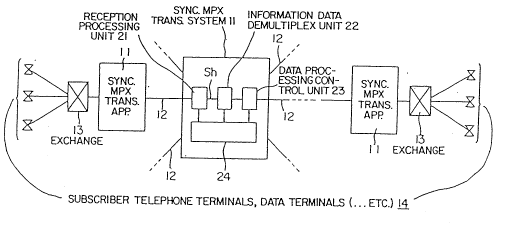
Figure 1 is a schematic view of the constitution of
a synchronous multiplex transmission system to which the ~ ~
35 present invention is applied. In the figure, 11 is a - ` ~`
synchronous multiplex transmission apparatus partic~
ularly relevant to the present invention, which is ~ ~`
20~)3846
-- 7 --
inserted suitable intervals in a long distance
transmission line 12. In the figure, only the central
synchronous multiplex transmission apparatus 11 is shown
in detail. An exchange 13 is also inserted in the
transmission line 12. Communication of information data
is performed among subscriber telephone terminals and
data terminals 14 etc.
Even in the synchronous multiplex transmission
apparatus 11 shown in the center of the figure, only the ;~
reception processing unit 21 is particularly related to
the present invention. The reception processing unit 21
works jointly with an information data demultiplex
unit 22. The other portions include a data processing
control unit 23 and transmission processing unit 24.
Figure 2 is a view of the data format of a data
frame received and processed by the present invention.
The digital data received from the transmission line 12
by the reception processing unit 21 is handled as a
predetermined data frame. The data format of the data
frame is as shown in the figure. Note that the data
format is based on the synchronous transport module 1
(STM1) of the CCITT recommendation. However, in the
figure, mainly the portions related to the present
invention are shown. One data frame DF is formed as a
matrix of M rows and N columns, for example, M=9 and
N=90. This "90" means 90 bytes and is the length in the
case of 52 ~bps. With a transmission line with a higher
degree of multiplexing, for example, 156 Mbps, N=270 (90
x 3) bytes. Therefore, making the explanation in the
3~ case of 52 Mbps, one data frame DF is constituted from a
series of byte groups of 810 (= 9 x 90) bytes. The byte
groups are made of pairs of supervisory data fields
(left side in the figure) and information data field
(right side in the fLgure). In the supervisory data
field, there are a pointer and frame synchronization
bytes Al and A2. Bl and B2 are parity bytes.
The pointer shows the head position of the
.' ~ :" ~ ' - .
X0~)38~6
-- 8 --
information data. The position directly after the
pointer is the head position (byte number = 0). The
information data field is constituted by 783 bytes
(522~782, 0-521) from the byte number 0 to the byte ;~
number 782. The remaining 27 (=810-783) bytes form the ~
supervisory data field. This "27" forms 3 rows x 3 --
columns. At the position of the point may be formed, ~ ;
according to need, a negative stuff Sn and positive ;~ -
stuff Sp related to the present invention.
Figure 3 is a view of the data frame in one ~
dimension. One data frame DF is formed from a pair of - ~ ;
supervisory data field SD and information data field ID.
The field SD is constituted with a predetermined fixed ~ ~
byte length Ls. The field ID is constituted with a ~-
predetermined byte length Li. On the transmission
line 12 (Fig. 1) is successively transmitted a plurality
of data frames DF. These are successively received at
the reception processing unit 21 (Fig. 1). In this
case, the reception processing unit 21 detects the head
of the information data field ID from the data frames
and outputs the head detection signal Sh. The ~
information data demultiplex unit 22 (Fig. 1) executes ~ '
the demultiplex operation based on the signal Sh.
Figure 4 is a schematic view of the state when a ;
negative stuff is generated. The upper portion in the
figure shows any successive three pieces of information
data ID1, ID2, and ID3 out of the series of information
data ID, while the lower portion shows the series of
data frames DF accommodating the data ID1, ID2, and ID3.
Now, assume that the characteristics of the
transmission line change and that the clock frequency
deviates somewhat higher. The upstream side synchronous
multiplex transmission apparatus generates a negative ~ ~
stuff Sn (Fig. 2). Figure 4 shows an example where this -
Sn is inserted in the data frame DF accommodating the
information data ID2. Note that the negative stuff Sh
inserts the head position of the ID2 in the last one
~0C113~3~fi
g
,:
byte (usually a non~used byte) in the above-mentioned
pointer (3 bytes) in the supervisory data field SD.
This being the case, the head detection signal Sh
in the data frame (central data frame) must be issued at
the Sh2 in Fig. 4. I f the negative stuff Sn and a
positive stuff Sp are not generated, that is, in the
normal transmission state, then as shown in Fig. 4
regarding the information data ID1, the head detection
signal Sh is generated such as Sh1 at the position at
the boundary of the field SD and the field ID.
Since a negative stuff Sn is generated at the
information data ID2, the central data frame DF
accommodating the ID2 has its end shifted forward
(direction of left side in the figure) and an empty byte
e is formed. To fill this empty byte, the head of the
next infoDation data ID3 is entered there. Then, the
following supervisory data field SD is jumped and the
remaining data ID3 is received again. This being so, the `
head detection signal Sh for the ID3 must be generated
20 at Sh3 in Fig. 4. As a result, the situation arises -
where two head detection signals (Sh2 and Sh3) are
generated in a single data frame DF.
Figure 5 is a view of the state when a positive
stuff is generated. In particular, it shows an example
of generation of a positive stuff Sp in the information
data ID3 of Fig. 4. This Sp is inserted in the upstream
side synchronous multiplex transmission apparatus due to
changes in the characteristics of the transmission line
(when clock frequency deviates somewhat lower). Note
that the positive stuff Sp is also shown in Fig. 2. Sp
is inserted in the byte directly after the supervisory
;~ data field SD in the form of a dummy bit and does not ~ ~-
have any information. As shown in Fig. 5, in the state
of this figure, the situation occurs where the head
detection signal Sh does not occur even once in the data
frame (center of figure) DF accommodating the
information data ID3.
: -. ::
200~38~fi
, - 10 - ,,
As mentioned above, in a transmission apparatus
using the negative stuff Sn and the positive stuff Sp
for synchronous multiplexing, as explained in the above
Fig. 4 and Fig. 5, the head detection signal Sh occurs ~
5 irregularly. Therefore, in the reception processing ~ -:
unit 21, this irregular state has to be projected and
the timing of occurrence of the head detection signal Sh ~ ~;
adjusted adaptively.
With the current level of technology, it is usually
attempted to contrcl the above adaptive adjustment by a,
for example, microprocessor, using a program. However,
when it comes to high speeds such as 156 Mpbs, the load
on the microprocessor becomes great. Therefore, the
present invention does not rely on the assistance of
such a microprocessor but makes it possible to obtain an
irregular head detection signal at a high speed by -;~
simple hardware. -
Figure 6 is a block diagram of the constituent :~
principle of the present invention. In the figure, 21
and 22 are the afore-mentioned reception processing unit
and information data demultiplexer (DEMUX). The series
of data frames DF received are applied on the one hand
to the demultiplex unit 22 and are applied on the other
hand to the reception processing unit 21. The reception
25 processing unit 21 generates the head detection signal ;
Sh and gives it to the demultiplex unit 22, where the
demultiplex information data Dout is obtained.
The reception processing unit 21 of the present
invention includes an information data field detection
30 means (ID DET MEANS) 31 and a counting means 32. The -
information data field detection means 31 calculates
only the term in which the information data fields ID
exist and outputs an enable signal EN only during that
time. Further, the counting means 32 outputs the head
detection signal Sh simultaneously with being reset to
zero each time it compietes the counting of a number of ~-
bytes equal to the afore-mentioned fixed byte length Li.
Z0038~
-- 11 --
The counting means 32 continues the counting operation
only during the term in which the enable signal EN is
output and stops the counting operation when no enable
signal EN is output.
Therefore, even when the afore-mentioned irregular
head detection signal Sh occurs, it is possible to
automatically generate the head detection signals Shl ,
Sh2 , Sh3 , Sh4 , etc. such as shown in Fig. 4 and ~
Fig. 5 at the respectively specified timings without ~ ;
10 being aware of the irregular state. Further, the -
above-mentioned means 31 and 32 can be realized by a
combination of simple hardware (mentioned later). -~
Figure 7 is a timing chart schematically showing
the operating principle of the present invention. The
figure enables understanding of the reception processing
operation of the present invention. This reception ~;~
processing operation can be expressed as the following
process steps. Before this, however, expressing the
reception processing operation simply, as shown in
Fig. 7, the counting means 32 always carries out a
;~ counting operation in the term when the enable signal EN
i8 generated (that is, the term where an information
data field ID exists) and does not perform the counting
operation at other times (see count pulse CP in Fig. 5). ~ -~
Note that the count pulse CP is equivalent to a byte
expressed by the smallest box in Fig. 2. Every time the
count hits the 783rd (expressed as after 782 in Fig. 2) --~
pulse CP, the head detection signal Sh is generated,
Shl ' Sh2 ~ Sh3 -- These Sh1 , Sh2 , Sh3 .
l ~ 30 are generated without any regard as to the presence or ;;
;~ absence of the negative stuff Sn or positive stuff Sp.
The steps of the above-mentioned reception
processing steps are as follows: a first step of
calculating only the term in which an information data
field ID is present; a second step of counting the
series of bytes in a data frame DF only during the term
calculated in the first step; and a third step in which
2003846
- 12 -
the afore-mentioned head detection signal is output each ;~
time the number of bytes counted in the second step -
matches the number of bytes equal to the fixed length -
Li. Explaining this more specifically, the first step
5 includes a fourth step of counting the series of bytes ~ ~-
from the head to the end of the received data frame DF ;
and a fifth step of division into a supervisory data
field SD and information data field ID by the count at ~ ~
the forth step. More specifically, the fifth step ;
includes a sixth step of detecting pointer in the
supervisory data field SD and a seventh step of ~
analyzing the pointer detected in the sixth step and ~;
judging the generation of the negative stuff Sn, the
generation of the positive stuff Sp, or the nonexistence
15 of the negative stuff and positive stuff Sn, Sp. Even ~; :
more specifically, in the first step, (i) when a -
judgement is made in the seventh step that no negative ~ -
or positive stuff exists, the term from the byte at the
head position designated by the pointer to the byte
equal to the fixed length Li is set as the term; (ii)
when a judgement is made in the seventh step that a
negative stuff Sn is generated, the rising edge of the
term is made faster by exactly one byte from the head ~ `
position designated by the pointer just before; and
2~ (iii) when a judgement is made in the seventh step that
; a positive stuff Sp is generated, the rising edge of the
term is made slower by exactly one byte from the head -
position designated by the pointer just before. No
matter what of the cases of (i~, (ii), and (iii), the
rising period is so controlled that there is no fall
during the term of the information data field ID and
during the term corresponding to the fixed byte length
Li.
Figure 8 is a block diagram of one embodiment of
the constituent principle of Fig. 6. Referring to the
figure, the above-mentioned information data field
detection means 31 includes therein a first counting
'4'i:,'~ j:: - . - . . ~ . ~. . :
Z00384fi
3 --
unit 111 which successively counts in byte units the
total bytes (Ls+Li) of the data frames DF received; a
stuff detection unit 121 which views the supervisory
data field SD and detects if a negative stuff Sp or
positive stuff Sp is included in the data frame DF or if
these negative stuff and positive stuff are not
included; and an effective information data extraction
unit 131 which extracts only the effective portion of
the information data in accordance with the case where
there is a negative stuff Sn, the case where there is a
positive stuff Sp, and the case where the negative stuff
Sn and the positive stuff Sp are not included, based on
the detection results in the stuff detection unit 121.
An enable signal EN is output from the effective
information data extraction unit 131.
In addition to the first counting unit 111, there
is a second counting unit 151. This second counting -;~
unit 151 constitutes the counting means 32 (Fig. 6) and
operates in accordance with the enable signal EN to
output the head detection signal Sh.
The information data field detection means 31
further includes a head position detection unit 141, ~;
which head position detection unit 141 outputs a head
detection signal Sh instead of the second counting ;~
unit 152 only when neither of the negative and positive
stuff Sn, Sp are detected by the stuff detection
unit 121, i.e., only during normal operation.
The head position detection unit 141 views the
supervisory data field SD of the data frames DF
! I3~ received, detects the head position designated by the
pointer included in the field SD, and outputs the head
detection signal Sh when the series of byte numbers in~
the data frame DF matches the head position indicated by
the pointer.
In summary, the first counting unit 111 supervises
all the 810 bytes, for example, shown in Fig. 2. On the
other hand, the stuff detection unit 121 supervises the -
~038~6
- 14 -
pointer of Fig. 2 and supervises further if there is a
negative stuff Sn or a positive stuff Sp. Note that
whether or not there is an Sn or Sp is determined by
analysis of the data pattern of the pointer.
Specifically, a plurality of specific bits in the bit
train of one byte of the pointer are inverted ("0" ~
'l", "1" ~ ~'0") with respect to the corresponding bits
transmitted just before. A first specific bit group is
pre-allotted for the negative stuff Sn, and a second
(remaining) specific group is allotted for the positive
stuff Sp. If there is no inversion in the specific bit
groups, it is the normal case where neither a negative
stuff or positive stuff are generated. The pointer
indicates the head position of the information data -
field.
The effective information data extraction unit 131
outputs the enable signal EN from the head position of
the negative stuff Sn of Fig. 2 when the stuff detection
unit 121 detects a negative stuff Sn. Conversely, it
outputs an enable signal EN from the end portion of the
positive stuff Sp of Fig. 2 when the stuff detection
unit 121 detects the positive stuff Sp. The stuff
detection unit 121 outputs a detection signal Sn (for
example, Sh1 in Fig. 7) directly after the pointer from
the head position detection unit 141 if neither the
stuff Sn or Sp is detected. ~hen the enable signal EN
is output, the second counting unit 151 is driven only
in the term in which the EN exist. In the above
example, each time the counting unit 151 finishes
counting up to ~'782--, a head detection signal (Sh) such
as Sh2 ~ Sh3 , Sh4 , -- in Fig- 7 is output from the
counting unit 151. As explained, the present inventio~
cleverly utilizes the fact that the byte length of the
information data field ID is always constant (=Li)
regardless of the presence or absence of Sn or Sp.
Figure 9 is a circuit diagram showing more
specifically the constitution of Fig. 8. In the figure,
:, :
X(~0~346
- 15 -
the first counting unit 111 of Fig. 8 is constituted by
a frame synchronization circuit 211 which detects the
frame synchronization bytes (Al, A2 in Fig. 2) in the
supervisory data field SD of the data frames DF received
5 and establishes frame synchronization and a whole frame
counter 221 which successively count~ the series of 810
bytes, i.e., the whole frame, from the head (top left
corner byte in Fig. 2) of the data frame detected by the
frame synchronization circuit 211. Therefore, the whole
10 frame counter 221 works as a reference frame clock -~
source of the reception processing unit 21.
The stuff detection unit 121 of Fig. 8 is
constituted by a pointer latch circuit 241 which detects ~ p
the above-mentioned pointer from the data frames DF -~
15 received and holds the head position indicated by the
pointer and a stuff detection circuit 231 which analyzes
the data pattern of the head position held in the
pointer latch circuit 241 and detects if a negative or
positive stuff is generated when a negative stuff Sn or
20 positive stuff Sp exists. Regarding the data pattern,
as already explained, when inversion of a specific bit
group ("0" ~ "1", "1" - "0") is detected, it is known
that a negative stuff Sn or positive stuff Sp is
generated. An example will be shown below.
Assuming that the pointer in the data frame just
before indicates, for example, the pointer value of 1,
for example, a pointer expressed by 10 bits will be as ;~
follows~
p n p n p n p n p n
O O O O O O O O O 1 ( 1)
When it is detected that the pointer received is as
:, ~.:: :
the following (2):
p n p n p n p n p n
0 1 0 1 0 1 0 1 0 0 (2)
the first bit group (n) is bit inverted, so it i5 known
that a negative stuff Sn is inserted in the date frame
DF now received.
- ~ ~. -:
: .~: ' ~';"~'
Z~03846
- 16 -
Conversely, if it is detected that the pointer
received is as the following (3):
p n p n p n p n p n
1 0 1 0 1 0 1 0 1 1 (3)
5 the second bit group (p) is inverted, so it is known ~ ~-
that a positive stuff Sp is inserted in the data frame
DF now received.
Whatever the case, if the stuff Sn or Sp is
indicated by the pointer, the value of the pointer at
10 that time becomes completely meaningless, so the stuff
detection circuit 231 stops the operation of comparison
circuit 251. The reason is that the comparison
circuit 251 operates using a meaningful pointer value
held by the pointer latch circuit 241 as an input. Note
15 that the comparison circuit 251 and the number
counter 223 function effectively under normal conditions
where the stuff Sn and Sp are not generated. An
explanation will be made of these below.
The present invention is particularly beneficial in
20 the case where one of the stuff Sn and Sp is generated,
so the explanation will be made of the portion of the
circuit which functions in such a case.
The effective information data extraction unit 131
of Fig. 8 is constituted of a stuff control circuit 261
25 in Fig. 9. The stuff control circuit 261 generates the
enable signal EN based on the series of bytes counted by
the whole frame counter 221 and based on the detection
results of the stuff detection circuit 231, that is, the
negative stuff or positive stuff or the lack of such
30 stuffs. Note that a detailed example of the stuff
control circuit 261 is disclosed later together with a m
detailed example of the whole frame counter 221.
The second counting unit 151 in Fig. 8 is
constituted, as shown in Fig. 9, by an information data
35 (ID) counter 225 which performs a count operation in
accordance with the enable signal EN from the stuff
control circuit 261 and a zero detection circuit 271
.-;~
200~846 ;: ::
- 17 -
which detects zero when the count equals zero by the
above-mentioned zero reset (explained in Fig. 6). When
a zero is detected by the zero detection circuit 271,
the head detection signal Sh is output. The information
5 data counter 225 may be constituted by a general counter ;~
provided with a count enable terminal. It receives byte
units of pulses from the whole frame counter 221 at the ;
counting input and counts up only during the term when
the enable signal EN exists. However, when a number of
pulses equal to the number of all bytes of the
information data field ID is received, the count returns
to zero. When a signal EN is once again received, the
counting unit counts up again. The zero detection `
circuit 271 which detects if the counts is zero may be
15 realized by a decoder which uses, for example, the `~ -~
- output bit group of the counter 225 as an input. The `-~
~ head detection signals Sh2 , Sh3 , Sh4 .... shown in
;~ Fig. 7 are output from the zero detection circuit 271.
When no stuff pulse Sn, Sp appears (normal times), the
head detection signal, for example, Shl in Fig. 7, is
generated from the circuit portion mentioned below.
Note that when the stuff pulse Sn, Sp does not appear, ``~
~ it means that there are no changes in the charac~
;~; teristics of the transmission line (mentioned earlier)
and further there has been no change of lines. When the
communication traffic is large a bypass route is
selected. When the line is switched to a bypass route,
a large deviation which cannot be adjusted by the stuff
~ pulse Sn, Sp is generated between the transmission side ~ i~
'~ I!, ' ~0 data frame and the reception side data frame. At this
time, the head position of the information data field
must be specified based on the pointer value indicated
by the pointer. This pointer value is held in the
pointer latch circuit 241 (Fig. 9) mentioned earlier
3~ with each arrival of a data frame DF. The held pointer
value and the count value of the number counter 223 are
compared by the afore-mentioned comparison circuit 251.
::~ , . .
200~846
. ~
- 18 -
These circuits correspond to the head position detection ; ~ ~ -
unit 141 of Fig. 8. That is, the head position
detection unit 141 of Fig. 8 is constituted by the
afore-mentioned number counter 223 which indicates the
byte number of the series of bytes successively counted
by the afore-mentioned whole frame counter 221 and the
afore-mentioned comparison circuit 251 which operates
only when either the positive stuff or negative stuff
Sn, Sp has been detected by the stuff detection
circuit 231 and which detects coincidence or noncoin-
cidence of the ID head position and byte number from the --
pointer latch circuit 241. When coincidence is
detected, the head detection signal Sh is output from
the comparison circuit 251 and the information data ~ ;
counter 225 is reset to zero. The ID counter 225 is
reset to zero since if some value remains in the ID -
counter 225 the value becomes erroneous and at the time
when the enable signal EN is next generated, an offset
ends up occurring in the output of the counter 225.
Note that, looking at the number counter 223, it is
possible to use a read only memory (ROM) instead of the
number counter 223. This ROM receives the count output
from the whole frame counter 221 (810 from 0 to 809 in
the above-mentioned example) as the address input. When
the count is a value corresponding to the information
data field ID, according to the afore-mentioned example,
it operates so as to output 0 to 782.
Figure 10 is a detailed view of an example of the
circuits 221, 241, and 261 in Fig. 9. Note that in
30l Fig. 9i, the frame synchronization circuit 211 is; known.
The pointer latch circuit 241 may be realized by a known
shift register, the counters 223 and 225 may be realized
by a known counter, the comparison circuit 251 may be -~ -
realized by a usual digital comparator, and the zero
detection circuit 271 may be realized by a known
decoder, as mentioned earlier, so disclosure of detailed
examples of the same will be omitted.
200384~
Referring to Fig. 10, the whole frame counter 223
of Fig. 9 is constituted by a frame counter 223 which
counts the M x N series of bytes (illustrated in Fig. 2)
constituting the data frames DF having the data format
expressed by M rows and N columns from the head of each
of the data frames DF to the end thereof; a first ~ ;
comparator (COMP I) 224 which detects whether or not the
count of the frame counter 223 matches with a
predetermined byte position (see Sn in Fig. 2) for
insertion of the negative stuff Sn; a second comparator
(COMP II) 225 which detects whether or not the count of
the frame counter 223 matches with a predetermined byte
position (see Sp in Fig. 2) for insertion of the
positive stuff Sp; and a third comparator (COMP III) 226
which detects whether of not the count of the frame
counter 223 matches with a predetermined byte position
(see "INFORMATION DATA" in Fig. 2) for insertion of the
information data. The outputs of the first and second
comparators 224, 225 are applied to the stuff control ;~
circuit 261, while the output of the third compar~
ator 226 is applied to the stuff control circuit 261 and
the number counter 223. ~!r
~` The stuff control circuit 261, as shown in Fig. 10, -~
is constituted by a first gate (AND) 264 which outputs
25' the enable signal EN at the timing when the two
conditions are satisfied that the stuff detection ;
circuit 231 detects the occurrence of the negative stuff
~i~ Sn (Sn DETECTION) and there is coincidence output from
the first comparator 224; a second gate (NAND) 265 which
~ 30' outputs an inhibit signal Si which stops the trans- `
; ~ mission of the enable signal EN at the timing when the
two conditions are satisfied that the stuff detection
circuit 231 detects the occurrence of the positive stuff
Sp (Sp DETECTION) and there is coincidence output from
the second comparator 225; a third gate (AND) 266 which
sends the enable signal EN while coincidence is being ~ : ;
detected with the byte group (ID) by the third
i " ,~ :,, -, ,, ",; " ~ " ~ ,,, ,, " ,": ,,, ,, ~ "", ~ ~ " ~ ; ", j~ ~, ,,,, " ~,,
200~8~fi
.. .
.
- 20 -
comparator 226 and while the inhibit signal Si is not
being output from the second gate 265 (Si = "H"); and a : :
fourth gate (OR) 267 which achieves logical OR of the
outputs from the first gate 264 and the third gate 266 . -~
and uses it as the enable signal EN.
The stuff detection circuit 231 has a first stage - ;
shift register 232 and second stage shift register 233.
The register 232 stores the current pointer and the `~
register 233 stores the pointer of one data frame before
10 supplied from the register 232, EOR gates (EOR) 234
: and 235 detect the presence or absence of the occurrence .
of the already mentioned bit inversion for the fist bit - ;~
group (p), while EOR gates 236 and 237 detect the
already mentioned bit inversion for the second bit
group (n). If there is bit inversion for the first bit
group (p), an Sp DETECTION signal is output from the AND
~:~ gate 238. Conversely, if there is bit inversion for the
~;~ second bit group, an Sp DETECTION signal is output from
the AND gate 239. Unless both the Sp and Sn DETECTION
~r~ 20 signals appear, the output of the AND gate 240 becomes
~ "H" (high) and the comparison circuit 251 (Fig. 9) is ~. . .
;'''5'''~ ~ made active.
;.
. As explained above, according to the present
invention, both the regular head detection signal S
25 shown in Fig. 7 and the irregular head detection signals . - -~
Sh2 , Sh3 , and Sh4 arising due to the stuff Sn, Sp are
automatically obtained by simple hardware without the
aid of a computer.
" .~ , ': .
~, -