Note: Descriptions are shown in the official language in which they were submitted.
-1-
CERAMIC CASED CAPACITOR
BACKGROUND OF THE INVENTION
. This invention relates generally to a novel
ceramic cased capacitor and related methods of
production. M ore. particularly, this invention relates
to a ceramic cased capacitor having a high temperature
operating capability, together with a high lead pull
strength and substantially improved resistance to
moisture penetration to avoid moisture induced
failures.
Ceramic dielectric capacitors in general are
well known in the art for use in a wide range of
electronic circuit applications, for example, for use
as a charge storage device, a circuit coupling or
decoupling device, a filtering ~ device, etc. Such
capacitors conventionally comprise at least two
conductive plates encased in facing relation at a
predetermined spacing or gap within a selected
dielectric casing material, typically such as a ceramic
based material formulated to have a selected dielectric
constant. With this construction, the capacitor has a
charge storing capacity which is a function of the
overlapping or "active" plate surface areas, the
thickness of the dielectric material defining the
interplate gap (dielectric thickness), and the
dielectric constant of the casing material within the
gap. In many electronic circuit applications,
particularly in aerospace operating environments, it is
desirable to , provide a highly compact capacitor
i~~~~~~~~.
construction with a relatively high capacitance. In
this regard, multiple layer capacitors have been
developed with two groups of conductive plates of
opposite polarity arranged alternately in a stack and
encased within the selected dielectric casing material,
with the multiple plates providing a significantly
increased active plate surface area with a relatively
small overall increase in capacitor size. See, for
example, U.S. patents 3,235,939 and 3,456,313.
In the past, ceramic dielectric capacitors have
been produced by formulating the selected dielectric
material such as a barium titanate or the like into
relatively thin sheets. While in a relatively flexible
"green" state before firing, the ceramic sheets are
electroded ar silk-screened with a refractory metal to
define thin conductive plates of selected area. A
plurality of these ceramic sheets with conductive
plates thereon are laminated into a stack and then
fired to form the sheet into a rigid and dense,
substantially monolithic casing structure having the
conductive plates encased therein at a predetermined
dielectric thickness. The conductive plates are shaped
to provide thin edges exposed at the exterior of the
casing for connection to appropriate conductive leads
as by solderin g or the like. In multiple plate
capacitors, groups of the plate edges are appropriately
coupled to each other by conductive metallization
strips applied to the exterior of the casing, with the
conductive leads being fastened to the metallization
strips by soldering or the like.
A variety of problems and disadvantages have
been encountered in the use of ceramic dielectric or
monolithic capacitors of the general type described
above. More specifically, the externally exposed edges
cif the encased conductive plates define entry sites
along so-called knit line defects for ingress of
moisture between the conductive plates and adjacent
dielectric material. Such moisture ingress
i~~r~ ~~~~.
_3_
contributes to internal dendritic growth or increased
ionic mobility which causes corresponding reductions in
insulation resistance between adjacent conductive
plates; which can lead to parametric or catastrophic
failure. Moreover, thermal cycles encountered during
normal capacitor operation can cause repeated
vaporization and, recondensing of minute. moistures
quantities, resulting in cracking and failure of the
ceramic dielectric material. Still further, in a
conventional ceramic capacitor, the externally formed
solder joints used to connect the conductive leads
sometimes provide inadequate mechanical lead pull
strength especially at elevated operating
temperatures. The external solder joints are also
esthetically unacceptable and/or require insulation
coverings for some circuit applications.
In the past, the problems of moisture
penetration have been addressed primarily by
encapsulating the entire monolithic casing within a
jacket or coating of a suitable insulating material,
such as an epoxy, potting compound, polymeric coating,
etc. This jacket or coating is intended to seal the
casing against moisture penetration, while
simultaneously covering solder joints ~o enhance the
appearance of the capacitor. Advantageously, the outer
jacket additionally provides mechanical support for the
conductive leads to increase the lead pull strength.
However, the outer insulation jacket inherently
increases the overall size and shape of the resultant
capacitor, resulting in a failure to optimize the
capacitance per unit volu me, sometimes referred to as
volumetric efficiency. Moreover, while the jacket
provides some resistance to moisture penetration,
moisture ingress may nevertheless occur by penetration
between the jacket and the conductive leads, or by
gradual migration directly through the jacket in
r~~r~ x~ ~~..
-4-
accordance with the bulk permeability of the jacket
material. Alternately, different thermal coefficients
of expansion for the jacket and casing can result in
moisture laden air being sucked in by the jacket when
significant thermal cycles are encountered. When such
moisture penetration occurs, delamination of the jacket
from the ceramic casing often results in reduced
insulation resistance, or short circuiting high voltage
corona between the casing and the jacket. The
differential- -thermal coefficients can also cause
cracking failure of the ceramic casing as the jacket
and casing expand and contract at different rates in
response to high temperatures or thermal cycling
operation. Attempts to minimize risk of such cracking
failure have focused upon the use of resilient jacket
materials which, unfortunately, do not provide
acceptable mechanical support for the conductive leads.
Encapsulated monolithic casing capacitors are
also limited to environments of use wherein outgassing
of solvents and other volatiles can be tolerated. That
is, encapsulating materials exhibit outgassing
characteristics in 'varying degrees, wherein a gradual
mass loss over a period of time is encountered as
solvents and/or other condensable volatiles are
outgassed to the surrounding environment. Such
outgassing is unacceptable in some capacitor
applications, such as in space and other sensitive
environments.
There exists, therefore, a significant need for
improvements in ceramic dielectric capacitors,
particularly with, respect to providing enhanced
resistance to moisture penetration without the use of a
conventional encapsulating outer jacket. Moreover,
there exists a need for such improvements in a
capacitor designed for substantially optimized
volu metric efficiency and relatively hig h lead pull
~~s~ i~~~:~..
-5-
strength. The present invention fulfills these needs
and provides further related advantages.
STJMMARY OF THE INVENTION
In accordance with the invention, a novel
ceramic cased capacitor and related method of
construction are provided, wherein the capacitor is
substantially impervious to moisture penetration and
provides a high lead pull strength capable of operation
at relatively high temperatures. The capacitor
includes at least two conductive plates encased at a
selected gap within a monolithic casing of a selected
dielectric material. Conductive leads are attached by
soldering lead ends within shallow recessed seats
formed in the casing, with each seat being lined
partially by the conductive plate or plates to be
coupled to the associated lead. This recessed seat
mounting arrangement provides an attractive and
mechanically superior lead attachment site without the
use of an encapsulating insulative jacket or coating,
whereby moisture penetration problems associated with
such jackets or coatings can be avoided.
In a preferred form of the invention, a multiple
layer ceramic capacitor is' formed by applying the
conductive plates of a refractory metal individually as
thin layers onto a plurality of ceramic sheets in an
unfired, green state. The conductive plates are
defined by two sets of plates of different polarities,
and the ceramic sheets are arranged in a stack with the
two plates in alternate sequence. The conductive
plates are formed with their outer marginal edges
disposed inboard relative to outer edges of the ceramic
sheets. One or more ceramic base and cover sheets are
placed at the top and bottom of the stack. The
assembled stack is then laminated by appropriate heat
2004241.
_6_
and pressure and then fired to form the ceramic sheets
into a densified substantially monolithic core or
casing having the conductive plates encased therein in
parallel with interplate dielectric thickness of
predetermined size.
The two sets of conductive plates are shaped to
define outwardly projecting tabs disposed for
connection to the conductive leads. More particularly,
the first plates include vertically aligned tabs which
extend beyond adjacent margins of the second plates,
and vice versa. The recessed seats for mounting of the
conductive leads are formed as shallow counterbores
bridging respectively into the aligned edges of th a
tabs on the first and second plates. In a preferred
process, the recessed seats are drilled subsequent to
lamination of the stack but prior to densification
firing. These recessed seats are lined with an
app ropriate conductive glass frit material, which is
fired in place. The lead ends are then anchored as by
soldering within the recessed seats in electrical
contact with the first and second plate groups,
respectively. The resultant capacitor provides superior
lead pull strength and lead attachment appearance
without requiring an outer insulation jacket or
coating, and wherein the attachment site of the leads
to the casing is substantially impervious to moisture
penetration. The omission of the encapsulation jacket
beneficially permits the capacitor to be used at
relatively high operating temperatures, relatively high
voltages, and/or subjected to significant thermal
cycling with reduced risk of failure.
In operational use, the first and second groups
of the conductive plates are connected via the leads
for opposite polarity. In one form of the invention,
the groups of first and second plates are formed for
attachment of the conductive leads at a common side of
2004241.
_,_
the ceramic casing, thereby providing a so-called
radial capacitor geometry. In another form, the plates
are configured for lead attachment at opposite ends of
the casing to provide a so-called axial capacitor
geometry.
Other features and advantages of the present
invention will become more apparent from the following
detailed description, taken in conjunction with the
accompanying drawings which illustrate, by way of
example, the principles of the invention.
BRIEF DESCRIPTION OF THE DRAWINGS
The accompanying drawings illustrate the
invention. In such drawings:
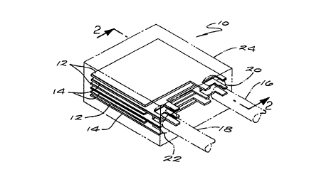
FIGURE 1 is a perspective view illustrating a
radial leaded monolithic ceramic cased capacitor
embodying the novel features of the invention;
FIGURE 2 is an enlarged longitudinal vertical
sectional view taken generally on the line 2-2 of
FIG. l:
FIGURE 3 is an exploded perspective view of the
ceramic cased capacitor;
FIGURE 4 is a perspective view similar to FIG. 1
and illustrating a monolithic ceramic casing with
encased conductive plates, and including recessed seats
for secure attachment of conductive leads; ...
FIGURE 5 is an enlarged fragmented sectional
view illustrating one of the recessed seats formed in
the ceramic casing;.
FIGURE 6 is fragmented sectional view similar to
FIG. 5 and depicting application of a glass frit
material to the surfaces of the recessed seat;
FIGURE 7 is a fragmented sectional view similar
to FIG. 6 and showing firing of the glass frit
material;
~~Q4~~1.
_8_
FIGURE 8 is a fragmented sectional view similar
to FIG. 7 but illustrating solder attachment of a
conductive lead within the recessed seat; and
FIGURE 9 is a perspective view similar to FIG. 1
but illustrating an axially leaded monolithic cased
capacitor embodying one alternative preferred form of
the invention.
DETAILED DESCRIPTION OF THE PREFERRED EMBODIMENTS ,.
As shown in the exemplary drawings, a novel
ceramic cased capacitor referred to generally in
FIGURE 1 by the reference numeral 10 is designed for
secure electrical and mechanical attachment of a
plurality of encased conductive plates 12 and 14 of
opposite polarity to a pair of conductive leads 16 and
18, respectively. The ends of the conductive leads 16
and 18 are anchored within recessed seats 20 and 22
formed in a substantially monolithic core or casing 24,
' and in a manner such that the capacitor is
substantially impervious to moisture penetration.
The ceramic cased capacitor 10 of the present
invention is constructed in a manner providing a
substantially optimized volu metric efficiency, namely
high charge storing capacity in a highly compact, space
efficient size and shape. The invention provides an '
apparatus and method for securely anchoring conductive
leads in electrical communication with the conductive
pl~.tes 12 and 14 while safeguarding against undesired
moisture penetration which can cause premature
capacitor failure. The leads are attached to the
capacitor casing 24 in a manner providing superior lead
pull strength without addition of a conventional outer
insulating jacket or coating formed from an epoxy or
potting compound, polymeric material, etc. As a
result, the capacitor formed in accordance with the
2004241.
_g_
invention can be operated at high operating
temperatures such as at 260°C (about 550°F) and higher
without significant risk of temperature induced failure
or disconnection of the conductive leads. The omission
of the conventional encapsulating outer jacket improves
overall longevity and reliability by eliminating
jacket-associated failures such as delamination of the
jacket from the casing, high voltage corona between the
jacket and casing, differential thermal coefficients of
expansion with respect to the jacket and casing,
reductions in insulation resistance due to moisture
penetration, and/or dendritic growth.
As shown in FIGS. 1-5, the ceramic cased
capacitor 10 comprises at least one conductive plate 12
and at least one conductive plate 14 encased in spaced
parallel relation within the ceramic casing 24. The
illustrative drawings depict a preferred multiple layer
capacitor having multiple plates 12 and a corresponding
number of the plates 14 arranged within the ceramic
casing 24 in an alternating stack. For example,
FIGS. 1-5 specifically show three of the conductive
plates 12 interleaved in spaced relation with three of
the conductive plates 14. As will be described, the
sets of conductive plates 12 and 14 are electrically
connected, respectively, to the conductive leads 16 and
18 of opposite polarity which are adapted in turn for
connection to a voltage source of an electric circuit
' (not shown). In use, the sets of plates 12 and 14
function to store an electrical charge, with the charge
storing capacitance (in farads) being a function of the
overlapping (actives plate areas, the dimensions of the
gaps between the plates, and the dielectric constant of
the casing material disposed within the interplate
dielectric thickness.
The capacitor 10 is constructed by formation of
the conductive plates 12 and 14 upon a plurality of
casing material sheets 26, as viewed best in FIG. 3.
2a~441.
-lo-
These casing sheets 26 are formulated to have a
selected dielectric constant, with a ceramic material
such as barium titanate being commonly used. The
precise material formulation is adjusted as is well
known in the art to provide a particular selected high
to low dielectric constant. The thus-constructed
sheets 26 are then processed preferably in a flexible
green or unfired state to apply the conductive
electrode plates 12 and 14 thereon. As is known in the
art, these plates 12 and 14 are normally applied as
metallized films using printing or electroding
techniques wherein conductive inks containing an
appropriate refractory metal or metals are applied. In
a preferred form, the plates 12 and 14 axe applied as
lattices to permit improved bonding of the casing
sheets 26 during subsequent processing. Importantly,
the marginal edges of the conductive plates 12 and 14
are spaced inboard from the marginal edges of the
sheets 26.
The casing sheets 26 are assembled in a stack
(FIG. 3) with the conductive plates 12 and 14 arranged
in alternating sequence. Lower and upper base and
cover sheets 27 are assembled below and above the
sheets 26 to provide added material thickness, wherein
the cover sheets 27 do not carry conductive plates
thereon. The assembled stack is then laminated under
appropriate heat and pressure, volatiles are eliminated
in the course of a conventional binder bake-out step,
and thereafter the stack is subjected to a conventional
sintering or densification firing step to fire the
sheets and form the substantially monolithic casing 24
(FIGS. 2 and 4). Within this rigid and densified
monolithic casing 24, the conductive plates 12 and 14
are suspended in fixed parallel relation with
interplate dielectric thicknesses of predetermined
dimension.
200441.
-11-
The conductive plates 12 and 14 are shaped to
define outwardly projecting tabs for connection
electrically and mechanically to the conductive leads.
More specifically, the conductive plates 12 are
identically shaped to define short tabs 28 which are
generally vertically aligned with each other and
protrude outwardly relative to adjacent margins of the
other plates 14. Similarly, the conductive plates 14
include a generally vertically aligned set of short
tabs 30 extending outwardly relative to adjacent
margins of the plates 12. FIG. 3 illustrates the
formation of these tabs 28 and 30 to terminate inboard
relative to the outermost margins of the casing 24.
Moreover, FIG. 3 illustrates these sets of tabs 28 and
30 extending outwardly from their respective plates in
laterally spaced relation at a common side of the
casing.
Subsequent to formation of the laminated casing
24, the pair of recessed seats 20 and 22 are formed to
protrude inwardly from the exterior surface or envelope
of the casing. As shown in the illustrative drawings,
these recessed seats 20 and 22 comprise a pair of
shallow round counterbores formed by drilling or the
like to bridge short distances, respectively, into the
edges of the aligned groups of tabs 28 and 30. In a
preferred process, the counterbores are drilled after
lamination of the stack of Sheets 26 and 27, but prior
to final densification firing. Alternatively, the
counterbores can be formed by ultrasonic drilling or
the like subsequent to densification firing. As shown
in FIGS. 4 and a,~the resultant recessed seats 20 and
22 expose edges of the conductive layers 12 and 14
within a limited region lining interior surfaces of the
seats. The diametric sizes of the seats are chosen for
relatively close reception of the conductive leads 16
and 18, as will be described, and to permit substantial
exposure of each tab of the associated set of
conductive plates.
200424.
-12-
Preparatory to lead installation, and subsequent
to firing of the casing 24, the recessed seats 20 and
22 are lined with a selected conductive frit material
applied typically in paste form, as viewed in FIG. 6.
Although the precise formulation of the frit material
may vary, a silver or palladium-silver glass powder
composition in paste carrier is preferred. The silver
component provides high quality conductive coupling to
the conductive J.ayers exposed within the recess 20 or
22, whereas the glass component bonds well with the
adjacent surfaces of the ceramic casing 24 in a manner
providing substantial imperviousness to moisture
penetration. Such bonding of the glass material to the
interior surfaces of the recesses is obtained by
subjecting the casing and frit material (FIG. 7) to
appropriate heat within a furnace, sometimes referred
to as a silver kiln. This heating step, typically at a
. temperature of about 750--800°C (about 1380°-1440°F)
causes the glass material to glaze and at least
partially penetrate the surrounding ceramic material
for excellent bond therewith. The actual thickness of
a resultant glazed frit layer 34 is relatively thin,
but is shown in exaggerated thickness in the
accompanying drawing for purposes of clarity.
The ends of the conductive leads 16 and 18 are
then seated and soldered into the recessed seats 20 and
22, with the frit material and addition of sufficient
solder providing a conductive yet hermetically sealed
connection with the casing. As shown in FIGS. 2, 4 and
8, a preferred end geometry for the conductive leads 16
and 18 comprises a Dumet style configuration wherein a
conductive lead of copper clad nickel or the like
includes a slightly enlarged, cylindrical and coaxially
formed head 33 at the end thereof. The lead head 33 is
sized diametrically to fit closely but with at least
some tolerance into the assaaiated recessed seat 20 or
22 to permit at least some thermal size variation
2~0~2~1.
-13-
without pulling loose or unduly stressing the ceramic
casing 24. For example, an approximate diametric
difference between the recessed seat and the lead head
33 of about 5-10 mils is sufficient for most
applications.
In a preferred solder process, the conductive
leads are manipulated and soldered in place using
resistance tweezers 36, such as the resistance tweezers
marketed by American Electrical Heater Company of
Detroit, Michigan under the name American Beauty, and
model nos. 105-83 (power unit), 105-41 (tweezers), and
105-19 (foot switch). The tweezers 36 are used to grab
the conductive lead near the lead head 33, as shown
with respect to the lead 16 in FIGS 2 and 8. The
supported lead head 33 is inserted fully into the
associated recessed seat 20 and appropriately energized
to reflow one or more ring-shaped solder preforms 32
placed onto the lead 16 immediately behind the head
33. As shown in FIG. 8, this step is carried out with
the recessed seat 20 presented upwardly, such that the
melted solder preforms 32 flow down about and
substantially fill the annular gap between the head 33
and the frit layer 34. This soldering process is
advantageously facilitated by preheating of the
capacitor and the lead to a point close to the solder
reflow temperatu re, whereby minimal additional heat
and/or time is required by operation of the resistance
tweezers 36. Moreover, soldering is further
facilitated by preliminarily dipping the lead head 33
in an appropriate flux bath and then into a molten
solder bath before placement into the recessed seat.
The assembled capacitor and leads are then cooled in a
controlled manner to avoid undue thermal stress.
The resultant ceramic cased capacitor 10 thus
supports the conductive leads 16 and 18 in a secure and
stable manner, and with attractive and clean solder
joints. The recessed mounting of the leads at
2004241.
positions buried within the envelope of the capacitor
casing 24 provides extended cylindrical surface areas
for attachment to the leads yielding a high lead pull
strength sufficient to permit the leads to be
manipulated, bent, etc., as required for capacitor
installation and operation even at high temperatures
without significant risk of the leads pulling loose.
Standard epoxy coatings and the like used
conventionally with ceramic cased capacitors can be
omitted, due to the substantially impervious nature of
the casing 24 and the hermetically sealed lead
attachment sites of extended surface areas. This
construction beneficially permits the capacitor to omit
entirely the conventional prior art outer coating,
resulting in a smaller overall size and shape for
greater volu metric efficiency and prolonged operational
life with enhanced performance characteristics. This
omission of the traditional outer coating further
permits facilitated capacitor mounting, for example, by
direct attachment of the ceramic casing to a supporting
substrate. Moreover, the capacitor can be used at high
operating temperature, or be subjected to repeated
thermal cycling without failure. Furthermore,
outgassing from a conventional outer jacket or
degradation of a conventional outer jacket under
hostile environmental condition are avoided.
The novel ceramic cased capacitor farmed
according to the invention may be constructed in a
variety of different geometric configurations to suit
different operating requirements. For example, FIGS.
1-8 show the conductive leads 16 and 18 extending from
a common side edge of the casing 24, thereby providing
a so-called radial capacitor geometry. Alternately, as
viewed in FIG. 9, a similarly constructed capacitor 10'
may include sets of conductive plates 12' and 14'
connected to conductive leads 16' and 18' extending
outwardly from opposite ends of a ceramic casing 24',
thereby defining a so-called axial capacitor geometry.
2004241.
-15-
Various additional modifications and
improvements to the ceramic cased capacitor of the
present invention will be apparent to those skilled in
the art. For example, alternative lead attachment
techniques can be used, such as plated terminations,
nickel barrier terminations, gold terminations, etc.
Further, appropriate leads such as silver-based
materials or the like can be attached without soldering
by the use of silver paste and application of
sufficient heat in a silver kiln. Further, alternative
recess geometries may be utilized, if desired.
Accordingly, no limitation on the invention is intended
by way of the foregoing description and the
accompanying drawings, except as set forth in the
appended claims.