Note: Descriptions are shown in the official language in which they were submitted.
2Q0~48~
COMPUTER WITH IMPROVED
KEYBOARD PASSWORD FUNCTIONS
The present invention relates to digital computer systems, and more
S particularly relates to control of a computer input/output device.
A computer usually contains valuable, confidential or otherwise
restricted information in its memory and/or external storage devices, so it is
accordingly desirable to control access to this information to prevent
unauthorized use. Such controlled access to computer data may be realized
either by providing physical (hardware) means for preventing the use of I/O
devices on a computer system, or by providing software means for restricting
access, such as a routine that confirms a user's knowledge of a password
before granting that user access to information contained in the computer
system.
It is also necessary to restrict user input to a computer from a
keyboard is when the computer is functioning as a "network server",
coordinating communication between multiple computers, terminals and/or
other devices by a local area network (LAN). When functioning as a
network server, a computer is dedicated to the execution of network software,
in order to provide efficient, uninterrupted service to numerous network
devices. If the keyboard of a network server is not disabled when the
network operator is not present, an unrestricted user could potentially gain
~.2oo44s5
-2_
access to normally restricted files, or cause network communication to be
disrupted.
One commonly-used method for restricting user interaction with a computer is
to
provide a "password lock" function in the keyboard or auxiliary device
controller which
can prevent communication between the external devices and the computer.
Typically,
when a controller is in "password lock mode", no communication between
external input
devices and the computer is allowed unless a password is first entered to
remove the
controller from "password lock mode". One type of computer having this
password lock
function is the IBM PS/2 desktop models. If such a function is implemented in
a
peripheral device controller of a computer, however, it may prevent proper
execution of
software which requires communication with the locked-out external devices.
For
example, operating system software may require information about which devices
are
present in a computer system in order to determine the current system
configuration.
Other software that requires application-specific hardware, such as a "mouse",
a digitizing
tablet, or some other specialized data acquisition device, may not function
properly if it
cannot determine whether such devices are actually present in the system.
Accordingly the present invention seeks to provide improved functions for an
auxiliary device controller, particularly a mode of operation which
selectively allows or
restricts communication between a computer and auxiliary devices. Further the
invention
seeks to provide an improved lock-out mode of operation for a computer, but
nevertheless
allow selected functions to be performed while in this lock-out mode.
Accordingly, the invention in one broad aspect provides a method of operating
a
computer system of the type having a CPU and memory associated therewith and a
peripheral controller device coupled to the CPU, comprising the steps of
switching the
peripheral controller device between (i) a normal operating mode wherein the
peripheral
controller device sends unsolicited information to the CPU and the CPU sends
unsolicited
information to the peripheral controller device without reference to password
data and (ii)
a lock-out mode wherein the peripheral controller device cannot send
information to the
CPU unless password data previously stored in the memory associated with the
CPU is
first entered to cause a switch back to the normal operating mode, but the CPU
can send
information to the peripheral controller device and monitoring unsolicited
information
transferred from the CPU to the peripheral controller device when the
peripheral
controller device is in the lock-out mode and selectively allowing only
preselected
r 2004485
-2A-
information transferred to the peripheral controller device by the CPU to
activate the
peripheral controller device for selected functions without switching from the
lock-out
mode.
Another aspect of the invention pertains to a method of operating a computer
system of the type having a CPU and memory associated therewith and having a
peripheral controller coupling a peripheral device to the CPU, comprising the
steps of
switching the peripheral controller between a normal operating mode wherein
the
peripheral device exchanges unsolicited commands and data with the CPU without
reference to password data and a lock-out mode wherein the peripheral device
cannot send
commands and data to the CPU until password data has been entered to cause a
switch
back to the normal operating mode and monitoring unsolicited conunands and
data
transferred from the CPU to the peripheral controller for transfer to the
peripheral device
when the peripheral controller is in the lock-out mode and selectively
allowing only
preselected commands and data to be transferred to the CPU from the peripheral
device
in response to requests from the CPU directed to the peripheral device.
Still further the invention pertains to a computer system comprising a CPU
accessing memory via a system bus and executing instructions fetched from the
memory
to perform operations on data stored in and recalled from the memory, a
peripheral
controller device coupled to the system bus and accessed by the CPU, the
peripheral
controller transferring data and commands to and from the CPU according to a
control
sequence and at least one peripheral device coupled to the peripheral
controller, the
peripheral device generating data and commands for transferring to the CPU via
the
peripheral controller. The control sequence includes a lock-out mode
preventing the
peripheral controller from transferring the data and commands from the
peripheral device
to the CPU but allowing the CPU to transfer selected commands from the CPU to
the
peripheral device.
Typically, the interface between the CPU of a computer and a
peripheral I/O device is implemented using a standard controller or
microprocessor
device for the buffering, translation, or formatting of data as it is
exchanged between the CPU and peripheral devices. One such controller device
is a part number 8042, Universal Peripheral Interface 8-bit Slave
2004~8~
-3-
Microcontroller, manufactured by Intel Corporation, Santa Clara, CA. This
microprocessor or microcontroller includes a ROM or EPROM storage area
(e.g., two-kilobyte) for holding customized machine language instruction
routines that enable the controller to support various commands that it can
S receive from either the controlled device (i.e. a keyboard, a mouse or the
like) or from the main computer processor (CPU). That is, in typical desk-
top computers, the controller device (such as the 8042 device) is itself a
processor, executing the machine language instructions to define a command
sequence, although the same functions could be performed by a state machine
or the like. Use of the 8042 type of device is much less costly and easier to
design, however.
In a "password lock mode", as implemented in standard desk-top
computers marketed today, a peripheral controller device (such as the 8042
type) does not allow any communication between the main processor and the
controlled I/O devices. According to one embodiment of the present inven-
tion, however, the controller (via its ROM or EPROM code) is programmed
to recognize certain commands and responses that should be allowed to pass
between the main processor and a controlled device, even when the controller
is in "password lock mode". Normal user input from the controlled devices
is still restricted however, except for the cases of these selected
command/response sequences. In this way, a user is still prevented from
gaining unauthorized access to files or from disrupting the operation of a
network server, but software which requires communication with external
devices can still operate properly.
Accordingly, an important feature of the invention is for a central
processor to be able to communicate with "disabled" peripheral devices on a
discriminate basis. That is, to distinguish between solicited and unsolicited
responses when a peripheral device sends asynchronous streams of data. In
the example embodiment, the peripheral device or controller is an 8042
,.~ 2Q~4485
-4-
device, but the feature is useful as well in systems employing peripheral
circuitry constructed of logic using gate arrays or the like.
The novel features characteristic of the invention are set forth in the
appended claims. The invention itself, however, as well as other features and
advantages thereof, will be best understood by reference to a detailed descrip-
tion of a specific embodiment, when read in conjunction with the
accompanying drawings, wherein:
Figure 1 is an electrical diagram in block form of a computer system
which uses features of the invention;
Figure 2 is an electrical diagram in block form of the CPU of the
system of Figure 1;
Figure 3 is an schematic representation of the memory management
scheme used in the CPU of Figure 2;
Figure 4 is an electrical diagram in block form of internal details of
a controller chip which may be used in the system of Figures 1 and 2;
Figure 5 is a timing diagram of voltage or events vs. time for read and
write cycles performed by the CPU to access the controller 11 of Figures 1,
2 and 4; and
Figure 6 is a logic flow chart of a program for keyboard input and
keyboard lock-out in the system of Figures 1-4 according to an embodiment
of the invention.
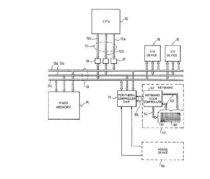
Referring to Figure 1, a digital computer system which may use
features of the invention is illustrated. This system includes a CPU 10 which
in a preferred embodiment is an Intel 80386 32-bit microprocessor, or an
-$-
Intel 80386SX 32-bit microprocessor with 16-bit external data bus; according
to the invention, a peripheral controller device 11 is used to interface the
CPU with a keyboard or mouse. The microprocessor or CPU 10 is connected
by a local bus 12 to a system bus 13 which logically connects the various
components of the system, including the peripheral controller and CPU. If
a 80386 CPU chip is used, the local bus 12 and the system bus 13 include
thirty-two address lines 12a or 13a, thirty-two data lines 12b or 13b and a
number of control lines 12c or 13c. On the other hand, if an 80386SX device
is used, the address busses 12a and 13a are 24-bits, and the data busses 12b
and 13b are 16-bits wide. Also present in the system is a main memory
module 14 which is in a logical address space of 4-gigabytes for an 80386 or
16-Mbytes for an 80386SX, although usually about 1- or 2-Mbyte is physical-
ly present. The system also includes a plurality of other input/output (I/0)
devices 16, such as video display devices, network adapters or modems, and
disk drives, for providing facilities for user interaction with the system, or
for
providing additional bulk-storage facilities for the system. The busses 12 and
13 can be controlled by different devices, at the same time; the processor 10
can be accessing a ,cache controller or numeric coprocessor (not shown) on
the local bus 12, while a disk drive operated by one of the controllers 16 is
transferring data to the main memory 14 using DMA. Although an 80386
microprocesssor is given as the preferred CPU device, it is understood that
other microprocessor devices may make use of the features of the invention,
such as Motorola's 68020 type devices, or later generations of 80386 or 68029
devices; the class of processor devices known as RISC microprocessors may
also employ the concepts herein set forth.
The local bus 12 is separated from the system bus 13 by buffers or
latches 17 for the addresses and data and a bus controller 18 for the control
lines. In this manner, addresses and data are not applied to the system bus,
even though present at the CPU output, unless the controller 18 has received
the proper commands and has ownership of the system bus. Likewise, data
on the system bus is not allowed onto the local CPU bus until the controller
200485
-6-
sees the proper commands from the CPU. In this manner, the CPU 10 can
communicate with other devices on the local bus 12 without tying up the
system bus 13.
Referring to Figure 2, the CPU 10 of the 80386 or 80386SX type used
in the illustrative embodiment is a high performance microprocessor including
an on-chip memory management unit providing virtual memory support. The
microprocessor is of the microcoded type, using "pipelining" or overlapped
instruction execution, and generally includes an execution unit 20, an
instruction unit 21, a memory management unit 22, and a bus interface unit
23. The internal data paths are 32-bit for either device, but the 80386SX has
a 16-bit external data bus 12b while the 80386 has a 32-bit external data bus
12b.
The execution unit 20 performs arithmetic and logic operations on
operands and addresses fetched from memory 14. The execution unit includes
a register file 24 containing a number of general purpose 32-bit registers for
holding operands, results or addresses, a 32-bit wide ALU 25 for performing
the arithmetic or logic operation defined by an instruction, a multiply/divide
circuit 26 for executing instructions using multiply or divide, and a barrel
shifter 27 for executing 0-to-64 bit shifts on data being inputted to the ALU.
Microinstructions stored in a control ROM 28 define the operations
performed in the execution unit. The microinstruction routines are selected
by an entry point derived from the current instruction and applied to an input
29, and the microcode sequence within a routine is determined by a
sequencer 30, based upon a microaddress produced by the last microinstruc-
tion and conditions within the processor. Control signals produced by a
microinstruction are applied to the execution unit 20 via bus 31, and to the
other units of the CPU chip via internal control bus 32.
The instruction unit 21 functions to fetch and decode instructions of
the instruction stream. A prefetch unit 33 outputs addresses via bus 34
.... 200448 i
-7-
through the memory management unit 22 to the external address bus 12a, and
receives instructions back via external data bus 12b and bus 35, to fill an
instruction queue 36 with the next sixteen bytes in the instruction stream,
based upon an instruction pointer in the register file 24. An instruction
consists of an opcode of one or two bytes, usually followed by one or more
bytes of mode specifiers, address displacements and/or immediate data, so an
instruction can be from one byte to six or eight or more bytes in length A
decode unit 37 receives instructions from the queue 36, decodes the opcodes
to generate entry point addresses for the control ROM 28, and determines
what bytes are specifiers, displacements or immediate data and transfers the
appropriate information to other units of the processor; this decode is three-
deep, i.e., the next three decoded instructions are being processed at one
time. This instruction unit is where the I/O instructions used to access the
peripheral controller 11 are recognized upon being initially decoded.
The memory management unit 22 of the CPU 10 of Figure 2 includes
a segmentation unit 38 and a paging unit 39. A 32-bit logical address
produced on bus 40 by the execution unit 20 is translated by the segmentation
unit 38 into a 32-bit linear address on bus 41, and then translated into a 32-
bit physical address on bus 42 by the paging unit 39. Referring to Figure 3,
the segmentation unit 38 adds the logical address on bus 40 to a base address
from segment descriptor registers 43; one of the descriptor registers 43 is
selected by the contents of a segment register 44. The segment discriptors
contain not only the base address for the segment, but also the limits of the
segment (its size) and the level of protection. The sum of the logical ad-
dress on bus 40 and the base address for the segment, if the limit and
attribute checker 45 in the segmentation unit finds the address to be proper,
becomes the linear address on bus 41. If paging is disabled, this linear
address passes through the paging unit 39 without change and becomes the
physical address on bus 42. If paging is enabled, the linear address is first
tested to see if the page address is found in a page cache 46 (a set
associative translation lookaside buffer); bits 13-31 of the 32-bit linear
address
,... 2Qi04~$5
_g_
are compared to the thirty-two most recently used page addresses stored in
the cache 46, and if a match is found the page address for this entry is
forwarded to an adder 47 which produces the physical address on bus 42
using the page address and the lower 12-bit offset from the linear address.
If the page is not found in the cache 46 (the hit rate is perhaps 98%), the
page must be looked up in a page directory 48 and a page table 49 which
are stored in memory 14. The upper 10-bit part of the 32-bit linear address
is used to select 1-of 1024 entries in the page directory 48, producing the
base
address of the page table 49, then the next 10-bit part of the linear address
is used to select 1-of 1024 of the entries of this page table, producing the
translated page address used as an input to the adder 47 as before. The
page entries have protection bits, similar to the segment entries, so several
modes of protection are available. The segmentation and paging units 38 and
39 are used to translate addresses to memory 14, but not I/O addresses,
however, so when the peripheral controller 11 is addressed to transfer
commands or operands it is always at a fixed physical address in the I/O
space.
The bus interface unit 23 includes an address driver 51 functioning to
generate the 24-bit or 32-bit address on external bus 12a along with the byte-
enable bits BEO-BE3 (for 80386 devices, not 80386SX) which are part of the
control bus 12c. When a new valid address is driven onto the bus 12a, an
address status line ADS# is asserted in the control bus 12c. The outgoing
addresses may be pipelined if a next-address signal NA# is asserted in control
bus 12c by an external device; instead of waiting until a Ready line is
asserted to produce the next address, a pipeline control circuit 52 produces
a new address every cycle from the driver 51 if it has received the NA#
signal. All incoming and outgoing data is controlled by multiplexer/transcei-
vers 53 connected to the external data bus 12b. Data to or from the
execution unit 20 is coupled to the transceiver 53 via bus 54, or instruction
stream data to fill the queue 36 is coupled from transceiver 53 via bus 35.
Interrupts and bus arbitration are handled by a request prioritizer 55 which
2004485
-9-
receives HLDA, IIVTR, NMI, ERROR# and BUSY# signals from the control
bus 12c, and generates HOLD signals to the control bus 12c. Definitions of
these control bus signals are contained in Table A.
The microprocessor of Figure 2 is pipelined in that during a given
machine cycle several instructions are executing at various stages at the same
time. An instruction loaded to the prefetch queue 36 in one machine cycle
will be decoded in the unit 37 in the next machine cycle, generating a
microinstruction output from the control ROM 28 in a third cycle, causing the
execution unit 20 to perform some operation in a fourth cycle, then the result
is written to a register of the file 24 in a fifth cycle. Of course, execution
of
other instructions overlap this instruction.
In the embodiment of Figure 1, the interface with the keyboard or
auxiliary device uses a peripheral controller which is an Intel 8042 Universal
Peripheral Interface, a microprocessor device commercially available from
Intel Corporation. This controller is used to implement the interface between
the host processor 10 and two external devices, namely an alphanumeric
keyboard 57, and a mouse 58. The interface between the keyboard 57 and
the microprocessor or controller 11 consists of lines 59 which include a
serial
data line and a single control line called TESTO which is an input to the
controller 11 indicating when the keyboard has data to send. Likewise, the
interface between the mouse 58 and the microprocessor 11 consists of a
similar set of lines including a serial data line and a TESTl line which
indicates when the mouse has data to send.
The peripheral interface microprocessor 11 has 8-bit data in and data-
out registers, and certain control lines, connected to the shared system bus
13.
The host processor 10 communicates with the keyboard 57 via an I/O port;
that is, a specified address in the 1/O address space of the processor 10 is
reserved as a data port used for communication between the CPU 10 and
with the keyboard 57. When the host processor 10 executes an I/O read or
2U0~~~35
-lo-
write instruction to the keyboard's I/O address, a decoder detects this
address
on the system address bus 13a and causes the microprocessor 11 to be
selected and activated, sending or receiving commands or data on data bus
13b via the 8-bit data-in and data-out registers of the microprocessor 11.
For example, the command from the host processor 10 which causes the
microprocessor or controller 11 to enter "password lock mode" is issued via
the data-in register. An applications program executed by the CPU 10
initially asks the user to select a password, and this password is stored by
the
CPU 10 in RAM, so thereafter upon entering a proper keycode sequence the
user can place the system in lock-out mode, at which time the CPU sends the
command to the controller 11 via a data-in register.
Referring to Figure 1, the keyboard 57 includes a key matrix 60
consisting of rows and columns of keyswitches 61. In a typical desktop
computer there would be perhaps 101 keys on the keyboard. A keyboard
controller device 62 performs the function of determining when a key is
depressed and which key is depressed. The column lines of the matrix are
connected to one set of ports 63 of the controller 62, and the row lines are
connected to another port 64; a definition of which key is down is available
from the row and column information at these ports 63 and 64. The
controller 62 is a microprocessor device having a program stored in ROM or
EPROM, like the controller 11; usually a microprocessor device such as
commercially available under the part numbers 8051 or 8048, manufactured
by Intel Corporation, is used for this controller 62. The stored program
performs the function of scanning or polling the keyboard matrix 60 and
generating an 8-bit keycode for each key as it is depressed. These keycodes
are buffered in a 128-byte RAM within the controller 62, and are transferred
to the peripheral controller 11 upon request, and thus to the CPU 10. The
controller 62 generates a TESTO input to the controller 11, then the
controller 11 sends a command back to the controller 62 when ready to
receive keycode data. The keyscan or polling thus goes on independently of
and transparent to the CPU 10 and the peripheral controller 11, but when a
--. 20048
-11-
key is depressed and a keycode is ready to be sent from the controller 62,
the controller 11 and then the CPU 10 are in control of the transfer.
Referring now to Figure 4, the peripheral controller 11 is shown in
more detail. This device is a processor executing instruction code stored in
an internal ROM or EPROM 65 of about 1K- or 2K-byte, and has a 128- or
256-byte internal RAM 66, an 8-bit wide ALU 67 and an 8-bit internal bus
68. Instructions are fetched from ROM 65 using a program counter 69 for
addressing, and loaded into an instruction register 70 then decoded by
instruction decoder 71 which generates control signals to define the operation
of the device. The two inputs of the ALU are loaded from an accumulator
register 72 and a temporary register 73, both coupled to the internal bus 68.
The RAM 66 contains a register file, stack and data storage, and is addressed
by a decoder 74 and multiplexer 75, also coupled to the internal bus 68.
Two 8-bit I/O ports 76 and 77 connected to output terminals of the device
are coupled to the internal bus 68, and are loaded and unloaded under
instruction control. The interface to the CPU 10 uses a pair of data buffers
78 and 79 and a status register 80, all three of which are coupled to an 8-
bit data I/O port 81 which is connected to the system data bus 13b. The
data bus buffer registers 78 and 79, referred to as DBBOUT and DBBIN, are
loaded or read by the controller 11 from the internal bus 68, by executing
instructions from ROM 65; loading or reading these data bus buffers from the
CPU 10 is controlled by lines of the control bus 13c connected to controller
82. These control lines include a write control WR, a read control RD, chip
select CS and address line A0, as defined below. The TESTO and TESTl
inputs 83 and 84 to the chip are connected to conditional branch logic cir-
cuitry 85, which produces an input to the decode and control circuitry 71 and
82 when a conditional branch instruction is executed. The conditional branch
logic 85 also receives inputs representing ALU operation such as carry,
contents of accumulator 72 equal zero, etc., as well as the condition of the
data bus input and output buffers 78 and 79. An 8-bit timer or event counter
circuit 86 is connected to count clock cycles (divided by thirty-two), or to
' '° 2Q0448~
-12-
count external events by an input from the Testl pin, and also produces an
output to set a timer flag which is testable by the conditional branch logic
85
so that a branch instruction can be conditional upon overflow of the counter
86. Also, overflow of the counter 86 generates an interrupt by input to the
decode and control circuitry 71, 82, which is enabled or disabled under
program control. The counter register 86 may be loaded from or to the
accumulator 72 via the internal bus 68. The processor 11 is synched to the
host CPU 10 by clock inputs 87 to a timing circuit 88, and produces a synch
output 89 to the keyboard controller 62, so both of these peripheral proces-
sors 11 and 62 are synched by inputs from the main processor 10. The
controller 11 of Figure 4 executes the instruction set of Table B (as well as
other instructions not material to the present invention).
Referring to Figure 5, a bus cycle is illustrated in which the CPU 10
writes a command or data to the data input register 78 of the controller 11.
During the first Clk cycle, t0, the address strobe ADS# is asserted on bus 12c
by the CPU 10 along with the control signals M/IO# and W/R# indicating
this to be a write to I/O space; AO and certain other address bits are driven
high by the CPU 10 on bus 12a and detected at an address decoder for the
controller 11 at input CS#, indicating the address of the register 78 in I/O
space. Data is driven onto bus 12b by the CPU 10 during the period tl-t2.
Assuming the system bus is free, this write request is asserted or "posted"
onto the system bus 13; the CPU 10 does not wait for any acknowledge that
the write operation was completed, but instead continues with another cycle.
Also shown in Figure 5 is a read cycle, where the CPU performs a read of
the I/O address where the data bus buffer 79 is defined to reside. During
t5, the ADS#, M/IO#, A0, and chip select CS# are the same as for a write,
but the W/R# signal on bus 12c is low, initiating a read operation. By
external logic (not shown) the W/R# signal on control bus 12c and 13c is
converted to separate W# and R# controls for the controller 11. Again,
assuming the bus 13 is free, this read request is asserted onto bus 13 at the
same time as it reaches bus 12. In t6, the I/O control 82 in the controller
200448
-13-
11 recognizes the read request and drives the data onto the output 81 during
t7 and t8. The logic circuit which generates the separate R# and W#
controls also generates a Ready# response to the CPU 10, since the
controller 11 does not produce this signal.
Referring to Figure 6, a logic flow chart, in simplified form, of a part
of an example of a program which may be stored in the ROM 65 and
executed by the controller 11 is illustrated. In an idle state, the controller
11
polls the TESTO and TESTl inputs 83 and 84 and the status register 80 in
a loop to see if there is a keyboard or other auxiliary device (such as a
pointing device, typically a mouse) input, or if the CPU 10 has written to the
data bus input buffer 79, as represented by the decision points 91, 92 and 93
of the flow chart; this loop is implemented using the instruction set of Table
B, in known manner. If the TESTO input is active at point 91, the program
checks to see if the lock-out mode is activated at decision point 94, and if
yes
the sequence returns to the original loop at point 92, since the keyboard is
to be ignored. If lock-out is not activated, then the controller 11 enters a
loop where it reads its port P10 (one bit of the ports 76 and 77) for a count
of eight and loads and shifts these bits to a register of RAM 66 as
represented by the elements 95 of the flow chart. A table look-up is
performed at point 96 to see if the 8-bit word read in is a valid key code; if
not, the original polling loop is re-entered, or if so then a code conversion
is done at point 97 to produce the key codes used by the CPU 10, and the
status of the data bus output buffer 79 is checked at point 98, and if empty
this buffer 79 is loaded at point 99, and port terminal P24 (of I/O ports 76,
77) is set at point 100 to produce an interrupt 1:N1'R input to the CPU 10,
by way of a standard interrupt controller chip, not shown. This interrupt will
cause the CPU 10 to enter a routine to read the buffer 79 using a cycle as
in Figure 5. Although not illustrated here, the controller 11 can buffer
several key codes in RAM 66 if the CPU 10 does not immediately respond
to the interrupt; in some cases the CPU program will mask the keyboard
interrupt while another task is being performed, e.g., refresh of the DRAM
2004485
-14-
chips of main memory. After signalling the interrupt, the controller 11
returns to the polling loop at point 91. The polling loop has a similar input
routine for the mouse input TESTl as indicated at points 92 and 101. Data
input to buffer 78 is found by checking status at point 93, and if true then
at point 102 the data is moved to RAM 66 and the status of the lock-out
mode is checked at point 103; if not in lock-out mode then the data is
interpreted to see what action is needed as indicated by point 104, so if the
input from the CPU 10 is a command then the required action is taken
before return to the polling loop at point 105. If in lock-out mode, however,
the input word is checked at point 106 to see if it is an allowed activity in
lock-out. If not, the input is ignored and the polling loop is re-entered at
105; if so then the usual interpretation and execution are performed.
Whenever a command is sent to the controller 11 via its I/O data
buffer 78, the controller program will respond by sending either an
"acknowledge" code (ACK) or a "resend" code (RESEND) to the CPU via
buffer 79, and possibly more data., depending on the command that was sent.
When in the conventional "password lock mode", however, the controller 11
would not respond to any command, nor would it allow any communication
to or from the keyboard 57 or mouse 58. Such complete disabling of
auxiliary device communication prevented application software running on a
computer in "password lock mode" from determining what type of keyboard
or auxiliary devices were attached, or even whether the keyboard or auxiliary
devices were present or functioning properly.
With the keyboard/auxiliary device controller of the present invention,
however, the following classifications of information transfer are allowed,
even
when the computer is in "password lock mode":
-commands from the host processor 10 to the interface
controller 11;
-commands from the host processor 10 to the keyboard
57 via the interface controller 11;
2004485
-ls-
-commands from the host processor 10 to the auxiliary
device s8 via the interface controller 11;
-solicited responses (only) from the microprocessor or
controller 11 to host processor 10;
s -solicited responses (only) from the keyboard 57 to the
host processor 10 via the interface controller 11; or
-solicited responses (only) from the auxiliary device s8 to
the host processor 10 via the interface controller 11.
In the preceding list, which is implemented in a table in the ROM 6s
, referenced at point 106 of the flow chart of Figure 6, notice that
unsolicited
or user-initiated information transfer from the keyboard s7, auxiliary device
s8, or the processor 11 are not permitted when "password lock mode" has
been enabled. By limiting the transfer of information to the classes listed
above, user interaction with the system 10 is restricted as in conventional
is "password lock mode", while internal system activity can proceed as if
"password lock mode" were not enabled.
A keyboard/auxiliary device controller with functions in accordance
with features of the present invention is defined by the machine-language
code stored in the internal one- or two-kilobyte ROM or EPROM memory
6s of the microprocessor 11. These features reflect modifications of the code
which has previously been used for keyboard functions in systems using the
hardware elements of Figures 1, 2 and 4. The features can be grouped into
three general areas: (1) modifications to the support of controller 11
commands sent from the host processor 10, (2) modifications to the support
2s of communication between the controller 11 and the keyboard s7, and (3)
modifications to the support of communication between the controller 11 and
the mouse s8.
2004485
-16-
(1) Modifications to controller 11 command support: According
to one embodiment of the present invention, commands sent from the host
processor 10 to the controller 11 operating in the improved "password lock
mode" are executed exactly as they would be when the controller 11 is not
operating in "password lock mode", with the following exceptions:
(a) - LOAD PASSWORD COMMAND: If the con-
troller 11 is already operating in "password lock mode", the loading of
another
password is not permitted. Issuance of this command by the host processor
is typically followed by the transfer of password bytes from the processor
10 10 to the controller 11. In "password lock mode", however, these bytes are
transferred from the CPU 10 to the controller 11 and acknowledged by the
controller 11, but then discarded, i.e., not used to overwrite the password
bytes already in the RAM 66.
(b) - ENABLE SECURTTY COMMAND: If the con-
troller 11 is already operating in "password lock mode", re-entering this mode
is not useful and is therefore not pernvtted.
(c) - AUXILIARY DEVICE AND KEYBOARD INTER-
FACE TEST COMMANDS: Since the auxiliary device (mouse) 58 and
keyboard 57 are effectively disabled when the controller 11 is operating in
"password lock mode", issuance of either the Auxiliary Device Test or
Keyboard Test Command causes a code to be returned to the host processor
10 which indicates that the tests have passed successfully, even though no
such test is made, so the host processor 10 will not hang up by waiting
indefinitely for a response.
(2) Modifications to support of communication with the
keyboard 57: As noted above, the keyboard is accessed by the
host processor via I/O reads and writes to the address reserved as the
keyboard I/O port. According to the example embodiment of the present
invention, commands can be issued by the CPU 10 to the keyboard 57 (via
controller 11), and corresponding responses are returned to the host proces-
sor 10, but keystrokes typed on the keyboard 57 are not transferred via
controller 11 to the host processor 10. This is accomplished by providing the
2~~~48
-17-
controller 11 with information (in its ROM code) regarding the keyboard
command structure, so that only the correct number of response bytes are
permitted to be transferred from the keyboard 57 through the controller 11
to the host processor 10. This is done by testing input commands against a
table of permitted commands. Furthermore, a time limit is placed on the
response from the keyboard, and no additional bytes are passed after this
time. The following examples illustrate how these techniques are used to
prevent user-initiated information transfer between the keyboard 57 and the
host processor 10:
(a) - READ KEYBOARD ID COMMAND: The con-
troller 11 excepts a three-byte response from the keyboard 57 when this
command is issued by the host processor 10: the ACK byte, followed by
$(AB), followed by $(83). No more than three bytes are permitted to be
transferred to the host processor 10 after issuance of this command.
(b) - RESET KEYBOARD COMMAND: The controller
11 expects a two-byte response from the keyboard 57 when this command is
issued by the host processor 10. Since resetting the keyboard 57 can take up
to one second, (longer than the typical response time limit accepted by the
controller 11), the controller 11 will wait for an appropriate amount of time
for this response.
(c) - SELECT MODE COMMAND: This command is
issued in two bytes, and can be used in two different ways. The host
processor 10 can issue this command to the controller 11 to cause the
keyboard 57 to enter one of three different operating modes, or it can issue
this command to determine which mode the keyboard is currently in. When
the controller 11 receives the first byte of a SELECT MODE command
destined for the keyboard 57, it forwards the byte to the keyboard 57, then
waits for the second byte of the command. If this second byte is a zero,
indicating a mode query, then the controller 11 expects and permits a two-
byte response, consisting of an ACK byte, and a current mode byte. If the
next command byte is non-zero, however, indicating a "change mode
200448a
-18-
command", then only one response byte, an ACK byte, is expected and per-
mitted.
All other commands issued by the processor 10 to the keyboard 57 are
assumed to have a one-byte response, and the controller 11 permits only a
single byte to be transferred from the keyboard 57 to the processor 10, and
only if it is sent within the required time limit. Otherwise, the controller
11
generates an error byte to the host processor 10 as it would in "non-password
lock mode".
(3) Modifications to support of communication with auxiliary
device: Like the keyboard 57, the auxiliary device 58 can respond
with either
an ACK or RESEND byte for each command sent to it. The number
of
additional response bytes sent from the auxiliary device 58,
however, cannot
be predicted as with the keyboard responses, since a variety
of auxiliary
devices may be attached to the controller 11. In order to allow
communication with the auxiliary device 58, yet not allow the
device to
initiate the communication on its own, the controller 11 depends
upon the
"packetization" of responses from the auxiliary device. When
a command is
issued to the auxiliary device 58 from the host processor 10,
the controller 11
is programmed to expect the response bytes to be sent continuously
until the
auxiliary device 58 has completely replied to the command.
The "packet" of
response bytes is thus accepted by the controller 11 until
a pause is
encountered, at which time the controller 11 stops allowing
bytes to be
transferred to the host processor 10. In this embodiment of
the invention, a
pause is defined as an interval of perhaps about a millisecond
in which no
bytes are sent from the auxiliary device. As with the KEYBOARD
RESET
COMMAND, the AUXILIARY RESET COMMAND can require additional
time (up to several seconds, for example) before making a response.
The
controller 11 accordingly waits an appropriate amount of time
for responses
from AUXILIARY RESET commands, although any other command to
the
auxiliary device 58 is allotted the normal command response
timeout interval
in which to make responses. After this interval, the controller
11 stops
2004485
-19-
accepting response bytes, and generates an error code to the host processor,
as it would if "password lock mode" were not enabled.
The modified behavior of the peripheral controller 11 is realized, as
noted above, by changing the ROM-based code in the controller 11 itself.
No additional variation from the conventional hardware implementation of
keyboard/auxiliary device is necessary in order to realize a controller 11
which conforms to the above-described embodiment of the present invention.
Alternate or additional command/response patterns for the keyboard or for
various auxiliary devices ROM-based code for the controller 11 may be
employed; the foregoing are merely examples.
From the above detailed description of a specific embodiment of the
present invention, it will be evident that improvements to the conventionally
used keyboard/auxiliary device controller have been disclosed which provide
for restriction of user interaction with a computer system while
simultaneously
maintaining non-interference with certain internal system activities which
require communication through a controller in "password lock mode".
While this invention has been described with reference to a specific
embodiment, this description is not meant to be construed in a limiting sense.
Various modifications of the disclosed embodiment, as well as other embodi-
ments of the invention, will be apparent to persons skilled in the art upon
reference to this description. It is therefore contemplated that the appended
claims will cover any such modifications or embodiments as fall within the
true scope of the invention.
200448 i
-20-
TABLE A - CONTROL BUS
M/IO#, D/C#, W/R# and LOCK# are cycle definition signals, setting
forth the type of cycle the CPU 10 is executing on the bus 12. M/IO#
selects a memory reference if high, or an I/O reference if low. D/C# says
whether the access is for data (if high) or for code (if low); this signal can
be used to differentiate between accessing instructions and accessing data.
W/R# is the write/read control, specifying a write operation if high or a read
operation if low. Lock# forces a condition where the CPU 10 maintains
control of the bus 12 and cannot be interrupted by another master.
ADS# is an address status signal, and indicates that new address and
cycle definition information is available on the bus 12a and 12c; this signal
begins every external access by the CPU 10.
READY# is a transfer acknowledge input to the CPU and terminates
a cycle on the local bus 12 by signalling to the CPU 10 for a read cycle that
the data on the bus 12b is ready to be latched into the CPU or that a write
has been completed or posted. Every CPU bus cycle must end with
READY# asserted.
NA# is the next-address request, used to initiate address pipelining by
indicating that the system is prepared to accept new values of address, byte
enable, and cycle definition, even if the end of the current cycle has not
been
acknowledged on READY#.
HOLD and HLDA are bus arbitration signals, where HOLD is asserted
as an input to the CPU 10 when another device requires control of the bus,
and the CPU 10 asserts hold-acknowledge HLDA when it relinquishes control
of the bus in response to HOLD.
INTR is a maskable interrupt request input to the CPU, and when
asserted the CPU executes an interrupt acknowledge cycle in which an
interrupt vector is latched into the CPU from the data bus 12b.
Clock Clk2 is the same clock for both the CPU 10 and the controller
11, and is divided by two internally to produce the internal clock Clk. In the
2UU~1~8
-21-
example, the Clk frequency is perhaps 20-MHz, so the Clk2 frequency is 40-
MHz.
BEO#-BE3# are Byte Enable signals defining which ones of the four
bytes in the 32-bit doubleword on data bus 12b being accessed are wanted by
S the CPU 10. These signals are used in the 80386, but not in the 80386SX.
TABLE B - The Instruction Set:
The controller 11 of Figure 4 executes the following instruction set:
ADD: There are three types of ADD instructions - ADD A,Rr = add
one of the registers Rr of the register set in the RAM 66 to the contents of
A, the accumulator 72; ADD A,@Rr = add the contents of a location in the
data memory part of the RAM 66 selected by register Rr to contents of the
accumulator 72; ADD A,#data = add an immediate value in the instruction
itself to the contents of the accumulator 72. All three of these ADD
instructions also can be with a carry when the mnemonic is ADDC.
ANL: There are three types of AND instructions, like the ADD
instructions - ANL A,Rr = perform an "AND" function of a register Rr with
the contents of the accumulator 72, result to accumulator; ANL A,@Rr =
same for a data memory location, and ANL A,#data = same for immediate
value.
ORL: Again, three types of OR instructions - ORL A,Rr = OR the
contents of a register with the contents of the accumulator, result to
accumulator; ORL A,@Rr = same for a data memory location, and ORL
A,#data = same for an immediate value.
XRL: Exclusive OR instructions are of three types just like the ORL
instructions - XRL A,Rr = Register, XRL A,@Rr = data memory, and XRL
A,#data = immediate.
INC A: Increment the accumulator 72. Also, INC Rr is increment the
register Rr, and INC @Rr is increment the data memory location pointed to
by the contents of register Rr.
DEC A: Decrement the accumulator 72. Likewise, DEC Rr is
decrement the register Rr.
,,.~ 200448a
CLR A: Clear the accumulator 72.
CPL A: Complement the accumulator.
SWAP A: Swap 4-bit nibbles contained in accumulator.
RL A: Rotate accumulator left; also there are rotate right, and
rotate left and right through carry, instructions.
IN A,Pp: Input Fp, a selected one of the ports 76 or 77, to A, the
accumulator 72.
OUT A,Pp: Output the accumulator A to a selected one of the ports
76 or 77, Pp.
ANL Pp,#data: Perform an AND function between immediate data
and a selected one of the ports 76 or 77, result to the port.
ORL Pp,#data: Perform an OR function between immediate data and
a selected one of the ports 76 or 77, result to the port.
IN A,DBB: Input the data bus buffer 79 to the accumulator 72 and
clear the input buffer flag IBF in register 80.
OUT DBB,A: Output the contents of the accumulator 72 to the data
bus buffer 78 and set the output buffer flag OBF.
MOV STS,A: Move the contents of bits 4-7 of the accumulator to bits
4-7 of the status register 80.
MOV A,Rr: Move the contents of register Rr of the RAM 66 to the
accumulator 72. MOV Rr,A is the reverse.
MOV A,@Rr: Move the contents of the data memory 66 as addressed
by the contents of register Rr to the accumulator. Similarly, MOV @Rr,A is
the reverse.
MOV A,#data: Move the immediate data in the instruction to the
accumulator.
MOV Rr,#data: Move immediate data to register Rr.
MOV @Rr,#data: Move immediate data to memory location.
MOV A,PSW: Move immediate data to program status word. The
reverse is provided by the MOV PSW,A instruction.
XCH A,Rr: Exchange the accumulator with the register Rr.
' 20044~a
XCH A,Qa Rr: Exchange the accumulator with the memory location
which is addressed by the contents of Rr.
MOVP A,~a A: Move the contents of the location in the current page
of ROM 65 addressed by the contents of the accumulator to the accumulator.
S MOVP3 A,@A: Same as MOVP but uses page-3 of ROM instead of
current page.
MOV A,T: Read the contents of the timer/counter register 86, load
to accumulator.
MOV T,A: Load the contents of the accumulator to the timer/counter
register 86.
STRT: Start timer 86, counting clock cycles/32.
STRT CNT: Start counter register 86 counting inputs to Testl pin 84.
STOP TCNT: Stop timer or counter.
EN I and DIS I: Enable and Disable the input buffer full IBF
interrupt (not used in this example).
SEL RBO: Select register bank 0, bytes 0-7 of RAM 66 are used as
registers 0-7.
SEL RB 1: Select register band 1, bytes 24-31 of RAM 66 are used
as registers 0-7.
NOP: No operation.
CALL addr: Jump to subroutine starting at address "addr" in the
ROM 65.
RET: Return to instruction following last CALL.
RETR: Return and restore status.
CLR C: Clear the carry flag. Similarly, CLR FO is clear flag-0 and
CLR Fl is clear flag-1.
CPL C: Complement the carry flag. Similarly CPL FO or CLR Fl
means clear the flag-0 or flag-1.
JMP addr: Jump unconditionally to the address "addr" in ROM 65.
Similarly, JMPP @A is jump indirect, jump unconditionally to address
contained in accumulator.
2004485
-24-
JC addr: conditional jump on carry=1. Similarly, JNC addr is jump
to address "addr" in ROM 65 if carry = 0.
JZ addr: conditional jump to address "addr" in ROM 65 if
accumulator contents are zero. "JNZ addr" means same, but if accumulator
S content is not zero.
JTO addr: Jump to address "addr" if TestO=1.
JNTO addr: Jump to address "addr" if TestO = 0.
JTl addr: Jump to address "addr" if Test 1=1.
JNTl addr: Jump to address "addr" if Testl=0.
JFO addr: Jump to address "addr" if FO flag=1.
JF1 addr: Jump to address "addr" if F1 flag=1.
JTF addr: Jump to address "addr" if timer flag=1
JI~1IBF addr: Jump to address "addr" if IBF flag=0, input buffer 79
is empty.
JOBF addr: Jump to address "addr" if OBF=1, output buffer 78 has
been loaded.