Note: Descriptions are shown in the official language in which they were submitted.
2~ 33~3
BI~LEVEL CARD EDGE CONNECTOR
AND METHOD OF MAKING THE S~ME
BACKGROUND 0~ THE INVENTION
Field of the Invention
This invention relates to electrical connectors and,
more particularly, to bi-level card edge connectors and
a ~ethod of fabrlcating an electrlcal contact strip
having alternating first and second types of contacts
for use in a bi-level connector.
Prior ~rt
In the electrical arts it is a common practice to use a
connector to mechanically and electrically couple a
mother printed circuit board with a daughter printed
circuit board as of the vertical edge card variety. In
such a practice, there has been an evolution towards
placing electrical contacts closer and closer together
while maintaining a high, constant stress between the
electrical contacts and the areas to be contacted. In
placing the contacts closer together, as to 20 contacts
per linear inch, the width of each contact must
decrease. This, in turn, makes it much more difficult
to keep the proper contact stress between the contact
and the areas to be contacted while also assuring proper
alignment between the two upon insertion of the edge
card in to the connector. One approach in the past was
--1--
Z~ 3~
to apply a spherical dimple stamped into the contact. A
Eurther approach is disclosed in co-pending U.S. patent
application Serial No. 07/146,858 filed January 22, 1988
entitled "Vertical Edge Card Connectors" by Thomas G.
Lytle which is assigned to the same assigned as herein
and is incorporated by reference in its entirety herein.
There has also been developed a special type of
connector which is known in the art as a bi-level
connector; i.e.: a connector having two types of
contacts that make contact with a daughter printed
circuit board in two locations or at two levels. The
two types of contacts are generally intermixed or
alternatingly arranged in two opposing rows. The first
type of contacts are arranged at a predetermined pitch,
such as 100 mils, between the first type of contacts.
The second type of contacts are also arranged at a
predetermined pitch, such as 100 mils, between the
second type of contacts such that there is a 50 mils
pitch between ad;~acent first and second contacts.
The high density card edge connector in the past
encountered a problem in regard to the amount of force
that was necessary to insert the edge of the daughter
printed circuit board into the connector because each
contact is a spring contact and it must be at least
partially moved by the card edge and because there are
--2--
;~0~)3~3
more contacts in the high density connectors. The
bi-level connector alleviated this problem to a degree
by allowing for a two step engagement of the card edge
with the contacts; the first step being the displacement
of the upper first type of contacts and the second step
being the displacement of the lower second type of
contacts. However, a problem still exists when
inserting a card edge into the second rows of lower
contacts because, in addition to the force required to
displace the lower second type of contacts, the card
edge is already making contact with the first rows of
upper contacts, usually at a very high stress such as
about 150,000 psi per contact. An operator when
inserting the daughter printed circuit board into a
connector may, in attempting to overcome the high
density spring forces of the contacts, damage the
. circuit board or connector.
Another problem that has arisen with the bi-level
connectors is the fact that, in the past, the two types
of contacts were manufactured separately and thus had to
be inserted into the connector housing at separate
operations. This requires more time, equipment and
expense than a single insertion operation.
As illustrated by a great number of prior patents as
well as commercial devices, efforts are continuously
--3--
: '
belng made in an attempt to improve connectors and thelr
contacts to render them more efficient, effective and
economicalO None of these previous efforts, however,
provides the benefits attendant with the present
invention. Additionally, prior connectors and contacts
do not suggest the present inventive combination of
method steps and component elements arranged and
configured as disclosed and claimed herein. The present
invention achieves its intended purposes, objects and
advantages over the prior art devices through a new,
useful and unobvious combination of method steps and
coMponent elements, with the use of a neglible number of
functioning parts, at a reasonable cost to manufacture,
and by employing only readily available materials.
It is therefore an object of the present invention to
provide an electrical contact for use in a connector
adapted to be attached to a mother printed circuit board
and adapted to removably receive a daughter printed
circuit board of the edge card type for mechanically and
electrically coupling the mother and daughter printsd
circuit boards, the connector being of the type formed
of an electrically insulating housing with a plurality
of electrically conductive contacts extending
therethrough for removably receiving the daughter
printed circuit board, the contacts comprising two types
of contacts alternatingly arranged with the second type
--4--
3~
of contacts having a variable spring rate for varying
the amount oE force requlred to displace the second type
of contacts by a daughter printed circuit board.
It is a further object of the invention to provide a
method of fabricating an electrical contact strip
comprising alternatingly arranged first and second types
of contacts.
It is a further object of the invention to provide a
method of making an electrical connector with two types
of contacts alternatingly arranged on a contact strip
that can be simultaneously inserted into a connector
hous ing .
It is yet a further object of this invention to
miniaturize electrical connectors and their contacts.
Still a further object of the invention is to maintain a
high, constant stress between electrical contacts of
connectors and the contacted electrical components.
The foregoing has outlined some of the more pertinent
objects of the invention. These objects should be
construed to be merely il]ustrative of some of the more
prominent features and applications of the intended
invention. Many other beneficial results can be
attained by applying the disclosed invention in a
different manner or modifying the invention within the
--5--
ri(~3~
scope of the disclosure or prior art. Accordingly,
other objects and a fuller understanding of the
invention ma-y be had by referring to the summary of the
invention and the detailed description of the preferred
embodiment in addition to the scope of the invention
defined by the claims taken in con~unction with the
accompanying drawings.
SUMMARY OF THE INVENTION
The foregoing problems are overcome and other advantages
are provided by a bi-level card edge connector having
variable spring rate lower contacts and an improved
method of inserting contacts into a bi-level connector
housing.
In accordance with one embodiment of the invention, an
electrical connector for mechanically and electrically
connecting a mother printed circuit board and a
removable daughter printed circuit board of the card
edge type is provided. The connector generally
comprises housing means, first contact means and second
contact means. The second contact means comprises a
first portion formed as a solder tail positionable to
extend from the housing for coupling with a mother
printed circuit board, a second portion extending into
the housing means from the first portion and having an
--6--
.
3B
angled portion therewith, a third portlon comprising a
first bight wlth an outer face on a first side of the
second type of contact, and a fourth portion extending
from the third portion and forming a second bight with
an outer face on the first side of the second type of
contact for contacting and supporting a received
daughter printed clrcuit board.
In accordance with another embodiment of the invention,
an electrical connector for mechanically and
electrically connecting a mother printed circuit board
and a removable daughter printed circuit board of the
edge card type is provided. The connector generally
comprises housing means of an electrically insulating
material, the housing means having at least two rows of
separate contact housing chambers, each of the housing
chambers having a rear wall and an opposite contact
aperture communicating with a central aperture of the
housing for receiving a daughter printed circuit boa}d;
and contact means comprising a plurality of a first type
of electrically conductive contacts, each of the first
type of contacts comprising a first portion formed as a
solder tail positionable to extend from the housing for
coupling with a mother printed circuit board, a
contacting portion for contacting a daughter printed
circuit board, the contacting portion being partially
displaceable from a home position by the insertion of a
.
2~ 3~
daughter printed circuit board into the connector, and
means for varying the amount of force necessary to
displace the contacting portion during insertion of the
daughter printed circuit board into the connector at a
predetermined position during the insertion.
In accordance with one method of the invention, a method
of fabricating an electrical contact strip is provided
comprising the steps of providing an elongate strip of
electrically conductive material and stamping the strip
to substantially simultaneously produce a series of
contacts connected at their lower portions by a carry
strip, the series of contacts comprising alternating
first and second types of contacts, the first type of
contacts having a first length and shape and the second
type of contact having a different second length and
shape whereby both the first and second types of
contacts can be inserted into a connector housing in
their alternating orientations with one insertion
operation.
In accordance with another method of the invention, a
method of fabricating an electrical connector is
provided comprising the steps of providing a housing
having at least two rows of a plurality of contact
chambers for indivldually and separately housing
individual contacts, providing a strip of electrical
contacts, the strip comprising a carry strip having a
'
r;3~3~3
plurality of contac~s connected thereto, the contacts
comprLsing a first type of contact and a second type of
contact, the first and second types of contacts each
having a contact portion for contacting a component to
be electrically coupled with the contacts, the contact
portions of the first type of contacts being located at
a first distance from the carry strip and the contact
portions of the second type of contacts being located at
a second distance from the carry strip, the first and
second types of contacts being alternatingly arranged on
the carry strip; inserting the contacts into the housing
contact chambers and securing them therein; and removing
the carry strip from the contacts.
BRIEF D~SCRIPTION OF THE DRAWINGS
For a fuller understanding of the nature and objects of
the invention, reference should be had to the following
detailed description taken in conjunction with the
accompanying drawings in which:
Figure lA is an enlarged partial perspective
illustration of a connector constructed in accordance
with the present invention with parts removed to show
certain internal constructions thereof;
Figure lB is an enlarged partial perspective
illustration of the connector shown in Fig. lA with
_9_
)3~
parts removed to show certain other internal
constructions thereof;
Figure 2 is a front elevational view of the connector
shown in Figure l;
Figure 3 is a top plan view of the connector shown in
Figure 2;
Figure 4 is a bottom view of the connector shown in
Figure 2;
Figure 5A is a sectional view of the connector shown in
Figure 2 taken along line 5A-5A;
Figure 5B is a sectional view of the connector shown in
Figure 2 taken along line 5B-5B;
Figure 6 is a partially fragmented view of a portion of
the connector housing shown in Figure 2;
Figure 7 is a plan view of a portion of the mother
printed circuit board to which the connector of the
present invention may be coupled;
.~ Figure 8A is a front elevational view of a portion of a
. daughter printed circuit board of the old edge card type
adapted to be received by the connector of the present
invention;
Figure 8B is a front elevational view of a portion of a
--10--
2~t~
daughter printed circuit board of the new high denslty
edge card type adapted to be received by the connector
of the present lnvention;
Figure 9 is a side elevational view of one of the lo~Jer
contacts shown in the connector of Figures 1 ~hrough 6;
Figure 10 is a front elevational view of the contact
shown in Figure 9;
Flgure 11 is a sectional view of the contact shown in
Figures 9 and 10 taken through the coined area;
Figure 12A is a sectional view of the connector as shown
in Figure 5B with a daughter printed circuit board
partially inserted into the connector;
Figure 12B is a sectional view of the connector as shown
in Figure 12A with the daughter printed circuit board
fully inserted into the connector;
Figure 13 is a plan view of a portion of a contact strip
having alternating upper and lower contacts thereon.
Figure 14 is a partial perspective view of the contact
strip of Figure 13 having its upper and lower contacts
inserted into a connector housing.
Similar reference characters refer to similar parts
throughout the several drawings.
2~ 3~3
DETAILED DESCRIPTrON OF THE INVENTION
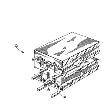
Shown in the various Figures is an edge card connector
10-adapted to couple a mother printed circuit board 12
with a daughter printed circuit board 14 of the edge
card type. Board 14 has contact traces 16 along one
edge 18. A portion of a typical mother prlnted circuit
board is shown in Figure 7 while a typical edge card
type daughter printed circuit board can generally have
two forms. The first form, as shown in Figure 8A, is
also known as the older type of circuit board with
uniform contact strips 16 set at a uniform pitch of
about 100 mils. The second form, as shown in Figure 8B,
is also known as the newer high density type of circuit
board with two different types of contact strips; upper
contact strips 17 and lower contact strips 19. The
upper and iower contact strips 17 and 19 are set at a
uniform pitch of about 50 mils. For the sake of
illustration only, the mother printed circuit board is
shown with apertures 20 at the ends of its electrical
traces for receiving the coupled electrical element such
as the connector of the present invention. Enlarged
apertures 22 and 22a are also included for mechanically
attaching the connector 10 with the board 12. It should
be understood, however, that a surface mount ccnnection
with soldering could be utilized for the coupling
between connector and board. A portion of the daughter
-12-
printed circuit board 14 is illustrated in Figure 8A
with aligned parallel contacts 16 shown. This is that
portion of the daughter board adapted to be releasably
coupled wLth the connector 10 of the instant invention
whereby the individual traces 16 may be coupled with the
individual contacts of the connector for coupling the
mother and daughter printed circuit boards 12 and l~.
The connector 10 is comprised of two basic components,
an electrically nsulating housing ~6 and a plurality of
two types of electrically conductive contacts 28 and 2~.
The contacts function to transmit electrical current,
either signals or power, between the upper edge 30
adjacent to the daughter board and the lower edge 32
adjacent to the mother board. The housing 26 provides
support between the electrical components being coupled
and supports the individual contacts 28 and 29 in the
proper electrically isolated position, with respect to
- each other. The first type of contacts 28 are upper
level contacts intended to be able to make contact with
the contact traces 16 of either the lower type of
circuit board as shown in Fig. 8A or the upper contacts
traces 17 of the high density type of circuit board as
shown in Fig. 8B. In the embodiment shown, the upper
level of contacts 28 are set at a 50 mil pitch with the
second type of contacts 29. The second type of contacts
29 are lower level contacts intended to be able to make
-13-
~qg3S~3~
contact with the lower contact traces 19 of the high
density type of circuit board shown in Fig. 8B, but not
- intended to make contact with the contact traces 16 of
the older type normal density circuit board shown in
Fig. 8A.
The housing 26 is a generally rectangular member molded
of a conventional electrical insulator such as Ryton
R-4, Ryton ~-7, or Ryton R-404. Ryton is a trademark of
the Phillips 66 Company of Pasadena, Texas. The housing
26 is of an extended length 34 largely determined by the
number of contacts to be supported and has a height 36,
through the majority of its extent, slightly less than
the lengths of the supported contacts. Its thickness 38
is relatively ~hin, being merely sufficient to retain
the two rows of opposed contacts with a space 42
therebetween for receiving the daughter board 14 (note
the cross-sectional configuration of Figures 5~ and 5B).
The majority of the bulk of each housing 26 is comprised
of essentially parallel side walls 46 extending the
entire length of the housing and connector. End walls
48, formed integrally at the ends of the side walls,
couple the side walls 46 and are of sufficient thickness
to add rigidity to the housing. One or more
intermediate walls 50 may be spaced periodically along
the length of the side walls parallel with the end walls
for further r~gidity. The side walls 46 and
-14-
3~.3
intermediate walls 50 have upper edges 54 and 56 whilethe daughter printed circuit board 14 has recesses 58
and 60. The asymmetric location of the intermediate
wall 50 and intermediate cutout 58 precludes the
improper locating of the daughter printed circuit board
into the housing. The space 42 is intended to receive
; the edge of the daugh~er printed circuit board 14 and
for this purpose is substantially open with the
exception of portions of the projecting contacts 28 and
29, intermediate walls 50 and keying projections 5L (see
Fig. 5A). In an alternate embodiment of the invention,
the keying projections 51 may be provided as separating
or barrier walls with corresponding slots on the
daughter printed circuit board as described below. The
keying projections 51 are strategically located at a
select and limited number of locations and are intended
to make mating engagement with a keying slot 59 (see
Fig. 8B) in the high density type of circuit boards.
The older type of circuit boards shown in Fig. 8A do not
have a keying slot to accommodate the keying projections
51. Therefore, when an older type of circuit board is
inserted into the connector 10 the keying projections
prevent the leading edge 18 from being inserted into the
lower contacts 29, but merely allows the older type of
circuit board to be inserted and make contact with the
upper contacts 28 and stops the leading edge from
further advancement into the connector 10. This
prevents a relatively wide contact trace 16 on the older
type of circuit board from contacting both an upper and
.
21~5~3~
lower contact 28 and 29, which are relatively close to
each other, thereby preventing cross-over or a short
circuit. Thus~ the high density bi-level connector of
the present invention can be used wlth both the normal
density edge card circuit boards and the high density
edge card circuit boards. Depending projections or
posts 62 and 62a extend downwardly from the intermediate
and end walls for providing a mechanical coupling with
~ the mother circuit board. The posts may be provided
c 10 with different characteristics for proper orientation
with the circuit board. For instance, the diameters of
posts 62 and 62a can be different, as shown in Figure 2,
to provide proper orientation to the circuit board.
Also, the shape of posts 62 and 62a can be different for
15 the same purpose.
A pair of parallel upper bearing strips or shelves 64
extend from end wall to end wall of the housing. Spacer
bars 66 are periodically located between the shelves 64
and their associated side walls 46 to define apertures
20 68 for receiving the upper edge portions of the
individual contacts 28 and 29. The upper interior edges
of the support bars are beveled for guiding the lower
edge of a daughter printed circuit board into the slot.
The lower face of the housing is also provided with a
25 longitudinal support bar 72 and spacer bars 74 defining
-16-
ZC~ 3~
apertures 76 for separating the lower edges of the
individual contacts.
Standoffs 78 are formed into the lower face of the
connector housing to maintain the housing a
predetermined distance from the mother printed circuit
board for functioning as a washway to allow the flow of
fluid therefrom as is necessary durlng the soldering of
the solder tails to the mother printed circuit board.
A vertical central plane 80, shown in Figures 5A and 5B,
separates the connector including the housing and the
rows of contacts into two essentially symmetric halves.
Further, the use of a vertical central plane and the
illustration of an upstanding connector and daughter
printed circuit board in combination with a horizontal
mother circuit board are done for descriptive purposes
only. It should be understood that the present
invention could be practiced at virtually any angular,
planar orientation with respect to the horizontal or
vertical.
Supported within the housing are a plurality of
individual electrical contacts 28 and 29. The contacts
are arranged in two essentially parallel rows 82 and 84
generally symmetric about the vertical central plane 80.
The lower ends 86 and 87 of each opposed pair terminate
in solder tails 88 and 89. In the embodiment shown, the
-17-
2~ 3~
solder tails 88 of the upper contacts 28 are o~fset from
the so1der tails 89 of each adjacent pair of lower
contacts 29. The solder tails 89 are adapted to be
coupled with the electrical traces of the mother printed
circuit board through apertures 20. As shown in Figure
7, the through~hole technique is disclosed herein. It
should be appreciated, however, that surface mount
couplings could just as easily have been utilized.
The solder tails 88 of the upper contacts extend
upwardly into the housing (see Figure 5A) where they
have angled intermediate sections 90 bending toward the
central plane 80 and then outwardly therefrom. At the
area where the terminals bend inwardly then outwardly,
there is a contact area or section 96 constituting a
bight in the connector for making mechanical as well as
electrical contact with the traces 16 of the daughter
printed circuit board 14. Above this region, the
contacts extend upwardly where the uppermost parts 98
are received in their individual apertures 68 defined by
` 20 the side walls 46, shelves 64 and spacer bars 66, as
silown in Figure 3. The individual upper contacts 28 at
their upper ends 94 are constrained from lateral
movement by the spacer bars 66. The spacer bars 66
limit the degree of lateral movement of the upper ends
of the contacts as during the insertion of the daughter
printed circuit board cards into the connector as well
-18-
3~
as during their removal therefrom. The indlvidualcontacts are effectively spring loaded within the
housing against the shelves 64 limiting the movement of
ad]acent contacts of each pair toward each other.
The propes contact stress is thus provided by a
combination of a crown on the contact area with a radius
of curvature similar to that shown in Figure 11 and the
curve on the contact area with a radius of curvature as
seen in Figure-5A, the area where the traces 16 rest
when inserted. The crown is formed by coining and
bending the contact strips in the contact area. The
radius then has a plating placed on it such as a gold.
The crown and the radius jointly provide a combination
of two radii which produce the proper stress when the
contact is placed on the traces 16 of the daughter
- - printed circuit board 14. The gold is used on the
contact primarily for lubricationO
The upper contacts 28 are placed in the housing 26 and
assume a free state. The contacts 28 are then placed in
. . .
their confining apertures 68 as shown in-Figure 5A
whereby they are pre-stressed by hooking behind the
`~ shelves 64. The contacts 28 then are further stressed
when the daughter printed circuit board 14 is inserted
so that their upper ends~94 move off the shelves thereby
placing the proper amount of stress of about 150,000
~ -19-
-
'
35~3B
psi, plus or minus 50,000 psi, on the traces 16 of the
printed circuit board. Tests have shown that the
daughter printed circuit bo~rd may be inserted and
removed a hundred times without degrading performance of
the contact, that is, the contact resistance will not
degrade more than 10 millihoms over the hundred
insertions and removals. When the printed circuit board
14 is inserted, deformation occurs on the upper contact
28 and traces to produce the proper contact. The
modulus of elasticity and the positions ratio are
considered when calculating the proper stress. In this
case, the modulus of elasticity is about 16 million psi
and the poisons ratio is about 0.3.
The solder tails 89 of the lower contacts 29 extend
upwardly into the housing 26 (see Figure 5B) where they
have angled intermediate seceions 91 bending away from
the central plane 80. The contacts 29 bend inwardly and
downwardly back towards the central plane 80 forming a
first bight 200. The first bight 2001 in the embodiment
shown, has a bend of about 158 degrees. However, any
suitable degree of bend could be used. The first bight
generally has a radius of curvature of between about
0.033 to about 0.043 inches. ~s the contacts approach
the central plane 80, they are bent to form a second
25 bight 202 forming a second lower contact area 97 for
making mechanical as well as electrical contact with the
; -20-
~5~)3~
lower traces 19 of the daughter printed circuit board
14~ The contacts 29 then proceed downwardly and have
ends 212 positioned against support bar 72 and are
pre-stressed thereby. However, in an alternate
embodiment of the invention, the ends need not extend
down to the support bar 72. At a second pre-stress area
204 of the lower contacts 29, the contacts 29 are
effectively spring loaded within the housing against
extended shelves 65 limiting the movement of opposing
lower contacts 29 towards each other. The individual
lower contacts are each received in an individual
aperture 6O defined by the side walls 46, shelves 65 and
spacer bars 66. The spacer bars 66 can also constrain
lateral movement of the lower contacts 29.
The proper contact stress fos the lower contacts 29 is
provided by a combination of a crown on the contact area
97 with a radius of curvature as seen in Figure 11 and
the curve on the contact area 97 at the second bight 202
with a radius of curvature as seen in Figure 9, the
contact area 97 being the location where the lower
traces 19 from the new type of daughter printed circuit
boards rest when inserted. The second bight, in the
embodiment shown, generally has a radius of curvature of
between about 0.036 to about 0.040 inches. The crown is
formed by coining and bending the contact strips in the
contact area. The radius then has a plating placed on
-21-
2~ 38
it such as a gold. The crown and the radius jointlyprovide a combination of two radii which produce the
proper stress when the contact is placed on the traces
19 of the daughter printed circuit board 14. The gold
is used on the contact primarily for lubricatlon.
As mentioned above, the lower contacts 29 are
pre-stressed behind the shelves 65 and support bar 72.
The lower contacts are further stressed when a new type
of daughter printed circuit board 14 is inserted so that
the pre-stress area 204 of the contacts 29 move off of
the shelves 65 thereby placing the proper amount of
stress on the lower traces 16 of the daughter printed
circuit board. However, the lower contacts 29 are
provided such that they have a stepped or varied
` 10 application of stress between the contacts 29 and the
lower contact traces 19. As shown in Figure 5B, when
the lower contacts 29 are in a home position with no
daughter printed circuit board inserted into the
connector, the back 210 of the contacts 29 proximate the
first bight 200 are spaced from the side walls 46.
Referrlng now to Figures 12A and 12B, there are shown
schematic views of the daughter printed circuit board 14
being inserted with the lower contacts 29 and into a
final connection position, respectively. As shown in
Figure 12A, when the daughter printed circuit board
makes contact with the contact area 97, the contacts 29
-22-
2~
deflect back Lowards the side walls 46 with the back 210of the contacts proximate the first bight 200 making
contact with the side walls 46. This first deflection
of the contacts 29 has a first spring rate because the
contact is able to deform along substantially all of the
contact above the portion 206 fixedly held in the
housing 26. Once the backs of the contacts 29 contact
the side walls 46 a second deflection occurs with a
second spring rate of the contacts 29. The second
spring rate is greater than the first spring rate
because the contacts 29 can only deform in the area of
the contact between the first and second bights. The
second spring rate comes into effect just before the
leading edge of the daughter printed circuit board 14
passes between the contact portions 97 at the second
15 bights 202. When the daughter printed circuit board 14
is fully lnserted into the connector as shown in Figure
12B, the lower contacts 29 place the proper a~ount of
stress of about 150,000 psi, plus or minus 50,000 psi,
on the lower traces 16 of the printed circuit board.
The dual spring rate of the lower contacts 29 is
generally provided to allow for proper insertion of the
daughter printed circuit board into the connector
without the inserter having to use excess force, but
which nonetheless prevents the circuit board from being
inadvertently removed from the connector and provides a
-23-
2~ 3~
proper electrical contact. Thus, the dual ~step
deflection of the lower contacts is especially desired
in view of the fact that the upper contacts 28 are
already placing a stress of about 150,000 psi on the
printed circuit board even before the leading edge of
the daughter printed circuit board makes contact with
the lower contacts 29.
The cross-sectional configuration of each contact is
essentially rectangular at any point along it5 length
except in the contact zones 96 and 97 where an
electrical contact is made with the traces 16 of the
daughter printed circuit board. In this zone, the
opposed radially exterior faces 102 of each contact
assume a convex configuration (note Figure 11). This
-15 configuration is achieved through coining the contacts
in this region rather than simply stamping them as had
been the custom of the trade. The cross section has
approximately parallel side edges 104 and a
perpendicular radially interior face 106. The bowed
exterior face 102 extends outwardly from the edges 104.
The individual contacts are fabricated of any
conventional spring material such as metal, preferably
phosphor bronze. ~ach contact is plated with nickel to
a thickness of about between 0.000050 and 0.000150
inches. The solder tails are coated with solder of
-24-
03~3
about 60 parts tin and 40 parts lead to a thickness of
about between 0.000100 and 0.000500 inches. In the
contact area, a coating of gold at about 0.000004 inches
nominally is plated over about 0.000040 inches minimum
of about 80 parts palladium and 20 parts nickelO All of
the platings include the plating of all surfaces or
sides except in the contact area wherein the plating
need only occur on that surface to contact the daughter
printed circuit board.
10 The individual contacts are about 0.024 to 0.026 inches
in width 108 being received at the lower part of the
housing in apertures 76 of about 0.033 and 0.034 inches
with the upper apertures 68 being about between 0.028
and 0.032 inchesO The individual contacts are of a
constant rectangular thickness 110 with a maximum total
height 112, a rise of 114 and a radius of curvature 11~.
During the coining process, the width of the strip metal
is increased from about 0.018 to about 0.022 inches.
However, the overall height is generally not changed and
the overall height after coining is essentially or
approximately the same as prior to coining.
The use of a concentrated contact area is desired
because it produces a higher contact stress by reducing
the area which contacts the trace. This stress is
needed to break through any surface film or other debris
-25-
3~
that may be on the pad. The stress required is
` approximately 150,000 psi plus or minus 50,000 psiq
Creating a concentrated contact area in this fashion has
in the past proved to be very difficult to do in a
precisely controlled manner. If a spherical dimple is
put on the contact leg first, then the subsequent
bending of the leg will cause distortion in the contact
area. Such distortion eliminates any control over the
shape of the contact area and places on the surface an
orange peel effect which is not as smooth as required.
On the other hand, if the bend is put in first, then it
is hard to make certain that a spherical dimple ends up
at the intended location. It would thus be difficult to
have the spherical dimple aligned in the center of the
contact. When employing other than the method of the
present invention, the speherical area may be so far out
of center that it interferes with, and breaks through,
the edge of the contact. These problems are amplified
in connectors where the contacts are on the mLniaturized
0.050 center lines as disclosed herein.
The solution to the problem is to place the high stress
configuration on the contact by forming the bend in the
contact and coining during manufacturing, resulting in
the desired compound surface.
The method of fabricating the electrical contact thus
-26-
2~S~313
comprises the steps of initially providlng an elongated
strip of electrically conductive materlal stamped from a
sheet with a lowe} portion and an upper portion. The
strip is then deforrned by coining at an lntermediate
contact area between the lower and upper portions. The
strip is bent at the intermediate contact area to form a
bight with a radially interlor face and a radially
exterior face. The coined area is on the radially
exterior face of the bent strip for contacting a trace
16 of the daughter board to be electrically coupled with
the contact.
Referring to Figures 13 and 14, the method of
fabricating the electrical contacts 28 and 29 and the
bi-level connector 10 will be described. The method of
fabricating the electrical contacts comprises the steps
of initially providing an elongate strip of electrically
conductlve material stamped from a sheet with a lower
portion, an upper portion and intermediate contact
portions. The strip is then deformed by coining the
intermediate contact portions at specific locations on
alternating contact portions. The upper portion is then
removed and the strip is bent at the intermediate
contact portions by a progressive die process to form
the individual upper contacts 28 and lower contacts 29
connected by the lower portion which forms a carry strip
208 provided with both upper and lower contacts 28 and
-27-
2~3~35~3~l
29 in alternating fashion. As shown in ~igure 14, both
the upper and lower contacts can be inserted into a row
of a housing 26 in a single operation and the carry
strip 208 is then simply removed. This single operatlon
S or insertion process saves time and money in the
manufacture of bi-level connectors rather than having to
separately insert lower contacts and then separately
having to insert upper contacts.
The method further includes the step of fabricating the
lQ contacts of phosphor bronze and plating the strip with
nickel to a thickness of about between 0.000050 and
0.000150 inches. The method further includes the step
of plating the lower portion of the contact with solder
of about 60 percent tin and 40 percent lead to a
thickness of about between 0.000100 and 0.000500 inches
to ensure a proper soldering contact with the mother
board. Lastly, the contact area of the contact is
plated with about 40 microinches or thicker PdNi flashed
with gold to a thickness of about 0~000004 inches
nominally. Alternatively, the area can be plated with
about 30 microinches or thicker gold.
The present disclosure includes that information
contained in the appended claims as well as that in the
foregoing description. Although the invention has been
described in its preferred form or embodiment with a
-28-
2~ 5~3~
certain degree of particularity, it i8 understood that
the present disclosure of the preferred form has been
made only by way of example and that numerous changes in
the details of construction, fabrication and use,
including the combination and arrangement of parts, may
be resorted to without departing from the spirit and
scope of the invention.
-29-