Note: Descriptions are shown in the official language in which they were submitted.
The present invention relates to a low noise
amplification microwave integrated circuit (hereinafter MIC)
for use in a satellite broadcasting receiving converter or
microwave communication, and more particularly to an
improvement in an input matching characteristic thereof
Aspects of the prior art and present invention will be
described by reference to the accompanying drawings, in
which:
Fig. 1 is a block diagram of a prior art circuit
~onfiguration,
Fig. 2 is a block diagram of one embodiment of the
present invention, and
Fig. 3 is a Smith chart for a signal source impedance
Zopt and an input reflection coefficient S11* in the
embodiment of Fig. 2.
One o$ prior art low noise ampli$ication MICs uses a
monolithic MIC (hereina~ter MMIC) which uses a ~ield
e$$ect transistor such as a GaAs FET. A general aircuit
coniiguration o$ the MMIC is shown in Fig. 1 in which a
source o$ a FET 21 is grounded, an input matching
- circuit 22 is connected to an input terminal o$ MMIC and
an output matching circuit 23 is connected to an output
terminal o~ MMIC.
In an input matching characteristic of an initial
stage amplifier in a multi-stage amplification MMIC
circuit, either a noise matching characteristic which
requires a low noise characteristic is important or a
gain matching characteristic which requires a high gain
characteristic is important, depending on an application
of the circuit. Constants of elements in the input
15.
; - la -
.
20051~3Z
1 matching circuit 22 are set in accordance with the
characteristic.
In the prior art MMIC, the matching characteristic
of the initial stage amplifier has been designed by
taking primary consideration of only one of the noise
matching characteristic and the gain matching
characteristic, depending on the application. The
circuit designed primarily for the noise matching
characteristic can provide a minimum noise $igure
(hereinafter NF) but a gain of the initial stage
amplifier is low and an input voltage standing wave
ratio (hereinafter VSWR) is high.
In the circuit designed primarily for the gain
matching characteristic, the gain of the initial stage
is high and the input VSWR is low, but the NF is high.
Summar~ of thc Invcntion
Thc prcscnt invcntion intcnds to Eolvc thoEe
problcmG. In the present invention, a microwave
integrated circuit having a plurality of circuit
components integrated therein, comprises an initial
stage ampli$ication means having a $ield effect
transistor and a series circuit means having an
inducti~e element and a variable capacitance element
which are serially connected to each other and one end
o$ the series circuit means is connected to a source of
the field e~fect transistor and the other end being
1 connected to ground.
The present-invention will become more fully under-
stood ~rom the detailed description given hereinbelow
and the accompanying drawings which are given by way of
illustration only, and thus are not to be considered as
limiting the present invention.
Further scope o~ applicability o~ the present inven-
tion will become apparent ~rom the detailed description
given hereina~ter. However, it should be understood
that the detailed description and speci~ic examples,
while indicating pre~erred embodiments of the invention,
are given by way o~ illustration only, since various
changes and modi~ications within the spirit and scope of
the invention will become apparent to those skilled in
the art ~rom this detailed description.
The present invention is now explained in detail
- 3
.
. .
Z00518~
1 with reference to the drawings.
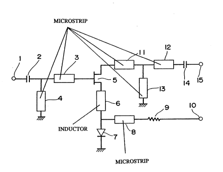
Fig. 2 shows one embodiment of an initial
amplification circuit of MMIC of the present invention.
As shown in Fig. 2, a microwave signal is applied
through a signal input terminal 1 to the initial stage
amplification circuit, a capacitor 2 blocks a DC
component of an input signal, a microstrip 3 is
connected in series to the capacitor 2. An another
microstrip 4 has one end thereof connected to a junction
of the capacitor 2 and the microstrip 3. The
microstrips 3 and 4 form an input matching circuit.
A field effect transistor 5 (hereinafter FET) such
as GaAs MESFET or HEMT has a gate thereof connected to
the microstrip 3. An inductor 6 is constructed by a
microstrip having one end thereof connected to a source
of the FET 5. A variable capacitance diode 7 has an
anode thereof connected to one end of the inductor 6 and
a cathode thereof grounded and a microstrip 8 has one
end thereof connected to a junction of the inductor 6
and the variable capacitance diode 7. A resistor 9 has
one end thereof connected to the other end of the
microstrip 8, and an external terminal 10 is connected
to the other end of the resistor 9.
Microstrips 11 and 12 are connected in series to a
drain of the FET 5, and a microstrip 13 has one end
thereof connected to a junction of the microstrip 11 and
12 and the other end thereof grounded. Those
Z005~82
1 rnicrostrips 11, 12 and 13 constitute an interstage
matching circuit in the multi-stage circuit. A DC
blocking capacitor 14 is connected to the microstrip 12,
and an output terminal 15 is connected to a succeeding
stage circuit.
In the present circuit, a combined impedance Z is
given by
z = j~L ~ l/j~c
= j~(L - 1/~2C) ...~. (1)
where L is an inductance of the inductor 6, and C is a
capacitance of the variable capacitance diode 7.
The constants are selected such that
L > 1/~2C
is met, where W is an operating frequency band, and the
capacitance C of the variable capacitance diode 7 is
changed in accordance with the signal applied to the
external terminal 10 so that the combin0d impedance Z is
changed as a combined inductance Ls.
By changing the combined impedance ~, that is, by
~ changing the combined inductance Ls of the inductance 6
and the variable capacitance diode 7, Zopt (a signal
source impedance which causes a minimum NF) and Sll* (a
complex conjugate number o~ the input re~lection
coefficient) are controlled such that Zopt and Sll*
change on the Smith chart shown in Fig. 3 in a manner
shown by arrows. The reason therefore is explained
blow.
200~;18~
1 The input impedance Zin f the FET5 (which
corresponds to Sl1 in the Smith chart) is given by:
Zin = RG+Rin+Rs+Gm Ls/Cgs+1/(i ~ cgs) --(2)
where RG: gate resistance of the FET 5
Rin:channel resistance
Rs: source resistance
Cgs: gate-source capacitance
Gm: transfer conductance
Zopt is represented by:
Zopt = Ropt + i (Xopt ~/Ls) ..... ( )
where Ropt* real part o~ the signal source impedance
which causes a minimum NF by the FET 5 alone.
XOP~: imaginary part thereof
As seen from the formula (2), the real part of the input
impedance Zin changes in accordance with the combined
impedance Ls. As the combined impedance Ls is increased
by the signal applied to the external terminal 10, the
complex conjugate number S11* of S11 changes as shown by
the arrow on the Smith chart o~ Fig. 3. Namely, it
changes along a constant reactance line in a direction
to increase the resistance.
The imaginary part of the signal source impedance
Zopt changes in accordance with the combined impedance
Ls. As the combined impedance Ls increases, Zopt
changes as shown by the arrow on the Smith chart.
Namely, it changes along a constant resistance circle in
a direction to reduce the reactance.
Z00518Z
1 Accordingly, by properly selecting the combined
impedance LS(Z) by the input signal applied to the
external 10, S11* and Zopt approach to each other on the
Smith chart so that the trade-o~ between the noise
matching characteristic and the gain matching
characteristic is optimized.
While the initial stage ampli~ication circuit o~ the
~ MMIC has been described in the present embodiment, the
present invention is applicable to a multi-stage
ampli~ication type MMIC in which a plurality o~ the
initial stage ampli~ication circuits are connected in
series.
While the MMIC has been described in the present
embodiment, the present in~ention is also applicable to
a hybrid MIC and a discrete component circuit with a
similar advantage.
. ~: ' -. ' .. . ~ , '.... . . .
' ' ' '
.
.
: . ..
`, , :