Note: Descriptions are shown in the official language in which they were submitted.
2005528
- 1 - 20LC01535
POWER CONVERSION SYSTEM INCLUDING AN
Ih~KO~ FILTER FOR A. ~NuATING HARMONICS
Background of the Invention
This invention relates to an electric power
conversion system for conveying power between a direct
current (d-c) power source and an electric load circuit,
and, more particularly, it relates to a system of this
type that includes a controllable converter and an
improved electrical filter for partially isolating the
converter from source transients and for attenuating
harmonics developed by the system in operation.
Electric power conversion systems are used to
condition the electric power supplied to motor load
circuits from a d-c source of relatively constant
voltage. If supplying d-c motors, such a system will
include an electric power "chopper" that is suitably
controlled to vary the magnitude of load current and/or
voltage as desired. Alternatively, in the case of
alternating current (a-c) motors, the system will
include an electric power "inverter" that is suitably
controlled to vary the amplitude and frequency of load
voltage as desired. In either case, electric power
flows from the d-c source terminals to the load
terminals of the controllable converter during
"motoring~' operation or in a reverse direction during
"electrical braking".
200S5~8
- 2 - 20LC01535
Such a system is useful for propelling a rapid
transit vehicle, in which case the source comprises a
wayside conductor and the load comprises windings of at
least one traction motor whose rotatable shaft is
mechanically coupled through torque-increasing gearing
to an axle-wheel set of the vehicle. The wayside
conductor is typically energized by a relatively low
voltage d-c power generating plant located near the
right of way along which the vehicle travels. In its
motoring or propulsion mode of operation, the converter
is so controlled that the d-c voltage applied to its
source terminals is converted into adjustable voltage at
its load terminals, and the traction motor(s) responds
by producing torque to accelerate the vehicle or
maintain its speed as desired.
In the alternative electrical braking or
retarding mode of operation of the power conversion
system, the converter is so controlled that each motor
acts as a generator driven by the inertia of the vehicle
and supplies electric power which flows in a reverse
direction through the converter and appears as direct
current and unipolarity voltage at the source terminals.
As this electrical energy is used or dissipated, the
traction motor(s) responds by absorbing kinetic energy
and slowing the vehicle. Electrical braking is achieved
by a combination of dynamic braking and regenerative
braking. Dynamic braking is effected by connecting a
dynamic braking resistance between the d-c source
terminals. This resistance receives current from the
converter, converts the electrical energy to thermal
energy, and dissipates the resulting heat. Regenerative
braking, on the other hand, is effected by returning to
the d-c power source power flowing in a reverse
direction through the converter during braking
operation. These two electrical braking modes can be
200552~3
-
- 3 - 20LC01535
combined in desired proportions, this mixing process
being commonly referred to as "blending".
A power conversion system including a voltage
source inverter for supplying a-c tracti;on motors is
disclosed in U.S. Patent 3,890,551, Plunkett, issued
June 17, 1975 and assigned to the assignee of the
present invention. An important feature of the Plunkett
power conversion system is its inclusion of ohmic
resistance (shown at 28 in FIG. 1 of the Plunkett
patent) that is inserted into the d-c link between the
inverter and the d-c power source during electrical
braking but is effectively removed from the d-c link
during motoring. By inserting this series resistor
during electrical braking, the magnitude of voltage at
the d-c terminals of the inverter can increase above
that of the source voltage. One of the advantages of
thus raising the inverter voltage is to enable the
traction motors to develop more magnetic flux for
braking and to use less current than would otherwise be
required for very high braking effort.
The power conversion system of the Plunkett
patent also includes a low pass electrical filter of the
conventional series inductance (L), shunt capacitance
(C) type between the voltage raising resistor and the
inverter for attenuating harmonics generated by
operation of the inverter and for partially isolating
the inverter from undesirable line transients. (As used
herein, the term "harmonics" refers to various
components of the composite current and voltage
waveforms having frequencies that are multiples of the
frequency of the fundamental component of such
waveforms). In addition, the shunt capacitance of the
filter at the d-c terminals of the inverter provides the
"stiff" voltage required for proper operation of a
voltage source inverter.
Z00.~528
- 4 - 20LC01535
The desired blending of dynamic and
regenerative braking can be accomplished in various
different ways that are well known to persons skilled in
the art. See, for example, U.S. Patent 4,093,900,~
Plunkett, issued June 6, 1978. In the present state-of-
the-art it is preferable to replace the parallel array
of separate braking resistors and their respectively
associated electromechanical switches, as shown in the
aforementioned U.S. Patent 4,093,900, with a single bank
of resistance elements connected to the d-c link via an
electric power chopper comprising a controllable solid-
state electric valve that can be repetitively turned on
and off in a pulse width modulation (PWM) mode to
control the average magnitude of current in the resistor
as desired. An example of this modern practice is
disclosed in U.S. Patent 4,761,600, D'Atre et al, issued
August 2, 1988, where the electric valve comprises a
main thyristor or silicon controlled rectifier (SCR) and
an auxiliary thyristor for commutating the main SCR from
a conducting state (on) to a non-conducting or current
blocking state (off). Alternatively, a solid-state gate
turn-off device (GT0) could be substituted for the
chopper shown in the aforementioned U.S. Patent
4,761,600.
Summary of the Invention
A general objective of the present invention
is to provide, in an electric power conversion system of
the general type disclosed by Plunkett, a filter wherein
the required inductance and capacitance means are
interconnected and arranged in an improved and
synergistic manner that saves space, weight and costs
and/or that enhances reliability.
Another objective is to provide an improved
filter capable of fulfilling the immediately-preceding
objective and of enabling the voltage raising resistor
200~5Z~3
_
- 5 - 20LC01535
that is inserted in the d-c link to provide beneficial
damping to the filter transfer function that is in
effect when the power conversion system is operating in
the electrical braking mode.
Still another object is to provide a
relatively compact and low cost filter capable not only
of effectively attenuating harmonics generated by
converter operation but also capable of effectively
attenuating harmonics generated by operation of a
chopper that controls the current flowing through the
above-mentioned dynamic braking resistance during
electrical braking.
In carrying out the invention in one form, a
set of load terminals on the motor side of a
controllable converter is adapted to be connected to at
least one electric motor, and means is provided for
connecting a pair of source terminals of the converter
to a d-c power source via an electrical filter that
attenuates harmonics generated during motoring and
electrical braking operation of the converter. The
filter comprises: (1) line-filter inductance means
connected in the current path between the d-c source and
the converter, (2) first capacitance means directly
connected between the source terminals of the converter,
(3) second capacitance means, and (4) interconnecting
means characterized by the absence of appreciable
inductance for connecting the second capacitance means
in parallel with the first capacitance means. A dynamic
braking circuit is connected across the second
capacitance means and comprises the series combination
of a dynamic braking resistance and an electrical power
chopper that can be repetitively turned on and off
during electrical braking to control current in such
resistance. The interconnecting means of the aforesaid
filter includes additional ohmic resistance means in the
Z005~8
- 6 - 20LC01535
path of current between said two capacitance means so
that during electrical braking a substantially higher
voltage is developed across the first capacitance means
than across said second capacitance means. This
additional resistance means is effectively removed from
the interconnecting means during motoring operation.
The capacitance value of the second capacitance means is
selected to attenuate harmonics generated by operation
of the chopper during electrical braking.
For a better understanding of the invention,
reference may be had to the following detailed
description taken in conjunction with the accompanying
drawings.
Brief Description of the Drawings
FIG. 1 is a schematic circuit diagram of one
embodiment of the invention; and
FIG. 2 is a schematic circuit diagram of
another embodiment of the invention.
Detailed Description
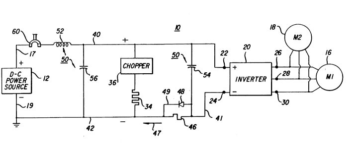
Referring now to FIG. 1, there is shown a
power conversion system 10 for conveying power between a
d-c power source 12 and an electric load comprising
first and second motors 16 and 18 electrically connected
in parallel. In one application of the invention, the
motors 16 and 18 are three-phase a-c induction-type
traction motors used for propelling a transit vehicle
(not shown), and the d-c source 12 comprises a wayside
power distribution system including either a third rail
or an overhead catenary with which a current collected
on the vehicle makes sliding or rolling contact. In
FIG. 1, the relatively positive line 17 represents such
a current collector, and the negative line 19 represents
a conductor in contact with a grounded rail serving as
the other terminal of the d-c source. Alternatively,
the power conversion system lo on board the vehicle may
Z~0~28
- 7 - 20LC01535
be connected to the source via a two-wire trolley in
contact with two parallel conductors of an overhead
catenary. The magnitude of the unipolarity voltage
between the lines 17 and 19 is typically in a range from
600 volts normal to 800 volts maximum, and each of the
motors 16 and 18 typically has a full-load rating on the
order of 300 horsepower more or less.
The power conversion system 10 includes a
controllable converter 20 which, in the illustrated
embodiment of the invention, is a voltage source
inverter having a pair of d-c terminals 22 and 24 on its
source side and a set of three a-c terminals 26, 28 and
30 on its motor side. The d-c terminal 22 is connected
via a conductor 40 to the line 17 of positive potential,
and the terminal 24 is connected via relatively negative
conductors 41 and 42 to the other line 19 of the d-c
power source 12. The conductors 40-42 thus serve as a
d-c link between the source 12 and the inverter 20. The
a-c terminals 26, 28 and 30 are respectively connected
to the three different phases of each of the a-c motors
16 and 18.
During motoring, i.e. when electrical power is
being conveyed from the source to the motors, direct
current is supplied to the inverter through its d-c
terminals 22 and 24, and the inverter acts to convert
this direct current into alternating current supplied
through a-c terminals 26, 28 and 38 to the two motors 16
and 18. The inverter is of a conventional design and
includes suitable controls (not shown in FIG. 1) for
varying the amplitude and frequency of the alternating
voltage at its a-c terminals to provide the needed
acceleration or deceleration of the vehicle driven by
the motors 16, 18. The well known pulse-width modulated
(PWM) control strategy can be used. Examples of useful
inverters are disclosed in the aforementioned U.S.
2~0~
- 8 - 20LC01535
Patents 3,890,551 and 4,761,600. In modern practice,
GTO devices are preferred as the main controllable
electrical valves of the inverter, thereby avoiding the
need for auxiliary thyristors and commutation circuits.
The power conversion system 10 has alternative motoring
and electrical braking modes of operation. During
electrical braking, each of the motors 16 and 18
operates as an electrical generator driven by the
inertia of the transit vehicle, returning power to the
system 10. This return power flows through the inverter
20 in a reverse direction from the direction of flow
during motoring and appears as unipolarity voltage and
direct current at the d-c terminals 22 and 24.
The conversion system 10 is designed to
provide for both dynamic braking and regenerative
braking. Dynamic braking is effected by connecting
across the conductors 40 and 42 of the d-c link a
dynamic braking resistance 34 through which at least
some of the braking current can be made to flow, thus
dissipating electric energy in the form of heat. For
controlling current in the resistance 34 an electric
power chopper 36 is connected in series therewith. As
is well known to persons skilled in the art, the chopper
36 is a solid-state switch that can be repetitively
turned on and off by suitable control means (not shown
in FIG. 1) that, in one form, controls the ratio of the
"on time" to the "off time" during successive intervals
each of fixed duration. The average magnitude of
current in the resistance varies-directly with this
ratio.
Regenerative braking is effected by returning
reversely-flowing power to the d-c source 12. During
this mode of braking, braking current from the d-c
terminals 22 and 24 flows through the source 12 via the
d-c link conductors 40, 41 and 42. Regenerated power
20~528
-
- 9 - 20LC01535
can be used for propelling other vehicles connected to
the wayside conductor and then drawing power from the
same source. But, as noted in the aforementioned U.S.
Patent 4,093,900, there are many instances when a power
source is not receptive enough to use all of the
electrical braking energy, and in such instances some
energy must be dissipated in the dynamic braking
resistance 34. The chopper control is able to sense
such conditions and to respond by varying the on-off
ratio of the chopper appropriately. One approach for
controlling electrical braking is to use only the
regenerative braking mode as long as the resulting
braking effort is sufficient but to blend in dynamic
braking effort when regenerative braking effort drops
below the desired level.
For increasing the effectiveness of the
braking action, additional ohmic resistance means 46 is
connected between the two negative conductors 41 on one
side of the d-c link so that it is in the path of
current flowing from the relatively negative line 19 of
the d-c power source 12 and/or the dynamic braking
circuit 34, 36 to the negative d-c terminal 24 of the
inverter during electrical braking. This resistance
means 46 is shunted by a bypass circuit 49 including
suitable means 48, such as the illustrated diode, for
effectively removing the resistor 46 from the d-c link
- during motoring (i.e. when current in the conductors 41
and 42 flows in the direction of arrow 47 from the
negative d-c terminal 24 of the inverter 20 to the
negative line 19 of the source 12). The diode 48 in the
bypass circuit 49 is poled, as is shown in FIG. 1, to
present negligible resistance to current in the
direction of the arrow 47, but during electrical braking
it blocks current which now flows in an opposite
direction through conductors 41 and 42, thereby forcing
;~00~5Z8
-
- 10 - 20LC01535
such current to flow through the resistor 46.into the
path of braking current, the voltage developed between
the d-c terminals 22 and 24 of the inverter will have a
substantially higher magnitude than the voltage between
conductors 40 and 42 of the d-c link. Consequently, the
amplitude of the motor voltage will rise above the
magnitude of source voltage when the motors are acting
as generators during electrical braking.
Such increased voltage is highly advantageous
because it enables the motors to develop more flux for
braking, and very high braking effort can be obtained
with less current than would otherwise be possible. In
a typical transit vehicle, the peak braking power will
be much higher than the maximum power for propulsion.
Keeping the maximum current as low as possible during
braking has the additional benefit of avoiding the need
for larger diameter and more expensive solid-state
electrical valves in the inverter 20. This action and
its other advantages are explained in more detail in the
previously referenced U.S. Patent 3,890,551. It is
apparent that the extra resistor 46 will always absorb a
portion of the electrical braking power even when the
source 12 is highly receptive and there is no current in
the dynamic braking circuit 34, 36. During regenerative
braking the resistor 46 provides an additional benefit:
it partially isolates the inverter 20 from the voltage
between the lines 17 and 19, which voltage may
experience wide magnitude swings in either a positive or
negative direction for many milliseconds due to
lightning strokes, opening and closing of line breakers,
or the like. The presence of the resistor 46 gives the
inverter control circuits some additional time to
respond to these sudden transients in a safe and
controlled manner.
For attenuating harmonics generated by
2005528
- 11 - 20LC01535
operation of the power conversion system 10 and for
effectively isolating the system from any undesirable
electrical transients in the d-c power source 12, a
single-stage electrical filter 50 of the L-C type is
included in the connections between the source 12 and
the inverter 20. This filter 50 comprises a series
line-filter inductance means 52 connected in the path of
current between the line 17 and the positive conductor
40 of the d-c link, and shunt capacitance means 54, 56.
In accordance with the present invention, the shunt
capacitance means actually comprises two separate,
parallel banks of capacitors. The first capacitance
means 54 (referred to as the d-c link capacitor) spans
the conductors 40 and 41 and thus is directly connected
between the two d-c terminals 22 and 24 of the inverter.
The second capacitance means 56 (referred to as the line
capacitor) spans the conductors 40 and 42 and thus is
interconnected in parallel with the capacitance means 54
via a circuit that includes the additional resistor 46
and its bypass circuit 49. During motoring, the bypass
circuit around the resistor 46 is in its low resistance
state as described above, essentially the same voltage
is applied across both of the capacitors 54 and 56, and
the effective value of capacitance in the filter 50 is
the sum of the capacitance values of the capacitors 54
and 56. But during electrical braking (when braking
current is flowing in a direction opposite to the arrow
47), the resistor 46 is inserted in the path of braking
current between the line capacitor 56 and the d-c link
capacitor 54, and the voltage magnitude across the
former capacitor will now be less than the voltage
across the capacitor 54 by an amount equal to the
voltage drop across resistor 46.
In either mode of operation, the filter 50
serves to attenuate harmonics generated by operation
200~SZ~
- 12 - 2OLC01535
of the inverter 20 so that such harmonics are isolated
from the d-c source 12 and will not interfere with the
usual wayside signaling system. During motoring, the
d-c link capacitor 54 serves mainly as the required
"stiff" voltage source for the inverter 20. In the
electrical braking mode of operation, the line capacitor
56 serves mainly as a filter for the chopper 36,
providing a temporary path for braking current during
the off periods of the chopper in the dynamic braking
circuit 34, 36 which, as can be seen in FIG. 1, is
connected across this capacitor. In addition to
attenuating chopper-generated harmonics, the filter 50
cooperates with the resistor 46 to damp the
inverter-generated harmonics during electrical braking.
An important advantage of inserting the
resistor 46 between the two capacitors 54 and 56 during
electrical braking is that its presence enables the
voltage between the inverter terminals 22 and 24 to rise
to a desired high magnitude during this interval without
subjecting the line capacitor 56 to this elevated
voltage. As a result, only the d-c link capacitor 54
needs to have the capacity of sustaining this higher
voltage. The line capacitor 56 has a significantly
lower voltage rating, whereby it is smaller, less
expensive and more reliable than would be true if the
higher voltage rating were required. In one application
of this circuit, the magnitude of voltage at the d-c
terminals 22, 24 can rise to a maximum of about 1200
volts during electrical braking, whereas the maximum
voltage across capacitor 56 is only about 800 volts.
With the resistor 46 being connected between the
negative d-c terminal 24 of the inverter 20 and the
negative line 19 of the source 12, the potential on the
terminal 24 during electrical braking is negative
relative to ground by an amount equal to the voltage
ZOOS5Z~3
-
- 13 - 20LC01535
drop across the resistor 46, and the positive potential
on the other inverter terminal 22 will rise above ground
by an amount equal to, but not more than, the magnitude
of source voltage, whereby the benefits of increased
motor voltage during braking are obtained without the
detriment of excessive electrical stress on the
insulation systems of the motors 16 and 18.
In accordance with the present invention, the
means for interconnecting the parallel capacitors 54 and
56 of the single-stage L-C filter 50 has no appreciable
inductance. To this end, no inductor or reactor is
deliberately or intentionally inserted between these two
capacitors. Of course, there is a small amount of
distributed inductance due to the layout of the cables
or bus bars that interconnect the two capacitors and the
additional resistor 46 and diode 48, but such inherent
inductance has insufficient value (less than
approximately five microhenrys) to appreciably smooth
the undulating current in the d-c link 40-42. Stated
another way, the inductance in the interconnecting means
is less than the value of inductance required
effectively to attenuate the ripple amplitude or
harmonics in the d-c link current. Limiting the
inductance to a low value minimizes circulating currents
between the two capacitors by keeping circuit resonance
well above any ambient disturbance frequency. While
substantially higher inductance in the interconnecting
means could keep the circuit resonance well below such
disturbance frequency and therefore would also serve to
inhibit undesirable circulating currents, it would add
undesirable weight, size and cost.
In the presently preferred embodiment of the
invention, the line capacitor 56 has a substantially
higher capacitance value than the d-c link capacitor 54.
For example, the line capacitor 56 could typically have
20055Z8
- 14 - 20LC01535
a value of about 58,000 microfarads as compared to a
value of less than about 9,000 microfarads for capacitor
54, or many times more capacitance. A typical
inductance value for the line-filter inductance means 52
of the L-C filter 50 is about 400 microhenrys, and a
typical ohmic value of the additional resistor 46 is
about 0.75 ohm.
In a practical embodiment of the invention,
the line capacitor 56 actually comprises a bank of 40
individual capacitor units (or cans) arranged in 20
parallel branches, each branch containing two units in
series, with each unit having a capacitance value of
about 5,800 microfarads, a voltage rating of 450 volts,
and a current rating of 18 amps r.m.s. The d-c link
capacitor 54 actually comprises a bank of 24 capacitor
units (or cans) arranged in six parallel branches, each
branch containing four units in series, with each of
these units having a capacitance value of about 5,800
microfarads, a voltage rating of 450 volts, and a
current rating of 18 amps r.m.s.
Although the capacitance bank forming the
second capacitance means 56 has a much higher
capacitance value than the capacitor bank forming the
first capacitance means 54, it uses only one-fourth the
number of capacitance units as would be required if it
had to withstand the same maximum voltage as the first
capacitor bank (54). This is due to the resistor 46
inserted between the two capacitor banks during
electrical braking, whereby the magnitude of voltage
across the second capacitor bank (56) will not exceed
the level of source voltage between lines 17 and 19 even
though the magnitude of voltage at the d-c terminals 22,
24 of the inverter 20 is higher. In addition, the
resistor 46 is believed to cooperate with the two
capacitors 54 and 56 to provide beneficial damping to
Z0055;~8
-
- 15 - 20LC01535
the filter transfer function in effect during electrical
braking. This should make the system inherently easier
to stabilize with little increase in complexity or
component cost.
For disconnecting the power conversion system
10, an electric circuit breaker 60, applied in a
conventional manner, is provided between the system and
the d-c power source. This circuit breaker 60 is
operated from its closed position shown to an open
position in response to a fault or whenever the system
10 needs to be isolated from the source 12.
In a typical transit vehicle, there will be a
second voltage source inverter, in addition to the
inverter shown in FIG. 1, for supplying alternating
current to two more traction motors for propelling the
vehicle. FIG. 2 illustrates a power conversion system
including such an additional inverter and with third and
fourth a-c motors being connected to the set of the a-c
terminals on its motor side. In FIG. 2, components
common to those shown in FIG. 1 and described above are
designated by the same reference numerals used in FIG.
1, and corresponding added components are designated by
the same reference numerals plus the suffix "a".
Referring now to FIG. 2, the positive d-c
terminal 22a on the source side of the second inverter
20a is connected, via the conductor 40 of the d-c link,
to the line 17 of positive potential, and the relatively
negative d-c terminal 24a is connected, via a separate
conductor 4la and the common conductor 42, to the other
line 19 of the d-c power source 12. The a-c terminals
26a, 28a and 30a of the inverter 20a are respectively
connected to three different phases of each of the a-c
motors 16a and 18a. A second d-c link capacitor 54a
individually associated with the inverter 20a is
directly connected between the d-c terminals 22a and
2005~28
- 16 - 20LC01535
24a, and a line capacitor 56 shared by both of the
inverters 20 and 2Oa and both of the choppers 36 and 36a
spans the conductors 40 and 42 of the d-c link where it
is effectively in parallel circuit relationship with the
two d-c link capacitors 54 and 54a during the motoring
mode of operation of the FIG. 2 conversion system.
As is shown in FIG. 2, a second dynamic
braking circuit, comprising the series combination of
another dynamic braking resistor 34a and a second
electric power chopper 36a, is connected between the d-c
link conductors 40 and 42 and hence across the line
capacitor 56. A second additional ohmic resistance
means 46a bypassed by a diode 48a is connected in the
path of current between the capacitors 54a and 56. The
diode 48a is poled to conduct d-c link current during
motoring, thereby effectively short circuiting the
resistor 46a. But it blocks current during electrical
braking so that the resistor 46a is then inserted in the
braking current path and causes a substantially higher
voltage to develop across the d-c link capacitor 54a
than across the line capacitor 56. As before, the
current path between the capacitors 54a and 56 is
characterized by the absence of appreciable inductance.
In addition to sharing the common shunt line
capacitor 56, the two inverters 20 and 20a utilize the
same series line-filter inductance means 62 which is
connected on the d-c power source side of the capacitor
56 between the d-c link conductor 40 and the line 17.
The line-filter inductance means 62 in FIG. 2 has the
same inductance value as the line-filter inductor 52 of
the FIG. 1 embodiment, but its current rating is higher.
The two inverters 20 and 20a are controlled
from a common control means 70 which responds to
alternative command signals from interlocked throttle
and brake controllers 72 and 74, respectively. The
20C)5~28
-
- 17 - 20LC01535
control means 70 also receives feedback signals
representative of sensed values of voltage, current, and
other selected variables in each of the inverters 20 and
2Oa. To operate in a dynamic braking mode, the control
means 70 derives a train of suitably timed periodic
signals that determine the repetitive on and off
intervals of the choppers 36 and 36a, and it varies the
ratio of these intervals as desired. This signal train
is fed over a line 76 to the first chopper 36 and also
to suitable means 77 for splitting it into a separate
train of periodic signals that are displaced from the
signals of the original train on the line 76 by a length
of time corresponding to approximately one-half the
period of such signals. The separate signal train is
fed over a line 78 to the second chopper 36a. In this
manner the two choppers are coordinated so as to operate
alternately rather than in unison. That is, the "on"
periods of chopper 36a are staggered in time with
respect to the "on" periods of chopper 36. This
staggering reduces the amplitude and increases the
frequency of the braking current traversing the line
capacitor 56, thereby making it much easier for this
capacitor, which is then acting as a filter for
attenuating the harmonics generated by operation of both
of the choppers, to perform its filtering function.
In the FIG. 1 embodiment, where there are two
motors and one chopper, the dominant frequency of the
current through the line capacitor 56 during dynamic
braking is the same as the fundamental operating
frequency of the chopper 36 (e.g. 200 Hz). But in the
FIG. 2 embodiment, where the total magnitude of braking
current is doubled but two choppers are operating in a
staggered relationship, the line capacitor 56 sees only
half the total current at a doubled frequency, and thus
it can more effectively perform its desired function.
;~005S2~3
- 18 - 20LC01535
As a result, the capacitance value of the common line
capacitor 56 in FIG. 2 can be the same as that of the
capacitor 56 in FIG. 1 to perform the required filtering
action.
In the FIG. 2 embodiment, the individual
series resistance means 46 and 46a serve an additional
beneficial function. They help to isolate or buffer the
inverters 20 and 20a from each other, particularly
during electrical braking, thus reducing the risk of
undesirable interference between the two inverters, a
condition which might otherwise be caused by the
charging of the common line filter capacitor 56.
The above-described embodiments of the
invention are illustrative only, and various changes and
modifications can be made without departing from the
invention in its broader aspects. One such change is
that the additional resistor 46 and its bypass circuit
49 can be located in the relatively positive d-c link
conductor 40 between the capacitors 54 and 56 instead of
being associated with the negative sides of these
capacitors as is shown in FIG. 1. Additional changes
and modifications will be apparent to those skilled in
the art, and the concluding claims are therefore
intended to cover all such changes and modifications as
fall within the true spirit and scope of the invention.