Note: Descriptions are shown in the official language in which they were submitted.
PROGRAMMABLE OPTION SELECTION AND PAGED
- MEMORY CACHE COHERENCY CONTRO~
:
The invention relates to memory control systems used
in computer systems, and more particularly to systems
utilizing cache memory and paged main memory.
.
~` Personal computer systems are becoming increasingly
prevalent and increasingly more powerful. Early personal
computer system~, while a great advance over manual
; 10 systems, were relatively simple and had limited
capabilities. Personal computers took a step forward in
capabilities when International Business Machines
Corporation (IBM) introduced the original IB~ PC. That
computer was based on the 8088 microprocessor developed by
15 Intel Corporation. The IBM PC was more powerful than :`
earlier personal computers and new functions and
capabilities for the IBM PC were rapidly developed. The
components available for use in personal computers
advanced significantly over this period and soon the
design of the IBM PC was too limited, especially after the
.
:
- --2--
}S~
- introduction by Intel Corporation of the 80286
microprocessor.
Personal computer users were d~manding the available
improvements and IBM introduced the IBM PC/AT, which
utilized the ~0~86 microprocessor and many of the advanced
devices which had been developed since the IBM PC was
introduced. This machine satisfied users for a period of
time, but again the capabilities of available components
for use in personal computers increased and ~he demand for
increased performance persisted.
The operating system utilized in IBM compatible
: computers was developed for use with the IBM PC and its
incorporated 8088 microprocessor. The 8088 has 20 address
pins and so only 1 Mbyte of memory is directly
addressable. This was satisfactory in ~he early stages,
but ~he availability of the 80286 and its 24 address lines
and the need for progxams accessing more than the
available 640 kbytes of random access memory under the
operating system rendered the operating system a
limitation on personal computer performance. Various
formats were developed to resolve this operating system
limitation. One such format was the LIM expanded memory
specification (LIM EMS), which used a window available in
the memory space accessible under the operating system to
access more memory. The location of the window over the
physically available memory was controlled by information
passed through the input/output space. Thus,
significantly greater amounts of memory could be accessed
without a revision of the operating system and with only
the inclusion of window control programming in the
application program utilizing the additional memory.
To abate the usex demand, Intel Corp. introduced the
80386 microprocessor. The increased speed of this unit
helped to temporarily resolve the performance demand
problem, but soon users still demanded more performance.
One technique used in advanced or large computer
architectures to increase performance was ~he use of cache
'
. .
'
. .. .
5~3 ~
memory. Cache memory is very fast memory which allows the
microprocessor to operate at its full potential when
operating out of this fast memory, unlike when op~rating
out of main memory, where cost considerations limit the
~ speed of the memory utilized. However, because of the
relatively high cost of this cache memory, only portions
of the information in the main memory are kept in the
cache memory. This use of only portions requires that the
cache memory system keep track of which portions of the
main memory are duplicated in the cache memory.
This requirement to keep track of which portions of
the main memory are located in the cache memory, called
- coherency, is difficult when utilizing memories which
- implement the LIM EMS or other paged memory technigues,
wherein different physical memory locations can be
addressed at the same logical address. For example, if
the LIM EMS window is pointing to a first physical memory
location and the cache memory saves the data at this
location, the cache memory system thinks it h~s stored the
data at a given location in the logical address space of
the window. The window is then moved to a different
! physical portion of the memory, but ~he window logical
address does not change. Thus the information present at
the location preserved by the cache memory system is not
what is currently present at that location. This creates
a cache coherency problem and the specific location in the
cache memory must be cleared or nullified.
One device commonly utilized in present personal
computer systems to control the cache memory is the Intel
Corporation 82385 cache controller. The 82385 does not
allow individual cache memory locations to be cleared
under certain circumstances, such as those described
above. To this end, a cache flush operation must be
performed which clears all entries in the cache memory
i~ 35 system. In the past, to avoid the difficulties of
determining when a cache flush was necessary, the designs
have required that the applications programs or drivers
' ` ' . ` ' .~ .
'',, ` ' ~ ' : `
-4-
9B
used with LIM or paged memory systems insure that
coherency problems did not develop. This was a burden on
the programs and reduced their performance.
With the user demand for higher performance noted, a
number of sources considered the architecture o~ the AT
insufficient to properly utilize the full capabilities of
then available components and of components which would
clearly be available in the relatively near future.
Certain operations, such as multiple bus master
operations, were exceedingly difficult to perform and only
marginal performance improvements could be obtained. To
~- this end a new architecture or interface standard was
developed.
IBM introduced a new line of personal computers,
called the Personal System/2 or PS/2. A number of the
machines available in the PS/2 family utilized the new
interface standard, referred to as the Nicro Channel
Architecture or MCA, to allow the advanced, desired
capabilities to be provided at a high performance level.
In addition to the conventional address, data and control
signals necessary for operation, the MCA provides a card
selected feedback signal or CD SFDBK*(n), where the (n~
indicates that a separate signal exists for each circuit
board location. This signal provides feedback to the
computer system to indicate which circuit board has
responded to the operation presented on the system signal
bus. For detailed information on the MCA, please refer to
the IBM Personal System/2 Model 80 Technical Reference
Manual, having a copyright date of l9B7 and a product
number of 84X1508.
One of the features provided by the MCA was the
ability to initialize circuit board parhmeters entirely by
program control, without the need to set any jumpers or
switches. This feature was called Progr~mmable Option
Select ~POS) and utilized certain defined input/output
~I/O) space locations or ports to control which circuit
boards or adaptors were being configur~d a~d where
- . . . - ~
6 9 ~
configuration information was to be located. A circuit
board was configured by first selecting which circuit
board location was to be addressed and placing the circuit
board in setup or configuration mode. The configuration
information was then loaded and setup mode exited.
Configuration information which could be transferred
depended on the function of the particular circuit board
being configured. For example, if a memory board w~s
being configured, the information would include the memory
space address locations to which the memory board would
respond.
This programmable configuration capability is
desirable, but also creates a potential cache coherency
problem, similar to ~hose discussed previously. The cache
memory system could remember a gi~en logical address and
the computer system could reconfigure its resources, with
another element ending up at the given logical address.
Additionally, reconfiguration is a high level function
which indicates major changes could be occurring in the
computer system, with many possible cache coherency
ramifications.
A computer system utilizing the MCA standard and an
82385 cache controller and incorporating the present
invention determines when circuit boards are being
configured or when an installed circui~ board responds to
an input/output space write operation and then issues a
cache flush reguest. The request can be disabled on a
circuit board location by circuit board location basis.
The system monitors write operations to the Adapter
Enable/Setup register defined in the MCA and decodes which
circuit board is being configured. The decoded signal is
combined with a signal from a register which contains
information on which circuit board locations have the
cache flush option enabled. These signals are also
X~05~8
combined with system signals which indicate that an
input/output space write operation is occurring.
A second portion of the system monitors the card
selected feedback signals and combines these signals with
S the location enabled signals and the input/output space
write operation signals.
If either operation is occurring and that location is
enabled, a cache flush signal is transmitted to the cache
flush input on the 82385 cache controller.
The system also provides circuitry for directly
requesting a cache flush to occur by sensing when a
particular bit in a particular input/output space or port
;l is written, to allow additional flexibility in design and
implementation of the various programs that c~n be
operated on the computer system.
A better understanding of ~he invention can be
obtained when the following detailed description of the
preferred embodiment is considered in conjunction with the
following drawings, in which:
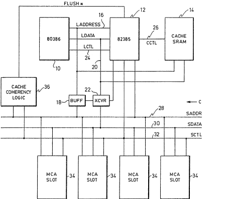
; Figure 1 is a block diagram of a computer system
: incorporating the present invention;
Figure 2 is a diagram indicating the relative
relationships between Figures 2A, 2B and 2C; and
Figures 2A, 2B and 2C are schematic diagrams of
electrical circuitry for requesting a cache flush
operation according to the present invention; Figure 2C appears
with Figure 1.
,
Referring now to Figure 1, the letter C generally ~-
refers to a computer system incorporating the present
invention. The computer includes an Intel Corporation
80386 microprocessor 10, an Intel Corporation 82385 cache
controller 12 and a series of static random access
memories (SRAM's) forming a cache memory unit 14. A local
35 address bus 16 is connected ~etween th~ 80386 10, ~he
82385 12, the cache RAM 14 and a buffer 18. A local data
,. . . ; .
.. .
~- -7-
~ 8
bus 20 is co~nected to the 80386 10, the 82385 12 and the
cache RAM 14 as well as a transceiver 22. A local control
bus 24 is connected between the 80386 10 and the 82385 12.
~ cache control bus 26 connects the 82385 12 and the cache
SRAM 14 to provide proper control of the cache SRAM 14 as
appropriate.
The buffer 18 and transceiver 22 are used to
interface the local busses to the system busses which form
portions of the Micro Channel Architecture. This local
bus arrangement allows the microprocessor to operate at
faster speeds and to allow concurrent opexations during
certain intervals and opera~ions. The buffer 18 is
connected between the local address bus 16 and the system
address bus ~8. The transceiver 22 is connected between
the local data bus 20 and the system data bus 30. The
system control bus is connected to the 82385 12 and is
driven by the 82385 12, as explained in more detail in
publications relating to the operation and description of
~he 82385, such as pages 4-287 to 4-348 of the October
1987 Volume I of the Microprocessor and Peripheral
Handbook published by Intel Corporation.
The various MCA slots or locations are shown as MCA
slots 34 and are connected to the ~ystem address bus 28,
the system data bus 30 and the system control bus 32.
This allows the various slots 34 to receive and transmit
the necessary informatiQn to allow proper operation of any
circuit boards included in the slots. Additionally,
connected to the system address bus 28 and the system
control bus 32 is the cache coherency logic 36, which
contains the circuitry of the present invention utilized
in determining the state of the FLUSH* signal provided to
the flush input of the 82385 12. The cache coherency
logic 36 is more fully disclosed in Figs. 2, 2A, 2B and
2C.
As previously mentioned, cache coherency problems can
result when a circuit board is being reconfigured or when
the paging or memory locatisn of ~he LIM E~S window, for
,
.
., , . . , . . -
,, .. - . .. , ., j .
` example/ are changed. In the computer according to the
present invention, this occurs only during input/output
~I/O) write operations. Therefore, it is necessary to
determine when valid I/O operations are occurring. In the
5 MCA, this condition is established or indicated by the S1*
signal being high, the S0* signal being low and the M-IO*
signal being low. To this end, ~he S0* signal, the M-IO*
signal and the inverted S1* ~ignal are provided to the
": inputs of a status latch 50. The gating signal for this
10 status latch 50 is the ADL* signal which is used for
` address and status value latching. The use of the status
latch 50 allows the I/O write information to be retained
for the proper intervals. The outputs from the status
~; latch 50 are connected to three of the six inputs of an OR .
15 gate 52 in a channel activity module 54. Eight identical
modules 54 are utilized in the preferred embodiment, with
only one module 54 shown in Fig. 2A in detail for reasons
.~` of clarity. Additionally connected to one input of the OR
gate 52 is the CMD* signal, which is used by the MCA to
20 indicate that state of the data present on the system data
. bus 30. Therefore, the combination of the latched Sl*
inverted signal, the latched S0* signal and the latched
' M-I9* signal, in addition to the CMD* signal provide an
indication, when all ~he signals are low, that an I/O
25 write operation is occurring and the data is valid.
It is also necessary to determine which slot or card
locations have been activated to allow cache flushing
~ based upon these I/O write operations. This information
r is stored in a slot enabled latch 56. The inputs to the
30 slot enabled latch 56 are connected to the D<7:0~ si~nals
of the data lines which are contained in the system d~ta
bus 30. The slot enabled latch 56 is gated by a signal
referred to as CWRT104*. This is a signal which indicates
; that the I/O operation is a write operation occurring to
35 address 104 and that the system of ~he preferred
embodiment is in a special mode which allows access to
- this latch 56. In the MCA, the I/O port locations 100-107
~ -, - . ~ ~ . . .....
have given and defined functions. In some cas~s the
amount of storage space available at these l~cations this
may be determined to be insufficient, and therefore an
alternate method has been determined to access additional
information and register storing capability and yet remain
within these allowed port locations. Each output line of
the slot enabled latch 56 is connected to a channel
activity module 54. The specific signal or output line is
connected to an inverter 58, whose output is then
connected to one input o~ the OR gate 52. Thus, if a
given bit or location in the slot enabled latch 56 is set
to a high condition, that particùlar slot or location is
enabled for flush operation request, while if it is set to
a low condition, the inverted value of a one or high level
appearing at the OR gate 52 is such that a high signal
always appears on the output of OR gate 52, thus disabling
operation of that particular location's cache flush
request capability.
A slot enabled buffer 60 (Fig. 2B) has its input
connected to the outputs of the latch 56 and its output
connected to the D<7:~> lines to provide the feedback to
the computer system so that the value contained in the
slot enabled latch 56 can be read. The gating signal
which enables the output of the slot enabled buffer 60 is
a signal referred to as CRD104*, which is the complement
to the CWRT104* signal, so that when a read request is
issued to I/O port 104 and the machine is operating in the
special mode, the values of the slot enabled latch 56 are
read.
It is now necessary to determine whether a given slot
or location is in configuration mode or whether a card in
that slot has responded to the current operation. Because
of the specified characteristics of the MCA, even though
- - . . . .. . . ...
,. , . ...... ~ . . :
,. .::: . ~ . - .. ,
-10-
2~
board configuration is done by writing to the I/O space,
the SFDBK* signal which is normally utilized to indicate
that a board is responding to current operation, is not
- utilized during configuration mode and therefore separate
circuitry must be utilized to determine this case. I/O
port 96 is defined as the port for accessing the channel
- or board position select register ~not shown). The three
least significant bits of the position select register are
utilized to indicate which of the various circuit boards
is to be configured, with the next more significant bit
indicating that board configuration is in operation.
- These four bits are provided to a configuration latch 62,
with the gating signal tc the configuration latch 62 being
a signal referred to as WRT96*, which indicates that a
write operation is occurring to I/O port address 96.
; The three least significant bits, bits 0, 1 and 2 of
' the D<7-0> signals, are latched and provided to the three
selection inputs of a 3-8 decoder 64. The fourth bit,
referred to as bit 3, is provided to the positi~ enable
bit of the decoder 64. The decoder 64 also has two low
true enable inputs. These inputs are connected to the
- output of an AND gate 66 whose two inputs are the SPOSIO*
` and CPOSIO* signals. These signals indicate a standard
IBM compatible mode POS I/O operation is occurring or a
special mode POS I/O operation is occurring, respectively,
when the signal is low. The outputs of the 3-8 decoder 64
are low true outputs of a line referring to the binary
value selected at the three selection inputs. The 8
output lines of the decoder 64 are connected to the
channel activity module~ 54, one line to each module 54.
The output line of the decoder 64 is connected to one
input of an AND gate 68. The output of the AND gate 68 is
the fin~l input to OR gate 52. Thus, if a given board
location is enabled for configuration, the appropriate
output of the decoder 64 is low, so that a low value is
provided to the input of the OR gate ~. If that
particular board location is not being configured, a high
,.. , . : - .. . . .
` ' --ll--
2~ 56~3
value will be provided to the input of the AND gate 68
and, if thie othier input to the AND gate 68 is high, then a
high value is applied to the OR gate 52 and that specific
board location would not trigger a cache flush operation.
The second input to the AND gate 68 contained in each
of the channel act}vity modules 54 i~ provided b~ the
output of a feedback latch 70, whose inputs are connected
to the 8 CD_SFDBK* signals. These signals, as specified
in the MCA, are used to indicate that a given circuit
board in thiat given slot or location has responded to thie
current operation, in this case an I/O write operation.
Thus it is not necessary to provide address decoding
- capabilities which understand which I/O locations are
being used by circuit boards. It is merely necessary to
monitor the CD SFDBR* lines and to determine if boards are
being configured to determine if a cache flush operation
is necessary. The gating signal to the fee~back latch 70
is provided by the ADL* signal and corresponds to tbie
timing indicated in the MCA specifications. Therefore,
the inputs to the AND gate 68 are generally in a high
state unless that particular board is responding to an
operation or is being configured, and ~herefore the OR
gate 52 is generally producing a high output. The output
of the OR gate 52 is low only during the C~D* portion of
an I/O write operation, when the particular channel is
enabled and configuration mode is entered or an operation
response is occurring.
The outputs of the 8 channel activity modules 54 are
8 inputs to a 9 input flush AND gate 72 ~Fig. 2C). The
output of this flush AND gate 72 is the FLUSH* signal.
The ninth input to the flush AND gate 72 is connected to
circuitry which allows a cache flush operation to be
reguested directly by the microprocessor. A selected bit,
in this case bit 2 of the data line, is present as one
input to a three input NAND gate 74. The second input to
this three input NAND gate 74 is a signal referred to as
CPOS105, which indicates that an I/O operation is
-12-
~ ~ ~ S6 ~ ~
occurring to port 105 during system board co~figuratlon in
the special mode. This combination is used to trigger the
actuation of the cache flush. The third input to the NAND
gate 74 is the output of an AND gate 76, which AND gatP
output is also the input to the flush AND gate 72. The
output of the N~ND gate 74 is provided as one input of an
OR gate 78, with the second input of the OR gate 78 being
the CMD* signal. In this manner, the state of the NAND
gate 74 is only passed through the OR gate 78 during the
active portion of the CMD* signal. The output of the OR
gate 78 is connected to one input of the AND gate 76. The
CMD* signal is also connected to one input of a second OR
gate 80, whose second input is connected to the output of
the AND gate 76. The output of the OR gate 80 is the
second input to the AND gate 76. This feeaback path from
the AND gate 76 to the OR gate 80 and the ~AND gate 74 is
used so ~hat the output puls2 from the AND 76 is only the
length of the CMD* signal and no greater. When the signal
from the AND gate 76 goes low, this terminates the active
state of the output signal from ~he ~AND gate 74, causing
it to go high. However, this signal from the NAND gate 74
has also been propagated through the OR gate 80 as a low
signal, so that the input to the AND gate 76 from OR gate
80 is still low and thu~ the feedback situation continues
until the CMD* signal goes high, at which time, after the
propagation delays o the various gates, the output signal
of the AND ~ate 76 goes high, ending ~he cache flush
request.
The FLUS~* signal is held low for a time sufficient
to allow the 82385 12 to fully flush or clear the tag
valid bits. The FLUSH* signal is low for a ~ufficient
time when developed as indicated because the length of the
CMD* signal during ~n I/O write operation is sufficient to
insure that the 82385 12 has received at least eight CLK2
cycles. Thus, no extra circuitry is necessary. However,
such circuitry could be added between th~ flush AND gate
,, , " , ,
72 and the 82385 12 if n~eces ~ y to insure the minimum
time.
Therefore, the circuits described above cause a cache
flush operation to occur whenever a slot or location is in
configuration mode or a circuit board is responding to the
current bus operation, that particular location is enabled
and an I/O write operation is occurring. This insures
cache coherency should the circuit board be a memory board
or other board and the memory space location are changed.
The foregoing disclosure and description of the
invention are illustrative and explanatory thereof, and
various changes in the size, shape, materials, components,
circuitry, wiring connections and contacts, as well as in
the details of the illustrated circuitry, construction and
- 15 method of operation may be made without departing from the
spirit of the invention.
, .
.. -. - . ~ . . . ..