Note: Descriptions are shown in the official language in which they were submitted.
;;~OOS~729
TITLE OF THE INVENTION
Method and Apparatus for Forming Electrode on
Electronic Component
- BACXGROUND OF THE INVENTION
Field of the Invention
The present invention relates to a method and an
apparatus for forming an electrode on a part of an end
surface, for example, of an electronic component with
: electrode paste, and more particularly, it relates to a
method and an apparatus for applying electrode paste to a
portion of an electronic component to be provided with an
. electrode.
Description of the Background Art
Referring to Fig. 9, electrodes 2 are ormed on
prescribed outer surface regions of an electronic
component 1. Each electrode 2 serially extends over an
end surface la of the electronic component 1 and
respective ones of-an opposite pair of major surfaces lb
and lc, which are in series with the end surface la
through opposite edges of the end surface la. Thus, the
electrode 2 has a U-shaped section as a whole, and
comprises an electrode part 2a which is positioned on the
end surface la and electrode parts 2b and 2c which are
positioned on the major surfaces lb and lc respectively.
~. ' . .
!. .
.. ~ .
;' .
~ ~ .
;~0057Z9
In general, such electrodes 2 are typically formed by
one of the following two methods employing screen
printing:
Fig. 10 shows the first method, in which electronic
components 1 are received in cavities 11, which are
provided in a hclder 10, so that upper end surfaces la
thereof upwardly pro~ect from the cavities 11. Screen
printing is performed from above the projecting upper end
surfaces la to form electrode parts 2a. Then, another
holder 12 having caYities 13 is prepared as shown in Fig.
11, to receive the electronic components 1 in the cavities
13 in a sidelong manner as shown in Fig. 12. In this
state, screen printing is performed on first major
surfaces lb of the electronic components 1, which are in
series with the end surfaces la, to form electrode parts
2b. Then, the electronic components 1 are so turned over
in the cavities 13 as to upwardly direct second major
surfaces lc, and screen printing is performed to form
electrode parts 2c.
Fig. 13 shows the second method, in which electronic
components 1 are upwardly arranged between a pair of clamp
members 15. Similarly to the first method, screen
printing is performed on end surfaces la of the electronic
components 1 to form electrode parts 2a. Then the
aforementioned holder 12 is employed to separately perform
;~0057;~9
screen printing on major surfaces lb and lc of the
electronic components 1, thereby forming electrode parts
2b and 2c respectively.
In the first and second methods, the electrode parts
2a are formed by screen printing in different manners,
while the electrode parts 2b and 2c are formed in the same
step.
According to the first method, however, as shown in
Fig. 14, parts of electrode paste 2d may be adhered to
upper edge portions of a pair of walls defining each
cavity 11 during screen printing of each electrode part
2a. Such electrode paste 2d may enter the cavity 11
through a clearance defined around the electronic
component 1 which is received therein, to stain the
electronic component 1. Further, a screen employed for
screen printing is pressed by irregular surfaces of the
electronic components 1 projecting from the upper openings
of the cavities 11 as shown in Fig. 10, and hence the
screen is expanded or damaged.
In the second method, on the other hand, electrode
paste may cause a capillary phenomenon to enter clearances
between the electronic components 1, which are arranged in
close contact with each other so that the end surfaces la
thereof are subjected to screen printing. Thus, the
electronic components 1 may be stained by the electrode
-- 3 --
.,' .
:~j
r.;
;~005'729
paste. In order to pre~ent this, it is necessary to
interpose spacers 14 of paper or the like between the
electronic components 1, as shown in Fig. 15. However, it
takes time to interpose the spacers 14 between the
electronic components 1. Also in the second method, the
screen for printing is expanded or damaged similarly to
the first method.
In addition, the first and second methods commonly
have the following disadvantages:
If an end surface la of an electronic component 1 to
be screen-printed is rounded as shown in Fig. 16, printed
electrode paste 2e is irregularized in thickness over the
center and end portions along the direction of thickness
of the electronic component 1.
Fuxther, the electrode parts 2a, 2b and 2c of the
electrodes 2 must be formed in different steps
respectively. In order to carry out these steps, it is
necessary to transfer the electronic components 1 from the
holder 10 or the clamp member 15 to the holder 12 and to
turn over the same within the holder 12, while drying
steps are required after the steps of printing the
electrode parts 2a, 2b and 2c respectively. Thus, the
operation for printing the electrodes 2 is extremely
inefficient.
- .
: - ' '
;~0~15~7~9
Each electrode 2 i8 ~ormed by separately printing the
three electrode parts 2a, 2b and 2c, and hence the
electrode part 2a may deviate from the electrode part 2b
and/or the electrode part 2c (not shown), as shown in Fig.
17. Such deviation will be further promoted if the screen
is expanded or damaged-as-hereinabove described, for
example. The screen may be also expanded or damaged when
the same is used over a long period of time.
The electrode paste is exposed to the outside air
during the screen printing steps. Thus, viscosity of the
paste may be undesirably changed by evaporation of a
solvent contained therein. Such change in viscosity of
the paste results in change in thickness of a printed
paste film. Thus, the printed paste film may be changed
in thickness with time during screen printing.
SUMMARY OF THE INVENTION
Accordingly, an object of the present invention is to
provide a method and an apparatus for forming an electrode
on an electronic component, which can solve the
aforementioned problems caused by screen printing.
In the inventive method of forming electrodes on an
electronic component, first prepared are a slit plate
which is provided with a through slit having width
corresponding to the width of an electrode to be formed,
and a bath of electrode paste for forming an electrode.
~t~ : -
.,' .
.. ~
. ~ .
2005'7Z9
The slit plate is located above the electrode paste bath.
An electronic component is arranged above the slit plate
so that a surface of the electronic component to be
provided with an electrode extends across the through a
S slit. ~efore or after this step, the electrode paste bath
is brought to a level reaching the surface to be provided
with an electrode through the through slit. Thus, the
electrode paste passes through the through slit and is
applied to the surface to be provided with an electrode.
In the step of bringing the electrode paste bath to a
level reaching the surface to be pro~ided with an
electrode, the electrode paste may be made to partially
upwardly swell beyond the upper surface of the slit plate,
so that an electrode can be simultaneously formed to
extend over an end surface of the electronic component as
well as opposite major surfaces which are in series with
the end surface.
` The inventive method is preferably carried out with
; an apparatus having the following structure: This
apparatus comprises a container having an opening upper
surface for storing electrode paste for forming an
electrode. The aforementioned slit plate is arranged to
close the upper surface of the container. This apparatus
further comprises means for providing pressure condition
causing such pressure difference that the pressure within
. ' .
,,
;~00S'7;~9
the container is higher than that in the exterior of the
container, thereby raising up the electrode paste in the
through slit.
According to the present invention, the electrode
paste is brought to a level reaching the surface to be
provided with an electrode through the through slit, to be
adhered to the electronic component. Thus, it is possible
to simultaneously form an electrode on the end surface of
the electronic component and the two major surfaces which
are in series with the end surface by making the electrode
paste swell beyond the upper surface of the slit plate, if
necessary. Further, it is also possible to form an
electrode substantially in uniform thickness even if the
end surface of the electronic component is rounded.
According to the present invention, the problems
caused by expansion or damage of the screen for screen
printing can be solved since no screen printing is
employed. Thus, the electrode can be formed in high
dimensional accuracy. For example, it is possible to form
electrodes which are narrower than those formed by screen
printing, by reducing the width of the through slit and
increasing viscosity of the electrode paste.
It is possible to substantially seal the electrode
paste by storing the electrode paste in a container and
arranging the slit plate to close an opening of the
. . ,
,
;~0()57X9
container. Thus, the electrode paste can be prevented
from time change of viscosity since a solvent etc.
contained therein hardly evaporates. Consequently, it i8
possible to reduce time change in thickn~ss of the
electrode paste.
These and other objects, features, aspects and
advantages of the present invention will become more
apparent from the following detailed description of the
present invention when taken in conjunction with the
accompanying drawings.
BRIEF DESCRIPTION OF THE DRAWINGS
Fig. 1 is a longitudinal sectional view showing an
- electrode forming apparatus according to an embodiment of
the present invention;
Figs. 2, 3 and 4 show steps carried out for forming
electrodes through the electrode forming apparatus shown
in Fig. 1;
Fig. 5 is a perspective view showing a part of an
electronic component 1 which is provided with electrodes
through the steps shown in Figs. 2, 3 and 4;
Fig. 6 is a perspective view showing a step of
scraping off parts of electrode paste remaining on the
upper surface of a slit plate;
.. -
20()57;~9
Fig. 7 is a longitudinal sectional view showing an
electrode forming apparatus according to another
embodiment of the present invention;
Fig. ~ is a sectional view showing the structure of a
slit plate employed in still another embodiment of the
present invention;
Fig. 9 is a perspective view showing a part of an
electronic component which is formed with electrodes by a
conventional method;
Fig. 10 is a perspective view showing a holder
employed in a first conventional method of forming
electrodes and electronic components held by the holder;
Fig. 11 is a perspective view showing another holder
employed in a step carried out after the step shown in
lS Fig. 10;
Fig. 12 is a sectional view of the holder shown in
Fig. 11, with electronic components being received in
cavitles;
- Fig. 13 is a front elevational view showing a step
carried out in a second conventional method of forming
electrodes;
Fig. 14 is an enlarged sectional view showing a part
of the holder shown in Fig. 10, for illustrating a problem
caused in the first conventional method;
_ g _
.. .
~.
~, . . . . .
~005~9
Fig. 15 is a front elevational view for illustrating
a method which is employable for solving a problem caused
in the second conventional method;
Fig. 16 is an enlarged sectional view showing a part
of an electronic component for illustrating a problem
commonly caused in the first and second conventional
methods; and
Fig. 17 is a perspective view showing a part of an
electronic component for illustrating another problem
commonly caused in the first and second conventional
methods.
DESCRIPTION OF THE PREFERRED EMBODIMENTS
Fig. 1 shows an electrode forming apparatus according
to an embodiment of the present invention.
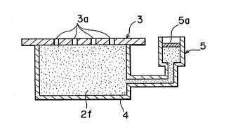
This apparatus comprises a slit plate 3 having
through slits 3a which are provided in prescribed width at
regular intervals in correspondence to the number and
positions of electrodes to be formed on electronic
components, a container 4 storing electrode paste 2f so
that the slit pLate 3 is placed thereon, and pressure
means 5 provided on the lateral side of the container 4.
A presser plate 5a, which is provided on the pressure
means 5, is pushed down to press the electrode paste 2f,
thereby extruding parts of the electrode paste 2f through
the through slits 3a. The junction between the slit plate
-- 10 --
;, .
. . .
. .
: . .
;~OOS'729
3 and the container 4 is so seal~d as to prevent lea~age
of the electrode paste 2~.
When a prescribed preparation step of bringing the
electrode paste 2f to a prescribed temperature or the like
is completed, an electronic component 1 is upwardly held
by a holding member (not shown) or the li~e and placed on
the slit plate 3 so that an end surface la of the
electronic component 1 to be provided with electrodes
extends across the through slits 3a, as shown in Fig. 2.
The slit plate 3 and the electronic component 1 may define
a clearance therebetween, or may be in contact with each
; other.
Then the pressure means 5 is driven to extrude a
desired volume of the electrode paste 2f from the through
slits 3a provided in the slit plate 3, as shown in Fig. 3.
Thus, parts of the electrode paste 2f swell from the slit
plate 3, to be adhered to the end surface la of the
electronic component 1 and two major surfaces lb and lc
whlch are in series with the end surface la.
Thereafter parts of the electrode paste 2f left on
the slit plate 3 are returned to the container 4, and the
electronic component 1 is lifted up as shown in Fig. 4.
Thus, strip-shaped electrodes 2 having ~-shaped sections
are simultaneously formed on the electronic component 1 in
a single electrode forming process over the end surface la
. .
~.
,: ~
~ . ,
~. .
.:
. .
~ .
;~0(~5'7~9
and the major surfaces lb and lc, as shown in Fig. 5. The
electronic component l may be lifted up before the parts
of the electrode paste 2f are returned to the container 4.
Then, parts of the electrode paste 2f adhered to the
upper surface of the slit plate 3 are scraped off with a
scraper 6 which is in the form of a triangle pole, for
example, as shown-in Fig. 6. This step is not necessary
if no electrode paste 2f is adhered to the upper surface
of the slit plate 3. It is noted that parts of the
electrode paste 2f remaining in the through slits 3a will
not stain the electronic component 1.
Thereafter the above electrode forming process is
performed on a next electronic component.
Although the electronic component l is first placed
on the slit plate 3 and the electrode paste 2f is
thereafter extruded on the slit plate 3 in this
embodiment, it is also possible to first upwardly extrude
the electrode paste 2f to a constant level from the slit
plate 3 and thereafter place the electronic component 1 on
the slit plate 3, thereby forming the electrodes 2.
While the pressure means 5 is provided on the lateral
side of the container 4 to upwardly extrude the electrode
paste 2f from the slit plate 3 in the above embodiment,
the present invention is not restricted to this. For
example, the container 4 may be introduced into a vacuum
.. . . .
'''" ' , '
:
;~0()5'7~9
cham~er 7 as shown in Fig. 7 to couple the side surface of
the container 4 with a pipe 8 which has an end provided on
the exterior of the chamber 7 and decompress the interior
of the chamber 7 through vacuum suction by a vacuum pump
(not shown) or the like as shown by an arrow 16, thereby
sucking up the electrode paste 2f through the slit plate 3
as shown by arrows 17.
Alternatively, it is also possible to mount side
plates 9 around the slit plate 3 to provide upper ends
which extend beyond the upper sur~ace of the slit plate 3
~i- as shown in Fig. 8, and submerge the slit plate 3 in an
electrode paste bath within such a range that the level of
; the electrode paste bath is not higher than the upper ends
of the side plates 9. Then the electrode paste is made to
.~?
swell to a constant level from the through slits 3a,
thereby forming electrodes on an electronic component.
Although the electronic component 1 is directly
placed on the slit plate 3 in the aforementioned
embodiment, the present invention is not restricted to
this. For example, an elastic sheet may be adhered to the
upper surface of the slit plate 3, to improve contact of
the slit plate 3 with the electronic component 1. Thus,
it is possible to suppress spreading of the electrode
paste which is adhered to the electronic component during
:,
- 13 -
.j:,: .
...
... .
;~00~'7;~9
application, thereby preventing the slit plate 3 from
; staining.
According to the present invention, a large number of
electronic components 1 may be arranged on the slit plate
~ 5 3 to form electrodes, in order to enable multiple
;; processing.
In the aforementioned embodiment, the electronic
: component l has a flat end surface la and an opposite pair
of major surfaces lb and lc which are in series with the
end surface la through opposite edges of the end surface
i la, while the electrodes 2 are formed to extend over the
first and second edges of the end surface la toward parts
of the major surfaces lb and lc, as shown in Fig. 5.
However, the present invention is also applicable to the
case of forming electrodes only on the end surface la, as
well as the case of foxming electrodes on the end surfacP
la and one of the major surfaces lb and lc.
Fuxther, the present invention can also be applied to
the case of forming electrodes on the rounded end surface
la of the electronic component l as shown in Fig. 16, for
example.
Although the present invention has been described and
illustrated in detail, it is clearly understood that the
same is by way of illustration and example only and is not
to be taken by way of limitation, the scope of the present
- 14 -
~j
~,. .
~: .
;~005'~29
invention being limited only by the terms of the apponded
claims.
, !
)
~ - 15 -
:
' . .
, .,; . .
~,
. ,: .