Note: Descriptions are shown in the official language in which they were submitted.
~006050
VISUAL DISPLAY DEVICE WITH FLUORESCENT -~
DYE-DOPED EDGE-ILLUMINATING EMITTER PANEL
BACKGROUND OF THE INVENTION
Field of the Invention
The present invention generally relates to visual
display panels, and more specifically to a novel and unique
combination of a fluorescent dye-doped edge-illuminating
emitter panel with such a visual display panel.
Description of the Related Art
Visual display panels such as liquid crystal displays
(LCD), direct view dashboard displays, virtual image
displays, aviation heads-up displays (HUD) on partial
reflectors or holographs and automotive center-high-mounted
stop light displays are becoming increasing popular in many
applications in varied technical fields. In combination -
with the development of these display panels comes an
increasing requirement to reduce their profile both in sizie
and the visibility of the light source and other elements
which do not form the actual display pattern. Further, it
is desirable to reduce the power requirements for the
display pane]. illumination sources.
In particular, red colored, center-high-mounted stop-
j light devices (CHMSL) for automotive vehicles are becoming
increasingly popular due to the increased safety margin
they provide. In addition to the conventional right and
left mounted, red-colored rear braXe lights, newer vehicles
and retrofit packages for older vehicles are available
which include the center-high-mounted stoplight device in
~ '`.
.
,
Z~060S0
the form of a third brake light which is mounted near the
top of the vehicle rear window. Depression of the vehicle
brake pedal causes the center-high-mounted stoplight device
to be illuminated in combination with the two low mounted
brake lights to form a triangle pattern with enhanced
visibility and ability to attract the attention of the
operator of a trailing vehicle. Experience indicates that
the center-high-mounted stoplight devices have prevented
traffic accidents in situations requiring emergency braking
under high speed, congested traffic conditions.
Existing center-high-mounted stoplight devices general-
ly an opaque housing with a rear-facing translucent red
panel, and with an illuminating bulb inside the housing
wired to the vehicle's brake circuit. The opaque housing
itself constitutes a safety hazard in that it blocks a
portion of the view out the rear window which the vehicle
operator must see via the rear-view mirror. An opaque
housing, or at least a light blocking member behind the
illuminating bulb and red panel, is necessary to prevent
the vehicle operator from confusing the center-high-mounted
stoplight display with a light from a trailing vehicle.
Another category of display is the liquid crystal
display (LCD), which has become popular in clocks and other
analog and digital readout applications. These are essen-
tially passive devices which require external illumination.Liquid crystal displays are generally transparent panels
with imbedded segment or other patterns formed from a
I material which is normally transparent in the absence of an
applied electric field, and which becomes opaque upon
application of an electric field, or vice-versa. A liquid
crystal display may be utilized in a transmission mode with
illumination from the rear, or in a reflection mode with
illumination from t~he front. Both modes are highly affect-
ed by ambient light which swamps the generally weak applied
illumination, resulting in low visibility and contrast.
~: :
. ~
~` '`
~3 ~
:
200~0
SUMMARY OF THE INVENTION
In accordance with the present invention, the
drawbacks of the related art are overcome by combining a
light emitting or illuminating panel with a display panel,
and edge coupling light from the emitter panel into the
display panel in coordination with the indices of
refraction and total internal reflection angles of the
panels. The light emitting panel is formed from a
transparent plastic substrate doped with a fluorescent dye
which absorbs incident light through a relatively large
surface area and emits light of a longer wavelength through
the edges. The incident light may be either ambient or
produced by a fluorescent light source. The edge emitted
light is optically coupled into an edge of a display panel,
which may be a polymer dispersed liquid crystal display or
a plastic panel having a display surface formed with an
etched or printed pattern, grating or hologram.
The substrate materials of the emitting and display
panels, as well as an optical adhesive which joins the
edges thereof, preferably have an essentially similar index
of refraction which is larger than that of air. Light
propagating through the panels is thus internally
reflected, and exits the structure only through the pattern
on the display surface. The display panel is preferably
transparent in the absence of light incident on the
emitting panel, and produces a display visible from only
one direction upon application of incident light. The
display panel may be a center-high-mounted stop light for
an automotive vehicle.
It is a purpose of an aspect of the present invention
to provide an automotive center-high-mounted stop light,
polymer dispersed liquid crystal, or holographic visual
display device with a fluorescent dye-doped edge-
illuminating emitter panel which combines the component
elements thereof in a novel and heretofore unknown manner.
A purpose of an aspect of the present invention is to
provide a visual display device which may preferably be
. '~
~ .
o
configured as a center-high-mounted stoplight having a
display panel which is transparent in both directions in
the absence of illuminating light. Upon illumination of an
associated linear edge coupling emitter panel, the display
panel remains transparent in one direction and provides a
high intensity visual output in the opposite direction.
A purpose of an aspect of the present invention is to
provide a visual display device which is capable of
operating either with or without the addition of an
~0 auxiliary light source, and which is self-regulating in
intensity in response to the ambient light level.
A purpose of an aspect of the present invention is to
provide a visual display device which is simple in
structure, employing a luminescence plastic sheet as an
emitter panel and a visual display or light output coupling
panel on the same substrate or host material as the emitter
panel. The two component panels are attached together
using an optical adhesive which has the same index of
refraction as the plastic sheets, thus ensuring maximum
transmission at their interface. No extra optical
components are needed to achieve high coupling efficiency
between the linear light source and visual output coupler.
A purpose of an aspect of the present invention is to
provide a high efficiency visual display device which uses
a commercially available green fluorescent lamp as a
preferred light pumping source, and a red edge-emitting
sheet for center-high-mounted stoplight applications.
Other purposes of aspects of the invention are to
provide a visual display device which may be fabricated at
low cost on a commercial production basis from readily
I available materials which is capable of providing a multi-color display, and has a substantially reduced profile
achieved by relocating an illumination source from the
front or rear of the device to an unobtrusive edge coupling
~ 35 location.
3j Other aspects of this invention are as follows:
i A visual display device, comprising:
. .
! l
20050~0
4a
display panel means formed with a display pattern on
a surface thereof and having a light receiving edge; and
fluorescent dye doped emitter panel means for
absorbing light incident upon a surface thereof and
emitting light through an edge thereof, said edges of said
emitter and display panel means being optically coupled to
each other for edge illumination of said display pattern,
said emitter and display panel means each comprising light
transmitting substrates.
A stoplight device for an automotive vehicle,
comprising:
fluorescent dye doped emitter panel means for
absorbing light incident upon a surface thereof and
emitting light through an edge thereof;
light source means for radiating light onto said
surface of the emitter panel means in response to
application of a vehicle brake; and
display panel means formed with a stoplight display
pattern on a surface thereof and having an edge which is
optically coupled to said edge of the emitter panel means
for edge illumination of the display pattern.
A liquid crystal display device, comprising:
fluorescent dye doped emitter panel means for
absorbing light incident upon a surface thereof and5 emitting light through an edge thereof; and
liquid crystal display panel means having a display
pattern on a surface thereof and having an edge which is
optically coupled to said edge of the emitter panel means
for edge illumination of the display pattern.
' ~:~
. ,~ ~,
; , '~
Z(~()605i0
: 5 .-
: ::
These and other features and advantages of the present
invention will be apparent to those skilled in the art from
the following detailed description of several preferred :. :
embodiments, taken together with the ~ccompanying drawings, ~ .
in which like reference numerals refer to like parts. ~
~ .: :
DESCRIPTION OF ~HE DRAWINGS
FIG. 1 is a diagram illustrating the optical properties
of fluorescent dye-doped polymer films;
FIGs. 2a and 2b are graphs illustrating the absorption
and emission spectral characteristics respectively of
fluorescent dye-doped polymer films;
FIG. 3 is an elevational view of a generic embodiment
of a visual display device in the form of an automotive
center-high-mounted stop light, polymer dispersed liquid
crystal (PDLC), or holographic or similar visual display
device with a fluorescent dye-doped edge-illuminating
emitter panel embodying the present invention;
E`IG. 4 is a sectional view of an embodiment of a visual
display device in accordance with the present invention
comprising a display panel in the fGrm of a PDLC display;
FIG. 5 is a sectional view of a modified PDLC display
panel for use in the present invention;
FIG. 6 is an elevational view of a visual display
device in accordance with the present invention comprising
a display panel having a pattern ln the form of engraved
grooves;
FIG. 7 is a fragmentary sectional view of a visual
display device in acordance with the present invention
comprising a display panel having a pattern formed by
printed ink;
FIG. 8 is a fragmentary sectional view of a visual
display device in accordance with the present invention
comprising a display panel having a pattern formed as an
optical diffraction grating; and
~ ~,
,
2005060
FIGs. g and 10 are elevational views of alternative
embodiments of emitter panels in accordance with the
present invention.
DETAILED DESCRIPTION OF THE INVENTION
The present invention employs a fluorescent dye-doped
polymer film or sheet to edge-couple light into a display
panel. FIG. 1 of the drawings illustrates the properties
of an acrylic or polycarbonate polymer plastic sheet or
film with a fluorescent dye dispersed therein. The film is
known in the art per se, and is commercially available.
For example, Mobay Chemical Corporation markets such a film
under the trade-mark "LISA-Plastics". The low-molecular
weight s~able polymer dyestuff, mixed into a transparent
substrate or host medium, absorbs ambient light and emits
it as longer wavelength visible light. The fluorescent
dyes do not strongly reabsorb the longer wavelengths they
emit, so more light is channeled to the edges. Light is
collected over a large absorbing area and internally
reflected back and forth between the internal surfaces
until it can exit at an edge.
As viewed in FIG. 1, a light beam 14 is incident on a
fluorescent dye molecule 12 in a transparent polymer edge-
emitting film 10 at a random angle. A component of the
light beam 14 symbolically designated as 16 is reflected
from the surface of the film 10. Another component of the
light beam 14 propagates through the film 10 as designated -
at 18. Still other components designated as 20 and 22 are
refracted at various angles by the film 10 during
propagation therethrough.
Due to the index of refraction of the film material, ~ ~-d~
which is very large compared to that of air, and the
absorption and emission properties of the fluorescent dye
material, the majority of light incident on the film 10
from any angle is absorbed by the dye material and thereby
::~
' - ''. ~ ~' ,'
~0060S0
trapped. Further, light emitted by the dye material
through fluorescence impinges on the surfaces of the film
10 at an angle which exceeds the angle of total internal
reflection of the material. The emitted light is therefore
channeled toward the edges of the film 10 due to multiple
reflections from the surfaces, as indicated at 24 and 26.
The proportion R of light which is totally internally
reflected is given by the expression:
R = l-[(n2-l)/n]
where n is the index of refraction of the film 10. In
practice, the index of refraction n of the film 10 is
approximately 1.585 (for polycarbonate) and the proportion
R of internally reflected light is on the order of 0.75, or
75%, with only 25% of the incident light being scattered
out of the material.
The spectral properties of the film 10 are illustrated
in FIGs. 2a and 2b. FIG. 2a illustrates the absorption
spectrum 28 of the material, which has a major peak at a
wavelength of approximately 519 nm (visible green light).
FIG. 2b illustrates the emission spectrum of the film 10
which has a major peak at a wavelength of approximately 630
nm (visible red light). Further illustrated in FIG. 2a is
an emission spectrum 32 of a commercially available green
fluorescent lamp (ZnSiO4:Mn) which produces maximum output
at almost the exact maximum absorption frequency of the
film 10, thereby constituting an optimal light pumping
source. It will be further noted that the emission peak of
the film 10 in the visible red region of the spectrum makes
it ideal as an illumination source for an automotive stop
(brake) light.
Fluorescent dye-doped polymer films are discussed in
a paper entitled "Fluorescence-activated liquid-crystal
display", by G. Baur and W. Greubel, published in Applied
Physics Letters, Vol. 31, No. 1, July 1, 1977, pp. 4-6.
This paper describes a twisted nematic liquid crystal
'
:~
20()~S0
display with two polarizers and a fluorescent plate in the
back. The fluorescent plate edges and special notches are
coated with a reflector to eliminate any light escaping
through the edges. The system described in the paper is
only for backlighting a display and is not used for edge
lighting. No reference is made to the use of fluorescent
lighting for polymer dispersed liquid crystal displays
(PDLC), holograms or center-high-mounted stoplight devices.
Another relevant reference is a paper entitled "Multi-
color fluorescent display of scattering states in liquidcrystal displays", by S. Sato and M. Labes, published in
the Journal of Applied Physics, Volume 52, no. 6, June
1981, pp. 3941-3948. The authors describe the use of
fluorescent dyes mixed with liquid crystal hosts in addi-
tion to the use of a second external fluorescent solutioncell that is not regulated electrically but needed for the
introduction of the second color. Operation is based on
ultraviolet activation of the display at 350 nm and emis-
sion of a color in the visible region, with the color
dependent on the electrical addressing of the cholesteric
to nematic phase transition of the liquid crystal system.
The fluorescent dyes were used only as an ultraviolet
shutter and tunable fluorescence emitter.
A third reference which is believed to be especially
relevant to fluorescent dye-doped polymer films is a paper
entitled "Solar Energy Conversion with Fluorescent Collec-
tors", by A. Goetzberger and W. Greubel, published in
Journal of Applied Physics, Vol. 14, 1977, pp. 123-139.
This paper describes the properties of fluorescent dye-
doped polymer films for absorbing light over a largesurface area, and channeling the internally emitted light
out through an edge of the material to solar energy storage
means. No applications other than the collection and
storage of solar energy are addressed. The paper does,
however, describe dyes having fluorescence efficiencies
.-~
z~o~o~
`: 9
approaching 100%, which are of significant interest to the -
present application.
In one embodiment of the invention, a display panel
illuminated by a fluorescent dye-doped polymer film is
formed from a polymer dispersed liquid crystal (PDLC) film.
In PDLC display films used for general electro-optic device
applications, a liquid crystal (LC) material is dispersed
as microdroplets in a polymer matrix and sandwiched between
conductive electrodes. In general, these PDLC's can be -~
formed by thermal or ultraviolet photoinitiated
polymerization. The selected liquid crystal is added to a
monomer/initiator to obtain a-homogeneous, isotropic LC-
monomer solution. The phase separation of the liquid
crystal bubbles occurs as the monomer is submitted to
thermal or photo-polymerization, which decreases the
solubility of the LC components in the polymer. In these
LC/polymer films most of the liquid crystal is evenly
dispersed in small bubbles. The LC composition, concentra-
tion, and component solubilities all affect the phase
separation, and in turn other physical parameters, such as
the bubble size and bubble density in the PDLC film. The
polymer films with bubbles are highly light scattering in
the forward direction when there is a refractive index
mismatch between the polymer matrix and the average index
of the randomly aligned LC bubble orientation. When
activated by an applied electric field across the PDLC, the
films change from a light-scattering off-state to a tran~
parent on-state if the ordinary refractive index (nO) of
highly birefringent positive dielectric anisotropy LC
mixtures is matched with the refractive index of the
polymer. There are several advantages associated with the
fabrication and use of the LC/polymer system for displays
in accordance with the present invention. The fabrication
is simple and fast for large size displays. In addition,
these types of devices operate with large light throughput
, ,''"
-'~
' :'
2~050~0 ~ ~
(no polarizers), fast response times, and good contrast.
The present invention preferably employs an ultravi-
olet-polymerized system, using a commercially available
monomer system, such as Norland optical cement. The
commercial liquid crystal is preferably a eutectic mixture
of cyanobiphenyl and cyanoterphenyl components. It has
been determined that the polymerization conditions for the
LC/monomer system composition determines the PD~C film ~ :
properties by effecting the amount of LC separated as
bubbles, and the size of the LC bubbles. PDLC systems are
described, for example, in U.S. Patent No. 4,688,900,
issued August 25, 1987 to J.W. Doane et al. and assigned to
Kent State University, and U.S. Patent No. 4,728,547
issued March 1, 1988 to N.A. Vaz and assigned to General
Motors Corporation. -~
The PDLC system utilized in accordance with the
present invention comprises solutions of the liquid crystal
BDH-E7 in Norland NOA-65 optical cement. Although a 50/50
mixture of these materials was the baseline mixture for the
present PDLC material, the effects o~served are not limited
to this particular mixture or to this particular component ;~
system. Many other LC/monomer mixtures will produce the
desired results.
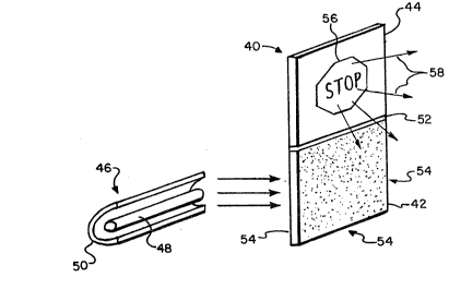
Referring to FIG. 3, a visual display device embodyin~
the present invention is generally designated by the
reference numeral 40. It comprises a light emitter panel
42 and a light display panel 44. The light emitter panel
42 preferably comprises a fluorescent dye-doped polymer
film or sheet of the type discussed in detail hereinabove.
~Although the emitter panel 42 is illustrated as being in
the form of a flat plate or panel, it may be curved or g
formed into any other desired shape as desired for a
particular application.
Further illustrated in the FIG. is a light source 46 ~ `
which comprises a commercially available green fluorescent ;
: ~: . :
A~
~ .,
ll
lamp 48 of the type discussed in det~il hereinabove, and a
mirrored reflector 50 for concentrating light emitted from
the lamp 48 toward the surface of the emitter panel 4~.
Although not visible in the drawing, all edge surfaces 54
of the emitter panel 42( except for the upper edge which is
attached to the visual display panel 44 by an optical
adhesive 52) are coated with an opaque or reflective
material to prevent light propagating through the emitter
panel 42 from exiting through the coated edges. Thus, the
emitter panel 42 constitutes a linear edge-emitting light
coupler which absorbs light emitted from the source 46 and
emits light into the display panel 44 through the adjoining
edges. Although an auxiliary light source 46 is
illustrated in the Figure, it is within the scope of the
invention to configure the visual display device 40 to
operate just with ambient light. In such a case, all light
incident on both the front and back surfaces of the emitter
panel 42 will be absorbed by the panel 42, and em;tted
thereafter through edge coupling into the display panel 44.
The intensity of the visual display produced by the panel
44 will be self-regulating, or more specifically,
proportional to the intensity of ambient light incident on
the emitter panel 42.
In a preferred embodiment of the present invention,
the emitter panel 42 absorbs green light from the
fluorescent light source 46 and emits light in the red
region of the visible spectrum. This embodiment is ideally
suited for a center-high-mounted stoplight application.
The visual display panel 44 is generically illustrated
as being in the form of a panel or plate with an exemplary -
"STOP" pattern 56 formed thereon. In practice, the display
panel 44 may be constituted by a polymer dispersed (PDLC) ~ -~
or other liquid crystal display, volume or other type of
hologram, or a plastic sheet or plate with an appropriate
pattern 56 formed on one surf=ce thereof. however, the
. ':
l ..
Z0060~;0 ~
12
PDLC embodiment will not be transparent in the off-state.
In the latter case, the pattern S6 may be formed by any
means which constitutes a distortion on the surface of the
panel 44 which changes the incident angle of the light
propagating through the panel 44. When the incident angle
is smaller than the total internal reflection angle, the
light will be directed out the surface of the panel 44 as
indicated by arrows 58.
: - .
Regardless of the particular configuration of the ;~
visual display panel 44, the optically transparent
substrate or host material of the panel 44 is preferably
selected to have substantially the same index of refraction
as the material of the emitter panel 42 and the material of
.. :;: ~
the optical adhesive S2 to ensure maximum internal
reflection and linear coupling of light from the emitter
panel 42 into the display panel 44, as well as maximum
transmission of light through the edge coupl ng interface
of the panels 42 and 44 and optical adhesive 52. ;~
Although the visual display panel 44 is illustrated
as being flat, it may be curved or formed into any desired
.. . ...
shape to suit a particular application. It is understood
that where the pattern 56 is formed on only one surface of
the display panel 44, the panel 44 will be transparent in
the absence of illumination incident on the emitter panel
42. Upon application of applied illumination from the
source 46, the display panel 44 will emit visible red light
through the areas of the pattern 56 only in the direction
of the arrows 58, while remaining transparent in the
opposite direction. Thus, the panel 44 may be adhered
directly to a rear window of an automotive vehicle and be
transparent to the vehicle operator under all conditions.
The red stop display will be visible only to operators of
~ vehicles approaching from the rear upon energization of tile
; light source 46 in response to application of the vehicle
3S brakes.
, . :~
: ~.~''.,`',"
. ~ ..
. . " ~
~1 ~Z ~
200~0
FIG. 4 illustrates a visual display device 60 in
accordance with the present invention which comprises an
emitter panel 62 in the form of two U-shaped sections 62a
and 62b. Each section 62a and 62b embraces one or more
fluorescent lamps 64, whereby light emitted by the lamps 64
is incident on the inner surfaces of the respective
sections 62a and 62b. All edges 62e and 62f of the emitter
panel sections 62a and 62b except for linear light coupling
edges 62c and 62d may be coated with an opaque or
reflective material to prevent light propagating through
the sections 62a and 62b from exiting the emitter panel 62
therethrough, although the scope of the present invention
is not limited to such a requirement.
The visual display device 60 further comprises a
display panel 66 which includes a polymer dispersed liquid
crystal (PDLC) module 68. Although the detailed component
elements of the module 68 are well known in the art and not
illustrated in detail, the module 68 generally comprises a
thin film 68a of PDLC. IT0 (indium tin oxide) conductive
films 68b are formed on the opposite surfaces of the PDLC
68a electrically active the module 68. The display panel
66 also has glass plates 70 which sandwich the module 66
for protective purposes.
The visual display device 60 may be operated in
darkness with the illuminating light edge coupled into the
¦ upper and lower edges of the PDLC display panel 66, as
illustrated. The device 60 may be operated in transmission
or reflection mode with auxiliary illumination placed in
front or in back of the display. In the latter case, the
fluorescent dye-doped polymer film emitter panel 62 for
edge-illuminating the display 66 increases the light output
and contrast between the electric field activated on and
off-states; this is equivalent to the contrast between the
dark background and bright symbols of the display.
' ' ~ '
"
~ .
i '~.. ZI'i'".'. ' ' .' ~ ' "
~, ';`~,`'~'; ''',',., ' ' ,
2~060~0
14
The PDLC films were known to be designed for optimum
viewing and illumination both at 90' to the film surface,
and at other angles. In the 90 position the electric
field aligned LC ordinary index is matched to the polymer
index, making the film highly transparent. Illumination at
less or greater than a 90 angle decreases the index match
and should reduce the contrast ratio. However, the higher
contrast results obtained with edge lighting were not
predictable, obvious or expected.
Major advantages resulting from edge lighting of a
PDLC display in the present novel manner include higher
brightness, better contrast, simple and high efficiency
piping of light into the display, application for ambient
light concentration, simple introduction of light into the
display and space saving features in automotive displays at
low cost. The measured absorbance of an 1/8 inch thick
phosphor luminescent plastic sheet can potentially exceed
99.9% over the main part of the spectrum. Thus, the light
power conversion efficiency of the total structure can have
a value in excess of 50%.
A modification of the visual display panel 66 is
illustrated in FIG. 5 and designated by the reference
numeral 66'. The component parts of the panel 66' are
essentially similar to those of the panel 66. However, the
panel 66' further comprises fluorescent dye-doped polymer
films 72 coated with conductive ITO films 68b. The films
72 in combination with the ITO films 68b form a refractive
index discontinuity at any mismatched interface thereof,
which causes ambient as well as edge-coupled ligh~
propagating therethrough to be scattered through the PDLC
module 68. This mechanism is similar to that described in
the reference to Baur and Greubel which was cited above,
and enhances the brightness, contrast and efficiency of the
visual display device.
Referring now to FIG. 6, another visual display device
Z0060S0
embodying the present invention is generally designated by
the reference numeral 80 and comprises an emitter panel 82
and a display panel 84. The emitter panel 82 is
essentially similar to the generic embodiment described
with reference to FIG. 3, and comprises a fluorescent dye-
doped polymer film plate with a mctallic coating 88 on
edges thereof which are not used for linear edge-coupling
of light into the display panel 84.
The display panel 84 comprises a plastic sheet or
plate formed with a pattern formed on one surface thereof
comprising thickness variations in the form of grooves 90.
Although it is within the scope of the present invention to
replace the grooves 90 with projections which serve the
identical function of coupling light out the surface of the
display panel 84, the grooves 90 may be easily formed by
engraving or etching. As discussed hereinabove, any
distortion or thickness variation on the surface of the
panel 84 which causes light propagating therethrough to be
incident on the distortion at an angle smaller than that of
the angle of total internal reflection will cause the light
to be reflected or scattered from the distortion out the
face of the panel 84 on which the distortiGn is formed.
Although the grooves 90 which constitute the visual light
output pattern are illustrated as being formed on only one
surface of the panel 84, the same or a different pattern
may be formed on the opposite surface thereof providing the
same or a different visual display depending on which
surface of the display panel is viewed.
FIG. 7 illustrates another embodiment of the present
invention in which a pattern 94 comprising printing is
formed on a surface of a plastic display panel 92. The
printing 94 comprises white or other colored ink which
creates an index of refraction discontinuity at the
interface of the ink with the surface of the panel 92
causing light propagating through the panel 92 to be
'!
~ ':
. ~'
Z006050
16
reflected or scattered out the surface thereof opposite to
the surface on which the printing 94 is applied. The
printing 94 may alternatively comprise light reflecting or -
light dispersing ink, and may be applied to the surfaces of
the grooves 90 in the embodiment of FIG. 6 if desired.
FIG. 8 illustrates an alternative embodiment of the
present invention in which the display pattern is in the
form of a ruled optical diffraction grating 98 formed on a
surface of a plastic display panel 96 for coupling light ~--
out the surface of the pattern. The grating may be 98 be
formed by photolithography, injection molding, machining,
or any other applicable manufacturing process, and has a
periodicity matched to the propagation direction and ~ ~`
wavelength range of the output light. Further, the grating
98 may be constituted by a volume or other suitable
holographic configuration. -
As discussed hereinabove, an emitter panel which
constitutes one of the components of the present invention
need not be in the form of a flat rectangular plate. The - ~
emitter panel may be formed in any desired shape by ~ `
injection molding OL' other applicable manufacturing process
as illustrated in the examples of FIGs. 9 and 10.
In FIG. 9, an emitter panel 100 is formed in the shape
of a spiral edge-emitting sheet, with a green fluorescent
lamp 102 provided inside the spiral shape and extending ;,,~
coaxially therein.
FIG. 10 illustrates an emitter panel 104 in the form
of an edge-emitting sheet formed into a generally ;
cylindrical shape with adjacent light coupling edge
sections 104a and 104b extending radially outwardly from a : -~
center of the cylindrical shape. The overall configuration
resembles a teardrop. The fluorescent lamp 102 is disposed
coaxially inside the panel 104. The radius of curvature of ;
the junctions between the main cylindrical portion of the
panel 104 and the edge sections 104a and 104b is made as
',, ' ' ", ~'.
~ '
6~50
17
large as is practically possible in order to facilitate
minimum loss propogation and total internal reflection of
light throughout the entirety of the emitter panel 104. In
both embodiments of FIGs. 9 and iO, the edges of the
emitter panels which are not used for output light coupling
are preferably coated with a light blocking reflective or
opaque material.
In furtherance of the PDLC liquid crystal display
embodiments described with reference to FIGs. 4 and 5, the
display may be placed in a thick polymer frame, where light
is introduced at 3 or 4 edges of the display, using
commercially available polymer films, or a frame molded
from dye doped pellets of this material. The electric
field aligned clear area of the display does not affect the
travel of light, or more specifically light introduced at
the edge which is being internally reflected from the front
and back of the glass surfaces, without being transmitted
through the glass/ITO surfaces. If there is a light
scattering medium in the light path, for example li~uid
crystal bubbles of the non-activated PDLC film, then the
direction of the light path will be changed. If the angle
at the surface is less than the angle of total reflection,
then the light is refracted and will leave through the
glass surface, as illustrated in FIG. 4.
A variation of the above technique is the use of a
very thin large surface area polymer film withln the
display cell as a light collector and internal spacer film.
Thin films of 3.6 mil may be molded from LISA pellets in a
150C pressurized cylinder at 1500 PSI.
The fluorescent dye doped polymer film can be ITO
coated by sputtering, and used as a conductive substrate
for PDLC fabrication as illustrated in FIG. 5. The light
collected over the entire surface area of the polymer film
will be redirected as fluorescent front face light at the
scattering non-activated areas of the PDLC, where the total
.;
,.
.~,
~' . .
!
~0t~6050
18
reflection is broken.
The above methods can all be used in the transmission
mode and the reflection mode. For reflective displays one
of the substrates would be replaced with a front surface
mirror or any other reflective type electrode.
Transmission mode display with an external transflector can
be used as a see-through daylight display and a reflective
night display.
EXAMPLE
A PDLC test cell was fabricated from a 1:1 mixture of - -
Norland 65 monomer and BDH-E7 liquid crystal in an ITO
coated test cell with a 1/2 mil Mylar spacer. The LC phase ;~
separation was completed after a 5 minute ultraviolet
exposure of the sample in a 200 watt mercury lamp system.
A 0.014 x 3.75 x 5.00 inch green LISA film was coupled to
two edqes of the test cell with optical cement. Electro~
optical measurements were taken normal to the sample using
a photodetector with two types of sample illumination~
1. Backlighting through Corning 4-64 filter.
2. Backlighting through Corning 4-64 filter + two -
fiber optic (FO) spot light illumination of the LISA ~-
plastic film.
The effect of illumination intensity on the on-state
brightness and contrast ratio is summarized in the ~
following TABLE. i
The contrast ratio (CR) is defined as:
CR = ( 100-Tor) / ( l~Ton)
TABLE
FO INTENSITY % TRANSMISSION CONTRAST RATIO
mw/cm2 Q70 VOLTS Q70 VOLTS
FIBER OPTIC ILLUMINATION OFF ON OFF ON
1.93 84.8 9G.8 6.54 8.91
2.89 84.2 93.0 6.29 10.40
3.67 84.5 9~.3 6.35 32.88 ~-
While several illustrative embodiments of the
, . .~.',: . .:
" ' ' :, ':
~' ~ ','
. ~
.~
`;!J ~ '
~,j: ' .
Z~06050
19
invention have been shown and described, numerous
variations and alternate embodiments will occur to those
skilled in the art without departing from the spirit and
scope of the invention. For example, the single emitter
panel which has been described and illustrated may be
replaced by a plurality of emitter panels, each emitting
light of a different color, to provide a multi-colored :- -
display device. Accordingly, it is intended that within
the scope of the appended claims the invention may be :
practiced otherwise than as specifically described.
'
', '
:
: '
: :