Note: Descriptions are shown in the official language in which they were submitted.
2~al6~:4~
LIQUID CRYSTAL DISPLAY DEVICE
The present invention relates to a liquid crystal device
allowing multi-gradation display.
PRIOR ART
A liq~lid crystal display device is disclosed in JA
Published Unexamined Patent Application (PUPA) No.
58-220185, in which one display unit is constituted by
four pixels 101, 102, 104, and 108 with area ratios of 1
: 2 : 4 : 8, allowing 16 gradation (gray scale) display
by the combination of the selection and non-selection of
the foux pixel~.
Also, since the light transmission factor of a liquid
crystal varies when a voltage applied to the liguid
crystal is varied, it is considered theoretically po~sible
to obtain a required gradation by varying a voltage
applied to a liquid crystal.
PROBLEMS TO BE SOLVED BY THE INVENTION
The prior art in said PIJPA No. 220185 ha~ to form a
pixel 108 having an area eight times that of the pixel
101, which is the smalle~t area, has a limit for
decrea~ing the area of one display unit, and can not be,
therefore, appl:ied to a liquid crystal display device
having high resolution and a large area.
JA9-88-029
2~06~4
Since change in the light transmission factor of a
liguid crystal is very large for a change in a voltage
applied to a liquid crystal, it is necessary to provide
electronic circuits operating with very high pre~ision in
order to obtain many gradations by adjusting a voltage
applied to a liquid crystal, which are very difficult -to
attain.
An object of the present invention is to provide a
liquid crystal display device which allow~ multi-gradation
display to be attained by only selection of application
and non-application of a voltage to a liquid crystal
without needing to increase an area of one display unit
and without needing to finely adjust the value of voltage
applied to the liquid crystal of each pixel.
MEANS FOR SOLVING THE PROBLEMS
In a liquid crystal display device in which the
application of a voltage to a li~uid crystal for each
pi~el is controlled, in accordance with the present
invention,
one display unit is constltuted with n (n is a
positive integer) adjacent pixels;
a light transmi~sion ~actor control layer for
controlling the liyht transmission factor of the pixel i~
provided for each pixel; and
the ratio between light transmission factors of light
transmission factor control layers of n pixels in one
JA9-88-029 2
2(~0~i~49L
display unit is set as ollows: 2 : 21 : 22 2n-
whereby a 2n gradation display is allowed.
BRIEF DESCRIPTION OF THE DRAWINGS:
Fig. 1 is a perspective view showing one embodiment
of a liquid cry~tal display device according to the
present invention;
Fig. 2 is a diagram illustrating the relation between
display units of the liguid crystal display device shown
in Fig. 1 and pixels; ~ A
Fig. 3 is a diagram illustrating the fact that the
combinations of the light transmission and interception ;
of four pixels in one display unit of the liguid crystal : .
display device shown in Fig. 1 allows 16 gradations to be
obtained; ~
Fig. 4 is a graph showing the relation between a RPM . :
and a light transmission factor in the case where a
reguired light transmission factor is obtained by rotative
painting;
Fig. 5 is a diagram illustrating the relation between
a display unit of another embodiment according to the
present invention and pixels;
Fig. 6 is a diagram illustrating the fact that the
combinations of the light transmission and interception ..
of the three pixels in the display unit shown in Fig. 5
allow~ eight graclation~ to be obtained; and
JA9-88-029 3
`
: .
, .... .... .. ... . ~ ... . .. .. .
Z~ 4~
Fig. 7 is a diagram illustrating the relation between
the display unit and the pixeil according to the prior art.
EMBOD I MENT
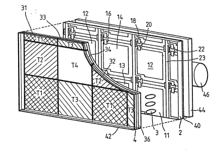
Eig. 1 shows an embodiment of a lic~uid crystal
di~play clevice according to the present invention which
realizes 16 gradations. In the embodiment, a display unit
DU of a licluid crystal display device is made to be a
square, and the clisplay unit DU is composed of four pixels
Tl, T2, T3, and T4 located at positions of four squares
formed by dividing the scluare into four egual parts as
shown in Fig. 2.
Re~erring to Fig. 1, regions corre~ponding to the
pixels Tl, T2, T3, and T4 in Fig. 2 in a transparent glass
substr~te 2, what i~ called the TFT array subskrate, are
provided with transparent pixel electrodes 11, 12, 13, and
14 made of ingium tin oxide (hereinafter called IT0). The
pixel electrodes 11, 12, 13, and 14 are respectively
connected to source electrodes 20 of thin-film transistors
(hereinafter called a~Si TFT) 16 macle of amorphous
silicon, each of which controls the application of a
voltage to a liquid crystal in the pixel region. The a-Si
TE'T 16 is connected at its gate electrode (not ~hown) to
an address wiring 22, and at its drain electrode 18 to a
data wiring 23. Al#o, a liquid crystal orientation film
(not shown) i~ provided ranging over the whole c)f the
substrate 2 insicle the pixel electrode 12.
JA9-8~o?g 4
Z44
A transparent glass substrate 4, which i5 called the
counter substrate, is disposed so as to be opposite to the
TFT array substrate 2. Inside the counter substrate 4
(that is, on the side toward the TFT array substrate 2),
light transmission factor control layers 31, 32, 33, and
34 are provided. The light transmission factor control
layer~ 31, 32, 33, and 34 are disposed in the regions of
the pixel Tl, T2, T3, and T4 shown in Fig. 2,
respectively, and the ratio between light transmission
~actors of the layers is set to 2 ~ : 23, that
is, ~ : 2 : 4 : 8.
In5ide the light transmission factor control layers
31, 32, 33, and 34 (that is, on the side toward the TFT
array substrate3, a common electrode 36 is provided all
over the whole surface of the counter substrate 4. Inside
the common electrode 36 a liquid crystal orientation film
(not shown) is provided over the whole surface of the
substrate 4. A liquid crystal 3 is filled between the TFT
array substrate 2 and the counter substrate 4, i more
correctly ~peaking, between an orientation film provided
on the pixel electrodes 11, 12, 13, and 14 and an
orientation film provided on the common electrode 36. At
the rear of the TFT array substrate 2 i~ provided a back
illumination source 46, and outside the TFT array
~ubstrate 2 (that i 9, on the s.ide toward the back
lllumination source 46) is provided a polarizing plate 40.
Between the bacX illumi.nation source 46 and the polarizing
plate 40 is a diffusion plate 44 ~or diffusing light.
JA9-88-029 5
:.
~ .
" . . . . .. .. .
21)C)~iZ~L4
Also, outside the counter electrode 4 (that is, on the
opposite side of the TFT array substrate 2) is provided a
polarizing plate 42.
Upon the application of a gate pulse to the address
wiring 22, the a-Si TFT 16 on the wiring 22 is placed in
the ON state, and a data voltage on the data wiring 23 at
that time i9 applied to the liquid crystal 3. Assuming
that the directions of the polarizing plates 40 and 42 of
the liquid crystal display device ~hown in Fig. 1 are
parallel with each other and the molecular axis of tha
liquid crystal is twistecl by 9O0 in a state that no voltage
is applied to the licluid crystal 3, when the data voltag0
is applied to the liquid crystal 3, the molecular axis of
the licluid crystal is made parallel and light passes
through the lic~id crystal. Assuming that the directions
of the polarizing plates 40 and 42 of the licluid crystal
display device in Fig. 1 are perpendicular with each other
and the molecular axis of the liquid crystal is twisted
by 9O0 in a stake that no voltage is applied to the liquid
crystal 3, when no voltage is applied to the liquid
crystal, the liquid crystal allows light to pass through
it, and on the contrary, when a voltage is applied to the
liquid crystal, the molecular axes of the lic~id crystal
are parallel with each other and the liquicl crystal
intercept~ light. In both cases, the ON-OFF contxol of
the a-Si TFT 16 allows the light tran~mission and
interception thrc)ugh the liquid crystal of each pixel to
be controlled.
JA9-88~029 6
In this way, the application of voltages to the
pixels Tl, T2, T3, and T4 can be independently controlled
by the a-Si TFT 16, and the light transmission and
interception can be also independently controlled.
Accordingly, sixteen different combinations of light
transmission and interception in the pixels Tl, T2, T3,
~, and T4 are available, as shown in Fig. 3.
~i Fig. 3(a) shows a state in which all of the pixels
Tl, T2, T3, and T4 intercept light. The amount of light
transmission of the whole display unit DU in this case is
as follows, as a relative value:
. o = O
l + 2 + 4 + 8 15
.
! Fig. 3(b) shows a state in which the pixel Tl allowslight to pass through it, and the pixels T2, T3, and T4
intercept light. The amount of light transmission of the
whole display unit DU in this case is as follows, as a
relative value:
___ _ .
3 l ~ 2 ~ 4 + 8 15 ~
.~ ,.
Fig. 3(c) shows a state in whi~h the pixel T2 allows
light to pass through it and the pixels Tl, T3, and T4
JA9-88~029 7 ~
,:
~.
~o~
intercept light The amount of light transmission of the
whole display unit DU in this case is a~i follows, as a
relative value:
2 = 2
' ;-
1 + 2 + 4 + 8 15
Fig. 3(d) shows a state in which the pixel T3 allowslight to pass through it and the pixels Tl, T2, and T4
intercept light. An amount of light transmission of the
whole display unit DU in this case is as follows, as a ;.~ ~
relative value: ~ -
4 = 4
1 + 2 + 4 + 8 15 ::
,. '~
Fig. 3(e) shows a state in which the pixel T4 allows
light to pass through it and the pixels Tl, T2, and T3
, i ,.... ...
intercept llght. The amount of light transmission of the
whole display unit DU in this case is as follows, as a
relative value:
. j .
8 = 8
.... _ ..... _ :,
1 + 2 + 4 + 8 15
JA9-88-029 8
.
Fig. 3(f) shows a state in which the pixels T1 and
T2 allow light to pass through them and the pixels T3 and
T4 intercept light. The amount of light transmission of
the whole display unit DU in this case is as follows, as
a relative value:
1 + 2 = 3
1 ~ 2 + 4 ~ 8 15
Fig. 3(g) shows a state in which the pixels T2 and
T3 allow light to pass through them and the pixels Tl and
T4 intercept light. The amount of light transmission of
the whole display unit DU in this case is as follows, as
a relative value:
2 + 4 = 6
1 ~ 2 + 4 + B 15
Fig. 3(h) shows a state in which the pixels T3 and
T4 allow light to pass through them and the pixels Tl and
T2 intercept light. The amount of light transmission of
the whole display unit DU in this case i9 as follows, as
a relative value:
JA9-88-029 9
~o~
4 ~ 8 - 12
1 ~ 2 ~ 4 + 8 15
Fig. 3(i) shows a state in which the pixels T1 and
T3 allow light to pass through thlem and the pixels T2 and
T4 intercept light. The amount of light tra~smis~ion of
the whole display unit DU in this case is as follows, as
a relative value:
1 ~ ~ - 5 ~ ~
'.:
1 + 2 ~ 4 + 8 15 -~ -
Fig 3(j) shows a state in which the pixels T2 and T4
allow light to pass through them and the pixels Tl and T3 ~ ;
intercept light. The amount of light transmission of the
whole display unit DU in this case is as follows, as a
relative value: ,
2 ~ 8 = lO
1 + 2 ~ 4 ~ ~ 15
Fig. 3tk) shows a state in which the pixels T1 and
T4 allow light to pass through them and the pixels T2 and
T3 intercept light. The amount of light transmlssion of
.:
JA9-88-029 10 ~
. , .
~0~62~4
the whole display unit DU in this case is as follows, as
a relative value:
1 + 8 = 9
1 + 2 ~ 4 ~ 8 lS
Fig. 3(l) shows a state in which the pixels T2, T3,
and T4 allow light to pass through them and the pixel Tl
intercepts light. The amount of light transmission of the
whole display unit DU in this case is as follows, as a
relative value:
2 ~ 4 + 8 = 14
_ ~ . .
1 1 2 ~ 4 + 8 15
Fig. 3(m) shows a state in which th~ pixels T1, T3,
and T4 allow light to pass through them and the pixel T2
intercepts light. The amount of light transmission of the
whole display unit DU in this case is as follows, as a :~
relative value:
~ + 4 ~ 8 = 13 :
1 ~ 2 + 4 ~ ~ 15 .~:
JA9-88-029 11
24'~
Fig. 3(n) shows a state in which the pixels T1, T2,
and T4 allow light to pass throuqh them and the pixel T3
intercepts light. The amount of light transmission of the
whole display unit DU i~ this case is as follows, as a
relative value:
1 + 2 ~ 8 = 11
1 ~ 2 + 4 + 8 15
.. ............. .
Fig. 3~o) shows a state in which the pixels T1, T2,
and T3 allow light to pass through them and the pixel T4
intercepts light. The amount of light transmission of the
whole display unit DU in this case i5 as follows, as a
relative value:
l + 2 + 4 = 7
_
1 ~ 2 + 4 ~ 8 15
Fig. 3(p) shows a state in which all the pixels T1,
T2, T3, and T4 allow light to pass through them. The
amount of light transmission of the whole display unit DU
in this case is as follows, as a relative value:
1 ~ 2 + ~ + 8 - 15
1 ~ 2 + 4 + 8 15
JA9-88~029 12
. . .
- ; ! ,i ; ~ ~ , :
44
As apparent from the above description, if the ratio
of the light transmission factors of the pixels Tl, T2,
T3, and T4 is left to be 1 : 2 : 4 : 8, the combination
of the light transmission and interception of the pixels
Tl, T2, T3, and T4 allows the relative amount of light
transmissions of 0/15, 1/15, 2/15, 3/15, 4/15, 5/15, 6/15,
7/15, 8/15, 9/15, 10/15, 11/15, 12/15, 13/15, 14/15, and
15/15 to be obtained, which allows 16 gradations to be
attained.
In order to make the ratio of the light transmission
factors of the pixels T1, T2, T3, and T4 be 1 : 2 : 4 :
8, the light transmission factors of the light
transmission factor control layers 31, 32, 33, and 34 need
only to be, for example, 12.5%, 25.0%, 50.0%, and 100~.
This can be realized, for example, by controlling an
amount of dispersion of carbon black into the acrylic
resin. For example, a standard solution (hereinafter
called a STD solution) produced by adding a
photopolymerization initiator and carbon black to acrylic
resin and performing viscosity adjustment, and dilution
thereof is rotatively applied with painting at speeds of
520 RPM and 900 RPM, allowing the light transmission
factors o 12.5% and 25.0% to be obtained. When the STD
solution diluted :in such a manner that the carbon black
component amount:ing to 30% is rotated at the speed of 650
RPM, the light transmissi.on factor of 50.0% can be
obtained.
JA9-88-029 13
6~:4a~
Fig. 4 shows the relationship between the revolutions
per minute and a light transmission factor in the ca~e
where a required light transmission factor is obtained by
rotative painting. As described abov2, if resin
components are provided with photosensitivity by adding a
photo polymerization initiator, ,patterns can be obtained
by only development. Resin components having no
~ photosensitivity is painted thereon with a photoresist,
! applied with patterning by use of a conventional
technique, and then can be processed with etching.
Fig. 5 shows an example of an arrangement of pixels
in the case where one display unit is composed of three
, adjacent pixels. Three square-shaped pixels Sl, S2, and
I S3 located at each apex of a inverse regular triangle
compose one display unit, and the ratio of its light
transmission factors is
" '. ,.'.
1 2 21 22
¦ that is,
~ , ';.
~ 2 : 4.
'''';'
In the case of this arrangement of pixels, eight :
combinations of the light transmission and interception
of the pixels Sl, S2, and S3 are available, as shown in
, Fig. 6.
JA9-88-029 14
:
.: '
~ 0~24~
Fig. 6(a) shows a state in which all of the pixels
Sl, S2, and S3 intercept light. The amount of light
transmission of the display unil: DU in this case is as
follows, as a relative value:
o = o
.
~ 1 + 2 ~ 4 7
:..
1, Fig. 6~b) shows a state in which the pixel Sl allows
light to pass through it and the pixels S2 and S3
intercept light. The amount of light transmission of the
display unit DU in this case is as follows, as a relative ¦ -
value: -
'
= 1
l ~ 2 + 4 7
Fig. 6(c) shows a state in which the pixel S2 allows
light to pass through it and the pixels Sl and S3
¦ intercept light. The amount of light transmission of the
i display unit DU in this case is as follows, as a relative
valu~:
2 = 2
1 ~ 2 + 4 7
JA9-88-029 15
z~
Fig. 6~d) shows a state in which the pixel S3 alloms
light to pass through it and the pixels S1 and S2
intercept light. The amount of light transmission of the
display unit DU in this case is as follows, as a relative
value:
4 = 4
1 + 2 + 4 7
. ~ . .
Fig. 6(e) shows a state in which the pixels S1 and -
S2 allow light to pass through them and the pixel S3
intercepts light. The amount of light transmission of the
display unit DU in this case is as follows, as a relative
value:
: . ~
1 + 2 = 3
; " - .
1 ~ 2 ~ 4 7
. .
Fig. 6(f) ~hows a state in which the pixels S1 and ~ ~;
S3 allow light to pass through them and the pixel S2
intercepts light. The amount of light transmission of the
display unit DU in this case is as follows, as a relative
value:
JA9-88-029 16
6~44
1 -~ 4 = 5
1 + 2 + 4 7
Fig. 6(g) shows a state in which the pixels S2 and
S3 allow light to pass through them and the pixel S1
intercepts li~ht. The amount of light transmission of the
display unit DU in this case i3 as follows, as a relative
value:
4 = 6
,."':
1 ~ 2 + 4 7 .:
Fig. 6~h) shows a state in which all the pixels Sl,
S2, and S3 allow light to pass through them. The amount -
of light transmission of the display unit DU in this case
is as follows, as a relative value:
1 ~ 2 + 4 = 7
_
1 + 2 ~ 4 7
In this way, even if three pixels compose one diæplay
unit, if the ratio of the light transmission factors of
the three pixels is made to be 1 : 2 : 4, the combinations
of the light transmission and interception of the three
pixels allows the relative amount of the light
JA9-88-029 17
`:'.'
,~
,~ '; :
... .. ... . .. . . .. . . . .. . . . .. . ..
~0~6~
transmissions of 0/7, l/7, 2/7, 3/7, 4/7, 5/7, 6/7 and 7/7
to be obtained, which allows eight gradations to be
attained.
The above-mentioned embodiments are those in the
cases where one display unit is composed of four and three
pixels. The present invention is not limited by the
number of these pixels, and can be applied to the case
where one display unit is composed of n (n is a positive
integer) pixels. In other words, since a pixel for
forming one display unit can not be any value except the
two values of ON (light transmission) and OEF (light
interception), when the ratio of the light transmission
.
factors of these pixels is decided in accordance with two
exponential functions (2x : x = O, 1, 2, the
multi-gradations become most linear. Accordingly, the
ration of light transmission factors of n pixels needs
only to be 2 2l 22... 2n-
In the above-mentioned embodiment, although a TFT is
employed as a switching element which controls the
application of voltages to liquid crystals in a pixel
domain, the present invention is not limited by this, but,
for example, MIM (metal - insulator metal) can be
employed.
Al~o, the present invention can be applied not only
to the above-mentioned so-called active matrix type liquid
crystal, but also to a simple matrix type liquid crystal.
The reason is that in a simple matrix type, the
application of voltage~ to pixels in the region where an
JA9-88-029 18
~ . . .. .. .. .
2~24~
X electrode and a Y electrode intersect is selected to
control light transmission and :interception for liquid
crystals in the pixel region concerned.
Also, in the above-mentioned embodiment, a light
transmission factor control layer is provided on the side
of the counter electrode 4, it may be provided on the
pixel electrodes on the substrate on the side of the
switching elements such as TFT. `
The present invention allows a multi-gradation
display without the necessity of enlarging an area in one
display unit, or of finely adjusting voltages applied to :
the liguid crystals in each pixel.
JA9-88-029 19
. ,