Note: Descriptions are shown in the official language in which they were submitted.
TIThE OF THE INVENTION
Synchronization Recovery Circuit for Recovering Word
Synchronization and Radiocommunication Apparatus Using the
Same
BACKGROUND OF THE INVENTION
Field of the Tnvention
The present invention generally relates to
synchronization recovery circuits and radiocommunication
apparatuses,using such circuits, and more particularly, to
a synchronization recovery circuit which detects a word
synchronizing character in a received data signal for
recovering word synchronization in a cellular--type
communication system, and to a radiocommunication
apparatus such as car telephone and portable telephone -
~15 using such a synchronization recovery circuit.
Description of the Prior Art
A cellular-type communication system has been widely
utilized in the form of a mobile radio telephone such as
car telephone or portable telephone. In such a
cellular-type communication system, an area to be covered
is divided into multiple cells, each of which is provided
with a radio base station and assigned a group of
channels. Such a small-sized service area of each cell
and reduced transmission output of a base station enable
frequent reuse of the frequencies, admitting an increased
number of subscribers.
zn such a cellular-type communication system, when a
mobile station equipped with a radiocominunication
apparatus, for example, an automobile equipped with a car
telephone moves .from one cell to another, several kinds of
digital control including channel change or the like are
performed in order that complete communications are
established between the radio base stations involved and
the car telephone apparatus.
Each radio base station has two types of .radio
channels, one of which is a bidirectional control channel
for such several kinds of digital control as mentioned
above, and the other is a bidirectional audio_channel for
conversation over the telephone.
For such bidirectional communications, four channel
types are employed. More particularly, the control
channel comprises a forward control channel (FOCC) used
for communication from a radio base station to a mobile
station and a reverse control channel (RECC) used for
communication from a mobile station to a radio base
station, which are generally used for control of every
kind before the audio channel is established, and not for
conversation. On the other hand, the audio channel
comprises a forward audio channel (FVC) used for
2
~~~~~5~
communication from a radio base station to a mobile
station and a reverse audio channel (RVC) used for
communication from a mobile station to a radio base
station.
On these channels, a message, or a data signal
containing a word synchronizing character is transmitted
at predetermined word and bit rates. Therefore, a
radiocommunication apparatus of a mobile station is first
required to detect the word synchronizing character out of
a received data signal for recovering word
synchronization. For this purpose, in a conventional
xadiocommunication apparatus, as disclosed in the US
Patent No. 4,029,900, there is provided a synchronization
recovery circuit which detects the_word synchronizing'
character out of the data signal for recovering word
synchronizatibn. In this synchronization recovery
circuit, the word synchronization is recovered by
supplying a control circuit for data processing with a
word synchronizing signal which has been generated based
on the detected word synchronizing character.
The conventional synchronization recovery circuit,
however, is constituted in the light of its hardware
construction such that the word synchronizing signal is
serially applied to the control circuit. Therefore, in
order to recover word synchronization based on such a
_ 3
serial word synchronizing signal, also the data signal
must be serially applied to the control circuit. The
control circuit receives both of the word synchronizing
signal and the data signal serially and accepts the data
signal as effective data for use, only after a word
synchronizing position is identified. In the above
mentioned construction wherein the data signal is adapted
to be accepted after word synch-ionization is established,
data may possibly drop out due to high data transmitting
rate of the celluar-type communication system. Therefore,
the control circuit is always required to access the data
signal and thus can not do any other processing such as
key scan, LCD display, AF {Analog Frequency) processing,
radio-functional processing or the like during the access,
prevented from performing any kind of processing required
as a mobile station, at a higher speed.
As one solution to this problem, a control circuit
comprised of two microprocessors has been proposed, with
one microprocessor performing synchronization recovery of
the received data and the other performing any other
processing such as key scan. This has led to another
problem, however, that the two microprocessors require
additional complicated control such as communication
control (for example, determination of .communication
protocol) and timing control between themselves.
- -4 -
_ . .
i
~~~~~~~
Furthermore, a technology of converting the data
signal from serial form to parallel form before supplied
to the control circuit has been proposed in Japanese
Patent Laying-Open No. 63-245032. Since the word
' 5 synchronizing signal is supplied in serial form, however,
such a parallel data signal in itself does not allow
identification of a synchronizing position, so that any
software-controlled processing becomes indispensable in
the control circuit. More specifically, such
software-controlled processing may include a processing
for determining a synchronizing character pattern by
shifting a data signal bit by bit in order to identifying
the position of the synchronizing character in the
accepted data signal again. Therefore, with such a
technology, a higher operating speed of the
radiocommunication apparatus can hardly be attained.
SUMMARY OF THE INVENTION
An object of the present invention is to enable a
radiocommunication apparatus to perform processings at a
higher speed in a cellular-type communication system.
Another object of the present invention is to enable
word synchronization recovery of received data with
parallel signal processing in a radiocommunication
apparatus as a mobile station.
6
m 5 -
! _
~~~2~~
Briefly stated, according to the present invention,
serial data containing a predetermined word synchronizing
character is converted into first parallel data of n bits
(n is integer of 2 or more) while generating second
parallel data of n bits which indicates a word
synchronizing position in the first parallel data, and
based on these first and second parallel data, word
synchronization of the serial data is recovered.
The main advantage of the present invention is,
therefore, that since the received data signal and the
word synchronizing signal indicating the synchronizing
position thereof are both processed as parallel data, the
word synchronization can be quickly recovered and thus all
the processings required from a radiocommunication
apparatus can be done at a higher speed.
The foregoing and other objects, features, aspects
and advantages of the present invention will become more
apparent from the following detailed description~of the
present invention when taken in conjunction with the
accompanying drawings.'
BRIEF DESCRIPTION OF THE DRAWINGS
Fig. 1 is a diagram showing a typical format of a
forward control channel message.
g
Figs. 2 (a) and (b) are diagrams showing specific
examples of a bit synchronization field and a word
synchronization field, respectively.
Fig. 3 is a schematic block diagram showing a
radiocommunication apparatus according 'to an embodiment of
the present invention.
Fig. 4 is a block diagram showing an internal
structure of the data receiver in the radiocommunieation
apparatus shown in Fig. 3.
Fig. 5 is a diagram showing details of the
serial-parallel converter shown in Fig. 4.
Fig. 6 is a block diagram showing details of the
8-bit shift register shown in Fig. 5.
Fig. 7 is a block diagram showing details of the word
synchronization detecting circuit and the word
synchronization detecting shift register shown in Fig. 4.
Fig. 8 is a block diagram showing details of the
delaying circuit shown in Fig. 4.
Fig. 9 is a block diagram showing details of the
received data outgut port and ~k.he word synchronization
detection output port shown in Fig. 4.
Fig. 10 is a block diagram showing a structure of the
three-state buffer register shown in Fig. 9.
Fig. 11 is a timing chart for explaining operation of
the circuit shown in Fig. 4. '
- 7 -
~f ~~~
Fig. 12 is a diagram .for schematically explaining
operation principles of the circuit shown in Fig. 4.
Fig. 13 is a block diagram showing details of the
control circu:i~t shown in Fig. 3.
Fig. 14 is a flow chart fox explaining operation of
the microcomputer shown in Fig. 13.
Fig. 15 is a flow chart showing another example of
processing by the microcomputer shown in Fig. 13.
DESCRTPTIOPI OF THE PREFERRED EMBODIMENTS
In the following, an embodiment of the present
invention will be described with reference to the
accompanying drawings. The embodiment to be described
hereinafter is on a case where the present invention is
applied to the forward control channel (FOCG) among the
signal paths previously described. On this forward
control channel, a forward control channel message
(baseband data signal) is transmitted from a radio base
station to a mobile station (radiocommunication
apparatus), which will preform processings such as
registration, channel change or the like according to the
received message.
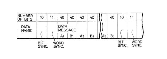
Fig. 1 is a diagram showing a typical format of such
a forward control channel message. This message is
largely composited of a bit synchronization field, a word
synchronization field and a data message. More
_ g
particularly, the bit synchronization field is, as shown
in Fig. 2 (a), a 10-bit field having alternate 1 and 0
bits recurrent in'sequence (known as dotting). The word
synchronization field in turn, as shown in Fig. 2 (b), is
a 11-bit .field having a bit arrangement which: is rarely
seen in the data message. In the United States, fer
example, the arrangement of "11100010010" as shown in Fig.
2 (b) is employed. Furthermore, the data message
comprises data messages A and B each having 40 bits, which
are alternately repeated 5 times for each (designated as
A1 to A5 and B1 to B5, respectively). Such 5-time
repetition of the respective data messages is for error
correction, i.e. for determining effectiveness of data
with a coincidence ratio of more than 3/5, or by majority
decision when there exists difference between the received
data.
Meanwhile, though not shown in Figs. 1 and 2, one
busy-idle bit is added to every 10 bits of the bit
synchronization field, the word synchronization field and
the respective data messages. This busy-idle bit serves
to inform a mobile station of whether the transmission
source of the message, or a radio base station is prepared
to receive, or of vacancy status of the reverse control
channel (RECC). Accordingly, the bit synchronization
field, the word synchronization field and 'the data message
- 9 -
are in practice comprised of 11 bits, 12 bits and 44 bits,
respectively. The message shown in Fig. 1 will be then
transferred, for example in the United States, at a 10
kilo bit/second rate after Manchester-encoded in the
well-known manner.
Subsequently, Fig. 3 is a schematic block diagram of
a xadioconununication apparatus as a mobile station in a
cellular system according to an embodiment of the present
invention. Tn the diagram, an antenna 3 is connected to a
receiver 1 and a transmitter 2 through an antenna coupler
4. The receiver 1 FM-demodulates a received signal which
has been received from a radio station with the antenna 3.
The receiver 1 applies a data signal on the forward
control channel to a data receiver 6 and a received audio
signal on the forward audio channel to an audio processing
cixcuit 5 by use of a discriminator not shown. The data
receiver 6 detects a word synchronizing character out of
the applied message of FOCC and applies a word
synchronizing signal to a control circuit 8 constituted of
a 8-bit microprocessor, along with the data signal. The
control circuit 8 identifies a synchronizing position of
the data signal, based on the applied word synchronizing
signal, before executing any kind of control according to
the data signal. The control circuit 8 performs
additional processing and control necessa~cy fox a key
10 _
~~~~~~~
matrix 11 or an LCD driver 12. On the other hand, the
audio processing portion 5 amplifies the applied message
of FVC for application to a handset speaker 10. This
enables a user of a mobile station to receive a
communication from another. Meanwhile, the control
circuit 8 performs control such as muting instruction also
for the audio processing circuit 5.
The data transmitter 7 Manchester-encodes a data
signal from the control circuit 8 for application to the
transmitter 2 as a message for RECC. Meanwhile, the audio
processing circuit 5 processes an audio signal applied
from a user through a microphone 9 for application to the
transmitter 2 as a transmitting audio signal for RVC. The
transmitter 2 FM-modulates these signals for transmission
to a base station by use of the antenna 3.
Meanwhile, a radio base station of each cell is
connected to a mobile telephone switching office (MTSO)
not shown through a conventional land line or a microwave
network. This MTSO is further connected to the public
switching telephone network (PSTN), establishing interface
between a mobile radio telephone and the PSTN.
Subseduently, Fig. 4 is a block diagram showing an
internal structure of the data receiver 6 shown in Fig. 3,
the respective parts of which axe shown in the block
diagrams of Figs. 5 to 10 in detail. Furthermore, Fig. 11
11
is a timing chart showing signals of the data receiver 6,
and Fig. 12 is a diagram for schematically explaining
operation principles thereof.
First, a forward control channel message transmitted
from a radio base station (not shown) is FM-demodulated in
the receiver 1 and extracted by an LPF 13. The analog
forward control channel message extracted by the LPF 13 is
digitalized by a limiter 601 before applied to a clock
signal generating circuit 602 and a Manchester decoder 603
as a data signal in Manchester code format. The clock
signal generating circuit 602 which is constituted of a
well-known PLL (Phase Locked Loop) circuit generates a
clock signal RT (Fig. 11(b)) which has been
bit-synchronized with the data signal-in Manchester code
format. This clock signal RT is applied to the Manchester
decoder 603 and an inverter 607, and also to a delaying
circuit 608 and a word synchronization detecting shift
register 621 as will be described later. On the other
hand, the Manchester decoder 603 converts, in response to
'the data signal and the clock signal RT, the data signal
from the Manchester code format to NRZ (Non Return to
Zero) format (Fig. 11(a)) and applies the converted signal
to a serial-parallel converter 604. This seacial-parallel
converter 604 has function of a 16-bit shift register and
- 12 -
thus converts the serial NRZ data from the Manchester
decoder 603 into parallel data of Z6 bits.
Fig. 5 is a diagram showing a structure of the
serial-parallel converter 604. As shov~in in the diagram,
the serial-parallel converter 604 is comprised of two
8-bit shift registers 605 and 606, and a clock terminal of
each shift register is supplied with output RT (Fig.
1J.(c)) of the inverter 607 in Fig. 4. Therefore, the
shift registers 605 and 606 both operate at a timing of
the RT. More particularly, the shift register 605
consecutively accepts the NRZ data at a timing of RT while
applying an output Q7 to a data input of the shift
register 606. This shift register 606 also consecutively
accepts the outpu~ Q7 of the shift register 605 at a
taming of RT. As a result, the NRZ data from the
Manchester decoder 603 is converted into 16-bit parallel
data QO to Q15, among which the 8-bit data QO to Q7
outputted from the shift register 605 are applied to both
of the delaying circuit 608 and the word synchronization
detecting circuit 631 while the 8-bit data Q8 to Q15
outputted from the shift register 606 are applied to the
word synchronization detecting circuit 611. Furthermore,
Fig. 6 is a diagram showing a structure of the 8-bit shift
register 605 or 606 shown in Fig. 5, comprising 8
2S flip-flops connected in series.
.. 13
~~~a~
Turning back to Fig. 4, the 16-bit output of the
serial-parallel converter 604 is applied to the word
synchronization detecting circuit 611> This word
synchronization detecting circuit 611 detects, based on
these data, a ward synchranizing character. More
particularly, the ward synchronization detecting circuit
611 detects a 15-bit word synchronizing character
composited of the last 4 bits of the bit synchronization
field and the 11 bits of the word synchronization field
shown in Figs. 1 and 2, i.e. "1010 (bit sync. field)
11100010010 (word sync, field)~. Though generally the
word synchronizing character may be composited of only the
10 bits of the word synchronization field, the increased
bit number of the word synchronizing character which has
the last 4 bits of the bit synchronization field added to
the original 10 bits of the word synchronization field as
described above can reduce the probability that the word
synchronizing character may happen to coincide with data
of the data message portion, enhancing the precision of
word synchronization detection. The output signal of the
word synchronization detecting circuit 611 is then
accepted by the word synchronization detecting shift
register 621 at a timing of the clock signal RT.
Fig. 7 is a diagram showing details of the word
25, synchronization detecting circuit 611 and the word
- 14 -
~~~t~
synchronization detecting shift register 621. In the
diagram, the word synchronization detecting circuit 611
comprises inverters 612 to 619 and an AND gate 620. The
AND gate 620 generates a logical product of the outputs of
the serial--parallel converter 604, or the outputs Q1, Q4,
Q8' Q9' Q10' Q13 and Q15, and signals obtained by
inverting the ou'tpu'ts QO' Q2' Q3' Q5' Q6' Q7' Q12 and Q14'
Meanwhile, since the output Q11 of the serial-parallel
converter 604 is the previously described busy-idle bit
which is unrelated to the word synchronization, it is not
connected to the ,AND gate 620. Therefore, only when the
outputs Q15 to Q12 and Q10 to QO of the serial-parallel
converter 604 take a value of "101011100010010" equal to
the above-mentioned l5;bit word synchronizing character,
all the inputs of the AND gate 620 become "1°', causing the
AND gate 620 to output °'1" indicative of detection of the
woxd synchronization character. The output of the AIdD
gate 620 is consecutively accepted by the word
synchronization detecting shift register 621 which is a
8-bit shift register as shown in Fig. ~, at a timing of
the clock signal RT, or delayed by a half cycle with
respect to the RT, for being converted into 8-bit parallel
data WSO to WS7. These 8-bit parallel data WSO to WS7 are
then applied to a word synchronization detection output
port 622. The output port 622 simultaneously latches the
8-bit input data at a timing of output RT8 (Fig. 11(d)) of
a frequency-divider 610 at which the output RT of the
inverter 607 is frequency-divided by 8.
Meanwhile, the outputs QO to Q7 0~ the 8-bit shift
register 605 in the serial-parallel converter 604 are
applied to the delaying circuit 608. The delaying circuit
608 is a 8-bit buffer register comprised of 8 flip-flops
as shown in Fig. 8 and simultaneously accepts the 8-bit
data QO to Q7 at a timing of the clock signal RT which has
been delayed by a hal~ cycle with respect to the RT. In
other words, this 8-bit register 608 is a timing register
which has been provided for establishing synchronization
with the word synchronization detecting shift register
621. The outputs RDO to RD7 of this shift register 608
are applied to a received data output port 509. The
outgut port 609, like the above-mentioned output port 622,
simultaneously latches the 8-bit input data at a timing of
the RT8 outputted from the frequency-divider 610.
Reading-out from the output ports 609 and 622 is
performed in response to address signals ARD and AWS from
a 2-bit address line 624 and a read-out signal ItD, and
output of each output port is applied to the control
cixcuit 8 of Fig. 3, through a 8-bit data bus 623.
Fig. 9 is a block diagram showing details of these
output ports 609 and 622. In the diagram, the output port
- 16 -
609 includes a 8-bit three-state buffer register 609a
which latches the 8-bit outputs RDO to RD? of the delaying
circuit 608 at a timing of the clock RT8 from the
frequency-dividing circuit 610, and the latched data are, _
in response to the read-out signal RD and the address
signal ARD, read out on the 8-bit data bus 623 as 8-bit
data signals DO to D?. Also the output port 622 includes
a 8-bit three-state buffer register 622a which latches the
8-bit outputs WSO to WS~ from the word synchronization
detecting shift register 621 at a timing of the clock RTB,
and the latched data are, in response to the read-out
signal RD and the address signal AWS, read out on the
8-bit data bus 623 as 8-bit data signals.
~'ig. 10 is a~diagram showing a structure of the
~,5 thxee-state buffer register 609a or 622a in Fig. 9,
comprising 8 flip-flops connected in parallel, every Q
output of which is provided with a gate. In order to
prevent short-circuit through the 8-bit data bus 623, the
buffer registers 609a and 622a are constituted such that
their gates open so as to allow the data in the buffer
registers to be read out on the data bus 623 only when
output enabling is sequentially instructed at different
timings for each.
Fig. 12(a) shows the NRZ data outputted from the
received data output port 609, 8 bits by 8 bits in
- 1? -
parallel, and Fig. 12(b) shows the word synchronization
data outputted from the word synchronization detection
output port 622, 8 bits by 8 bits in parallel. .As will be
apparent from the description above and Fig. 12, the
synchronization data outputted from the output port 622
has a word synchronization identifying flag "1" in a
position corresponding to the word synchronization
position in the output signal from the output port 609.
Subsequently, Fig. 13 is a diagram showing connection
relationship between the control circuit 8 and its
peripheral units in Fig. 3, where the control circuit 8 is
implemented as a microcomputer as shown in Fig. 13. The
control circuit 8 receives the clock RT8 from the data
receiver 6, as interruptian request from the data receiver
6 and the above-mentioned 8-bit received data ar the
synchronization data DO to D~ through the data bus 623 as
well. The control circuit 8 applies, on the other hand,
the above-mentioned address signals ARD and 1~1WS to the
data receiver 6 through a 2-bit address line 62~. The
control circuit 8 further applies the read-out signal RD
for the output ports 609 and 622 above. Additionally, the
control circuit 8 supplies the audio processing portion 5,
the data transmitter 7 and the LCD driver 12 with required
signals for controlling their operation,. and monitors
operation of the key matrix 11.
.; _ 18
~~~~~~~
Furthermore, Fig. 14 is a flowchart for explaining
operation of the control circuit 8. In the following,
operation of the control circuit 8 will be described with
reference to Figs. 13 and 14.
First, the control circuit 8 resets a flag register F
not shown (step S-1) and determines, based on the output
signal RT8 from the frequency-divider 610 in the data
receiver 6, whether there exists any interruption request
or not (step S-2). When requested, processings such as
key scan, LCD drive, audio processing or the like are
interrupted so as to accept the 8-bit received data (Fig.
12(a)) and the 8-bit synchronization data (Fig. 12(b))
transmitted from the data receiver 6 through the data bus
623 (step S-3). Subsequently, it is determined whether
the word'synchronization identifying flag "1" as shown in
Fig. 12(b) has been contained in the accepted 8-bit
synchronization data (step S-4), and if not, the operation
xeturns to step S-2 through step S-9.
On the other hand, at step S-4, if it is determined
that the word synchronization identifying flag has been
contained in the synchronization data, then the bit
position of the flag is detected (step S-5) and those of
the received data that follow the bit position are stored
in a memory of the control circuit 8 as effective data
(step S-6). In this manner, once word synchronization is
_ 1~ _
i
i
~;~~E~~~~
established, a flag is set in the above-mentioned flag
register r~ (step S-7).
After that, if any interruption request exists {step
S-2), irrespective of presence of the word synchronization
identifying flag, the received data are stored in the
memory (steps S-6 and S-10). When acceptance of all the
xeceived data is accomplished (step S-11), data
processings such as busy-idle bit elimination, error
correction or the like are executed (step S-12).
Meanwhile, the determination of acceptance accomplishment
at step S-11 could be made by monitoring the counted value
of a word counter which may be provided as being
incremented each time data of one word (8 bits) is
accepted.
~ Finally, Fig. 15 is a flowchart showing another
example of processing by the control circuit 8. In the
example shown in Fig. 15, when interruption request is
recognized (step S-21), all of the received data and the
synchronization data are first accepted and stored in the
memory of the control circuit 8 such that data bits of one
data correspond to those of the other, one to one (step
S-22), as shown in Fig. 12. After all of the received
data are accepted (step S-23), the position of the word
synchronization identifying flag "1" is detected (step
S-24) and then data processings are executed according to
.- 20 -
those received data among the stored data that follow the
detected flag position (step S-25). The above mentioned
detection of the word synchronization identifying flag can
be done for every 8 bits, so the high speed processing can
be achieved.
While in the embodiment above, description has been
made on the case where the present invention is applied to
word synchronization recovery for a message on the forward
control channel in a receiving system, a circuit of the
same structure as described above can be also applied to
synchronization recovery of a message on the forcvard audio
channel.
As has been described in the foregoing, according to
the embodiment of the present invention, since the word
synchronization data which indicates a word synchronizing
position, and the received data are processed 'together as
paxallel data, a fast recovery of the word synchronization
becomes possible, allowing a higher-speed processing of
every kind requixed from a radio communication apparatus.
Although the present invention has been described and
illustrgted in detail, it is clearly understood that the
same is by way of illustration and example only and is not
to be taken by way of limitation, the spirit and scope of
the present invention being limited only by the terms of
the appended claims.
- 21 -