Note: Descriptions are shown in the official language in which they were submitted.
~oosao3
BACKGROUNb of '(iI~ INVENTION
The present invention tcl,ltes to a modular expandable
digital single-st ;»~e switchi v t network in ATM (Asynchronous
Transfer Mode) ~_echnology for a fast packet-switched
transmission of u'ormation. The network has two types of
fully switching, ~:.~itr-hing modules which are provided in each
case with a plurality N of first inputs, a plurality N x L of
expansion inputs, -3 plurality t1 or N x L of first outputs and
a plurality N of expansion outputs. The switching modules are
arranged in a matrix in such a way that solely basic modules
are arranged in the last row of the matrix and in all
preceding rows solely expansion modules are arranged. The
expansion outputs of the switching modules are connected in
each case to the first inputs of the switching modules in the
following column, and the first outputs of the expansion
' modules are connected in each case to the expansion inputs of
the switching modules in the following row, the switching
modules having in each case on the first input side a header
information filter for the purpose of route selection. The
basic modules contain in each case a storage function
(FIFO = First In/First Out).
A central element of future ATM broadband networks is the
switching node. Since the required size of switching nodes
can change as a result~of traffic growth and new applications,
there is a requirement for a simple expandability of switching
nodes.
One solution proposed for the modular construction of a
switching node ("KO switch") is described in a publication
"IEEE Journal on selected areas in communications", Vol. SAC-
5, No. 8, October 1987, p. 1274-1283. In the description
2 ___ _ 9 ,..e ...--,..,
.__
... _ ._ -
zkY .
2Q0~39~
below, this proposal will tw~ compared with the switching
network according to the pry ;~~ot invention.
The prior arr expansion ~~,rlcept is based on the so-called
KO switch as an ~:;.3mple of a broadband switching node. An N
x N switching module (Fig. 1) consists in this case of N bus
interfaces 10 (ono for each output) containing in each case
4
a filter 12, concentrator 14, shifter 16 and store 18. N
lines are connected. In addition, N x L expansion inputs
which lead to the concentrator 14 are provided. In the case
of an expansion to 2N inputs and outputs, a further such
switching module is additionally required. In addition, two
switching modules whose bus interfaces 20 contain only a
filter 22 and concentrator 24 (Fig. 2) are required. L
intermediate lines are required per output between the
(expansion) stages. The size of L depends here on the traffic
load present and the required loss probability (e.g. L = 8
with 90% traffic load and a packet loss probability of 106,
cf. Fig. 5 in the publication cited). The overall number of
lines between two switching modules 26, 28 is thus N x L
~ (Fig. 3).
SUMMARY OF THE INVENTION
An object of the present invention is to provide a
switching network of the type set forth above which permits
an expansion concept,with greatly reduced complexity of the
components and with an increased number of the lines to be
switched, in which only a single type of switching module is
necessary.
To achieve this object, a switching network of the
present invention is a modular expandable digital single-stage
switching network in ATM (Asynchronous Transfer Mode)
..
~. , ,
~Q-a63~~
technology for a fast packet-switched transrnission of inforrn-
anon, having a pre-switching rnodule, a pre-switching being
carried out only with respect to the matrix column, but not
with respect to the matrix output, and the number of expansion
inputs and the nurnber of first outputs of the pre-switching
rnodule being 1/L, namely N, of that of the expansion module.
The module contains a single FIFO which can read in 2N packets
simultaneously and read out N par_kets simultaneously and, to
avoid so-called packet overtaking, the chronological sequence
of packets arriving in each case on one of the n first input
lines of a pre-switching module is replaced frorn case to case
by a spatial ordering on the N first output lines of the pre-
switching rnodule. A header information filter processes only
a part of the header information of the data packets for
switching the packets to the respective switching module
column. In addition, there are provided for each matrix
column a further pre-switching module and a final switching
module, which carries out a final switching to the matrix
output, the first outputs of said pre-switching rnodules being
connected to the respective inputs of the final switching
rnodules. The final switching modules have no expansion inputs
and no expansion outputs. The header information filter of
the final switching module processes another part of the
header information for the final switching to a matrix output.
In accordance with the invention there is further
provided a modular expandable digital signal-stage switching
network in ATM {Asynchronous Transfer Mode) technology for a
fast packet-switched transrnission of information, having JxN
4
20365-3001
rietwcrk inputs and JxN network outputs, comprising:
JxJ array of pre-switching modules, each having N primary
inputs; N expansion inputs arid N prove-switchi.rrg outputs;
1xJ array of final switching rnodules, each having N final
inputs and N final outputs;
the JxN network inputs forming J subdivisions of N
_~npots, e~.ch N network inputs in each subdivision J being
connected respectively to the N primary inputs of each of the
J pre-switching modules in each column k where l~ksJ f_or each
row ~ where lt~~J; the N pre-st,~itching outputs of the pre-
switching modules in row ~ and column k being connected
respectively to the N expression inputs of the pre-switching
rnodules in row j+1 and column k, where l~~sJ-I and l~ksJ;
the N pre-switching outputs of the pre-switching module
in row J and column k being connected to the N final inputs of
the final switching module in column k, where 1<_ksJ; and
the N final outputs of the J final modules forming the
JxN network outputs.
BRIEF DESCRIPTION OF THE DRAWINGS
The features of tyre present invention which are
believed to be novel, are set forth with particularity in the
appended elairns. The invention, together with further ob~ects
and advantages, may best be understood by reference to the
4a
20365-3601
~fD0~63,93
following description taken in conjunction with the
accompanying drawings, in the several Figures in which like
reference numerals identify like elements, and in which:
Fig. 1 shows a N x N switching modules according to the
prior art;
Fig. 2 shows a N x N e>:E,,osion module according to the
prior art;
Fig. 3 show:-. a block i r-ruit diagram, representing a
prior art expansi:n. concept;
Fig. 4 shok~.. a pre-switr~hing module according to the
present invention;
Fig. 5 shows a final switching module according to the
present invention; and
Fig. 6 shows a block circuit diagram, representing the
expansion concept according to the present invention.
DESCRIPTION OF THE PREFERRED EMBODIMENT
According to the present invention, an ATM switching node
is provided which permits a simple expandability by multiples
of N, N being the number of input and output lines of a basic
element (switching module) that can be integrated on one chip.
The node has a logical single-stage design. In contrast to
multi-stage arrangements it is thus characterized by the
omission of complex internal route-finding. The circuit
complexity for realizing the node, however, increases by the
power of two with the number of lines connected.
The basic idea of the expansion concept according to the
present invention is to divide the switching function into two
stages. Accordingly, two different switching modules are
required which perform,a pre-switching and a final switching.
As with the prior art,N input lines are connected to the pre-
. _ 3 _.. -.... .-
. . .. .
~
a
~~t~~393
switching module 30 (Fig. 4). Filters 32 at the input of the
module select those packets intended for one of the N outputs.
Via a concentrator 34 and a shifter 36, the packets reach a
store 38 which is shared for all N outputs (shared buffer).
In addition, N expansion inputs are provided which are
connected to the concentrator '~4, which thus has a width of
2N lines. The store 38 is to 1,~ read out N-times in parallel.
The N outputs of the pre-switwhing module 30 lead either to
the expansion inp;~ts of the r~~ ;. t pre-switching or, in the last
stage, to the inp~t-s of the ! : real switching module.
. The final s~. irhing module 40 (Fig. 5) differs from the
basic switching m,<>;iul~ of the concept described in the cited
publication in that no input lines are directly connected to
it. It has the to ~)~: of switching the packets which arrive for
N outputs to the individual outputs. For this, it is of a
similar design to the module of the known concept. The
filters 42 evaluate the local address for the output lines 1
to N. The concentrator 44, shifter 46 and store 48 fulfil the
same functions as in the prior art concept, but differ with
regard to complexity.
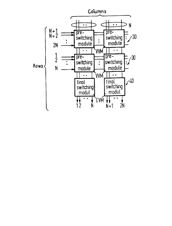
The expansion concept of the modified structure is
illustrated in Fig. 6. The basic unit consists of a pre-
switching and a final switching module. The system can be
expanded in stages of i*N where i = 2, 3 .... In the case of
an expansion from N to 2N, a further basic unit is added to
the basic unit and over this in each case one pre-switching
module. Owing to the structure, an additional outlay of one
module per column is required.
In detail, the present invention encompasses, instead of
r the fully switching expansion module, a pre-switching module
.-, _ _ r w ~-..
2006393
VVM, a pre-switching being carried out only with respect to
the matrix column, but not with respect to the matrix output.
The number of expansion inputs and the number of first outputs
of the pre-switching module is 1/L, namely N, of that of the
expansion module, said module containing a single FIFO store
SP which can read in 2N packets simultaneously and read out
N packets simultaneously. To avoid so-called packet
overtaking, the chronological :.~~quence of packets arriving in
each case on one of the N fir:;t-. input lines of a pre-switching
module is replace~3 from case ~. case by a spatial ordering on
the N first outpu~ Lines of tt,c: nre-switching module WM. The
header informatic~~~ filter KF processes only a part of the
header information for switching the packets to the respective
switching module column. Instead of the basic module, there
are provided in each case a pre-switching module WM and a
final switching module EVM, which carries out a final
switching to the matrix output, the first outputs of the pre-
switching modules VVM being connected to the respective inputs
of the final switching modules EVM. The final switching
modules EVM have no expansion inputs and no expansion outputs.
The header information filter KF of the final switching module
EVM processes another part of the header information for final
switching to a matrix output.
The chronological sequence of packets, which is lost in
the case where packets are read out from the store SP of the
pre-switching module WM in a single packet cycle, is replaced
by spatial ordering in such a way that the packet read into
the store first is output via the first output line having the
highest priority, that is that line which is processed in the
next respective row of the switching network by the store of
.- d~ ~.~i ....~
~OQ6393
the respPCtive switching module as the first of all N
expansion input lines, the second packet is output via the
first output line with the second-highest priority, and so
forth, as a result of which the chronological sequence of the
packets is recovered.
According to a first solution, the spatial ordering is
created by means of a shifting device following the store in
the respective switching moda'e. According to a second
solution, the spatial ordeniv-~ is created by means of a
microprocessor. According t« ;~ third solution, the spatial
order is created by means of ~~ ivl,A (Programmable Logic Array).
The packets ;-riving on '.he input lines with different
packet phases are orought into a common packet phase position
before being proce;;sed in the res~;cctive switching module.
The number of lines between the modules is substantially
reduced from N x L to N. For this, a certain number of
storage locations must be provided in the pre-switching
module, which however are not significant since, in comparison
to the final switching module, the pre-switching module is far
less complex. The results of the comparison are stated in the
table below for N = 16, L = 10 and the expansion stage having
256 lines. The complexity of the filters is reduced by the
factor of 2 in the case of the final switching module and by
the factor of 32 in the case of the pre-switching module. The
complexity of the concentrator and shifter is reduced by the
factor of 2.6 in the case of the final switching module, and
by the factor of 5 in the case of the pre-switching module
(the component width affects the outlay to the power of two).
-,, .P, _ .~ ~ ,-" ,.~, ,.,,
....,~._.-.,.- ... ._ -'~.. ~ --> ._:. ~,i
2oos3s3
KO concept New concept
Expansion Basic Pre-switch- Final
module module ing module module
A.Output 160 1G 16 16
lines N x L N N N
B.Filter 2048 bits 2048 bits 64 bits 1024 bits
C.Concen-26 26 32 16
trator (N-times) (N-time::) (N-times)
width
D.Shifter0 26 32 16
width (N-time:) (N-times)
E.Store 0 S < S/N S
If the indiv.i~ual. modules are constructed in CMOS-VLSI,
then the complexity of the individual module plays an
important role. Namely, in order to be able to keep the
design size of the switching matrix as small as possible, it
is necessary to select the number N of the lines to be
switched per module as large as possible, that is to integrate
highly. The design size is then determined by the complexity
of the circuit which can be integrated on one chip. It is
possible with the present invention described to effectively
reduce the complexity of individual components while
maintaining the same functionality and hence increase the
number of lines which can be switched per module.
In each case the second shifting devices 50 or "shifters
2" in the modules VVM and EVM can be advantageously designed
as multiplexers that activate in each case a selected one of
_.. _ ~. _. :: .._
their outputs.
The invention is not limited to the particular details
of the apparatus depicted and other modifications and
applications are contemplated. Certain other changes may be
made in the above described apparatus without departing from
the true spirit and scope of the invention herein involved.
It is intended, therefore, that the subject matter in the
above depiction shall be interpreted as illustrative and not
in a limiting sense.