Note: Descriptions are shown in the official language in which they were submitted.
~006~~1
Field of the Invention
The present invention relates to systems for
the reception of the power in electromagnetic waves and
conversion of this power to direct current power. More
specifically, it relates to rectenna (rectifying antenna)
arrays which incorporate electromagnetic wave filters and
an optional electromagnetic wave absorbing medium to
reduce the levels of radiated spurious signals.
Background of the Invention
In recent years there have been many studies on
the use of electromagnetic waves for energy transmission
between two separated locations. It has been found in
these studies that there is a need for a cost-effective
means for reception and conversion of electromagnetic
power to direct current power which is suitable for en-
vironments in which the radiated waves from the recep-
tion/conversion system could degrade the performance of
other electronic systems within the range of the recten-
nas. An exemplary application of the reception/conver-
sion system in which this need arises is the provisioning
of 30 KW or more of propulsive and communications payload
power for lightweight electrically-powered aircraft. In
operation, such aircraft would circle over fixed ground
antenna systems, transmitting power in the 2.4 to 2.5 GHz
microwave Industrial, Scientific and Medical (ISM) band,
!2006481
2
for continuous periods of weeks or months at a time, relay
communications signals between separated locations or carry out
other missions, based on long endurance aircraft platforms. It
is, of course, of paramount importance to ensure that radiated
emissions from the rectenna subsystem are not such as to degrade
the performance of payload and aircraft electronics, or other
ground or airborne electronics.
In a previous invention of a dual polarization power
l0 reception and conversion system, a rectenna array configuration
consists of two orthogonally polarized arrays of thin film
rectennas with novel format and particular element spacing.
This system has been demonstrated to be highly efficient for
reception and conversion of the power in a microwave signal
wavefield, received over a wide range of incident angles.
However, it has a significant drawback which may limit its use
in various operating environments, namely its potential for
generating electromagnetic interference. Because of the non-
linear nature of the power conversion process (from the powering
frequency fp to dc) at each rectenna element, a natural by-
product of this conversion is the generation of harmonics nfP of
the powering frequency (where n is an integer). In prior art
200 fi48 1
- 3 -
rectennas, as in the above-mentioned invention and in U.S.
Patent No. 3,434,678, the only measure taken to reduce the
levels of radiation of this harmonic power is the inclusion of a
low-pass filter as a circuit element between each antenna
terminal and non-linear conversion device, such as rectifiers,
etc. When only this means for harmonic attenuation is employed,
significant levels of harmonic radiation, especially at the 2nd,
3rd and 4th harmonics, are produced, as reported in an article
entitled "Environmental Assessment for the Satellite Power
System Conception Development and Evaluation Program -
Electromagnetic Systems Compatibility" by Davis et al, U.S.
Dept. of Energy, DOE/ER-0096, January 1981.
In addition, and of major significance with prior art
rectennas, is the radiation of 'intemodulation product' signals.
In many locations in which rectenna arrays could be used, radio
signals from other users of the spectrum, of a wide variety of
frequencies f~l,...fm, and strengths, will be incident on the
rectenna array along with the power signal at a frequency fP.
2o Non-linear mixing of all received signals at the rectifying
diode will result in the generation of spurious intermodulation
signals at combination frequencies ~kfp~EIn
n
;..
200~~4~1
' 4
Due to the high level of the powering signal, these in-
termodulation product signals will be radiated at suffi-
cient amplitudes to interfere with the performance of
other electronic systems. The only measure taken to
reduce this radiation in the prior art rectennas is the
previously-mentioned low-pass circuit filtering which,
because of the severity of the problem, in many circum-
stances may be insufficient to reduce the level of inter-
modulation product signals sufficiently to comply with
regulatory standards set for interference levels.
Summary of the Invention
As will be discussed in detail below, the
aforementioned deficiencies of the prior art systems are
significantly reduced with the present invention. Brief-
ly stated, a low noise dual polarization electromagnetic
power reception and conversion system according to the
present invention consists of a plurality of frequency
bandpass filter elements arranged symmetrically in an
array in a first plane for spatial bandpass filtering an
incident electromagnetic powering beam and incident am-
bient signals. The system further includes a plurality
of antenna units, each having a power conversion cir-
cuitry, arranged symmetrically in an array in at least
one second plane behind the first plane for receiving in
dual polarization and converting the powering beam and
~os481
for non-linearly mixing the ambient signals and the
powering beam. A plurality of frequency bandstop ele-
ments are arranged symmetrically in an array in a third
plane behind the second plane for bandstopping the power-
s ing beam and the ambient signals.
Objects of the Invention
It is an object of the present invention to
provide a high efficiency power reception and conversion
system with characteristics such as to minimize the
levels of spurious signals radiated at harmonics of the
powering signal frequency.
It is a further object of the present invention
to provide a high efficiency power reception and conver-
sion system with characteristics such as to minimize the
levels of radiated spurious intermodulation signals re-
sulting from the nonlinear mixing of the powering and
communications signals incident on the rectenna.
It is a further object of the present invention
to provide a high efficiency power reception and conver-
sion system capable of operating efficiently over a wide
range of angles as may be required to accomodate varia-
tions in angular orientation of the rectenna system rela-
tive to the direction of the incident electromagnetic
powering signal wavefield.
20Q~4$1
6
Brief Description of the Drawings
Other objects, features and advantages of the
present invention will be apparent from the following
description taken in connection with the accompanying
drawings, wherein:
Figure 1 is a perspective view of the present
invention according to one embodiment comprising two sur-
faces of conducting elements with, in between them, an
array of antennas and associated conversion circuits, the
ensemble followed by a layer of absorbtive material.
Figure 2a is a schematic transmission line net-
work model representing the power transmission and recep-
tion process for one polarization of the power beam.
Figure 2b is a schematic transmission line net-
work model representing the generation and control of
harmonic frequency radiation for one polarization of the
rectenna unit.
Figure 2c is a schematic transmission line net-
work model representing the generation and control of
intermodulation product frequency radiation for one
polarization of the rectenna unit.
Detailed Description of Preferred
Embodiments of the Invention
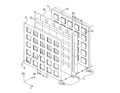
Figure 1 illustrates a low noise power recep-
tion and conversion system configured according to one
embodiment of the present invention. The power reception
~0~~481
7
and conversion system 1 is positioned to intercept a
portion of an electromagnetic power beam 3 transmitted in
a direction z perpendicular to the x-y plane of the ele-
ments, as shown by the coordinate system in the figure.
The remote transmit antenna emits dual polarized waves,
that is, waves of two orthogonal polarizations, which
could be unequal in amplitude and phase. These two or-
thogonal field components of the incident beam can be
resolved into components aligned along each of the two
directions x and y, respectively, of the power reception
and conversion system 1.
These field components are incident on a fre-
quency selective surface (FSS1) 5, located at a first
plane. Such surfaces are known in the art and perform
the electromagnetic wave equivalent of circuit filter
elements. Further discussion on such surfaces is found
in Applied Optics, Vol. 14, No. 2, pp. 217-220, "Equiva-
lent-circuit formulas for metal grid reflectors at a di-
electric boundary" by Whitburn et al. Therefore, they
perform low pass, high pass, bandpass, etc., spatial fil-
tering functions, depending upon their specific design.
The frequency selective surface 5 shown in Fig. 1 is a
bandpass filter capable of transmitting only frequencies
over a narrow band including the powering frequency fp.
In this embodiment, the surface is a metalized or metal
20~~4~1
8
meshed plate or the like, with an array of openings 7 whose
sizes and locations are mainly determined by the frequency and
the antenna units used.
Ideally, only the powering frequency is passed with no
attenuation, but in practice, the design of the filter is chosen
to optimize its electrical characteristics of attenuation inside
and outside the passband and bandwidth, for each specific
application. Typically, frequency selective surfaces attenuate
~30 dB in the stopband and less than 0.5 dB in the passband.
The filtered incident powering beam then travels a
distance q to the antenna array 9 located in two second planes
10 and 12 (foreplane 1 and foreplane 2 respectively) where the
usual rectenna functions of power reception and conversion take
place. This antenna array, for example, can be of the type in
the previous invention noted earlier. In this embodiment, the
rectenna arrays are provided in two parallel second planes one
for either of the two polarizations separated from one another
by a predetermined optimum distance, e.g. nl~o/2. It is, of
course, possible to provide a dual polarization array antenna in
only one second plane.
The unreceived portion of the powering beam
travels to the second frequency selective surface (FSSZ)
t
2~~1~4~1
9
11. This surface is a bandstop spatial filter, reflect-
ing only frequencies around fp and is located in a third
plane at a distance p behind the nearest second plane.
This surface reflects the powering beam and other signals
of the same frequency in the correct phase back to the
rectenna to improve its reception efficiency in an analo-
gous fashion to the normal rectenna reflector plane.
Also compensation for the effect of rectenna transmission
lines is achieved by a specific choice of dimension p.
The bandstop filter shown in the figure is the complemen-
tary structure of the mesh or metalized bandpass filter
also shown in the figure. It is made of square disks 13
of metal arranged in an array and supported by a thin
transparent film. For the powering beam of 2.45 GHz in
the ISM band, typical dimensions a and g shown in Figure
1 are a = 0.6 cm and g = 12 cm.
A layer 14 of lossy material may be provided
behind the third plane. Although for clarity only one
surface is shown for each filter, several surfaces may be
used for each filter function equivalent to multi-section
circuit filters, to improve the filter's performance, by
decreasing the level of power transmission or reflection
of wavefields on frequencies outside the passbands or
stopbands.
2006481
to
Figure 2a shows the equivalent circuit of the
system in the manner described in "Far-Infrared Proper-
ties of Metallic Mesh and its Complementary Structure" by
Ulrich, Infrared Physics, Vol. 7, pp. 37-55, Pergamon
Press Ltd., 1967.
The two second planes are designated by 21 and
23. Free space impedance and wavelength are Zo and
The frequency selective surfaces on the first and third
planes are shown by FSS1 and FSS2, each consisting of Llo
and Clo and L2o and CZO, respectively. The equivalent
circuit parameters for these filters are determined by
the dimensions of the openings and disks and the design
bandpass or bandstop frequency. These parameters in turn
determine the in-band and out-of-band characteristics of
the filters.
The behaviour of the present invention at the
powering frequency fp will become clear upon examination
of a network model for one polarization of the incident
beam of Figure 1, as it passes through the system. This
model is shown in Figure 2a. This transmission line
equivalent circuit is based upon the unit cell concept
used for the quantitative analysis of large arrays and
associated elements. When the frequency selective sur-
faces are designed with the same symmetry and periodicity
properties as the antenna units, the unit cell concept
2t~~~~~1
m
may be used for understanding the behaviour of the en-
semble of elements. From this network model it is evi-
dent that, for the powering frequency fp, no losses occur
at either the first or second frequency selective surface
and that high efficiency of reception of the powering
beam by the rectenna units is possible. This is ensured
by the choice of circuit elements L10, Cio of FSSl and
L2o~ C20 of FSS2 at the powering frequency such that
2 - 1 1
L10C10 ( )
lU and f 2 = 1 (2)
L20C20
The above explanation has considered the case
of a powering beam normally incident upon the system,
however, this high efficiency of power reception is pos-
Bible at any specified angle of incidence, upon modifica-
tion of the transmission line (unit cell) parameters Zo,
in Figure 2a. Furthermore, these frequency selective
surfaces can be made relatively insensitive to deviations
from the designed angle of beam incidence, and may thus
be used in cases where the range of beam incidence angles
cannot be carefully limited. For more detailed descrip-
tion of this aspect, reference can be made to an article
entitled "Equivalent-circuit models for frequency-selec-
tive surfaces at oblique angles of incidence" by Lee et
zp~~4~1
12
al, IEE Proceedings, Vol. 132, Pt. H, No. 6, pp. 395-399,
October 1985.
From the above discussion, by referring to
Figure 2b, the behaviour of the system at harmonic fre-
quencies nfp may be readily visualized, with the assis-
tance of a network model for the system at the harmonic
frequency of interest. It is to be noted that for both
harmonic and higher frequency intermodulation product
generation, the frequency of these generated signals will
cause more than one transmission line mode to be of sig-
nificance. Each of these modes corresponds to radiation
(of harmonics or intermodulation products) in a specif is
direction in space. This condition is represented by
paralleled transmission lines in Figures 2b and 2c in
which two such modes are illustrated. In these figures,
like designations are used for like elements and para-
meters. An optional layer 25 of a lossy material is also
included.
Signals on harmonic frequencies and other fre-
quencies out of the system passband, generated at the
rectenna diodes, are prevented from radiating into free
space by frequency selective surface FSS1. Instead, they
are reflected by FSSl back towards the rectenna and then
propagate through FSS2 after which they are absorbed by
2~OE~81
13
the lossy material behind this filter. In certain ap-
plications of this invention (for example the powering of
an aircraft from the ground, if there are no sensitive
electronic components on the aircraft or nearby which
could be affected adversely by these harmonic and other
signals), the lossy material above FSS2 may not be neces-
sary, and construction materials could be chosen to allow
harmonic and other signals to propagate into the upper
atmosphere and space (above the aircraft).
From the preceding descriptions, the behaviour
of the system for spurious signals at intermodulation
product frequencies ~kfp~lf~ may be understood, using the
network model of Figure 2c.
In the case where the frequency of the ambient
signal, f~, is outside the passband of FSS1 (centered on
fp, no intermodulation products will be generated. In
the case where f~ is within the passband of FSS1, inter-
modulation products will be generated, but unless the
frequencies of these products fall within the fp pass-
band, they will be prevented from radiating into space
and will be absorbed in the layer behind FSS2.
The above described invention will reduce the
level of all radiated harmonics and intermodulation pro-
ducts (outside the passband of the invention). Further
attenuation of one harmonic or intermodulation product is
20~?~~81
14
possible by the correct choice of distance q, between
FSSl and rectenna foreplane 1. For example, minimization
of the second harmonic (often a desirable objective) in
the broadside direction (the lower transmission line mode
of Figure 2b) will occur for the 'shorted' (at 2fp band-
pass filter when placed approximately X0/4 from the rec-
tenna foreplane l, effectively 'shorting' the rectenna
source at the second harmonic.