Note: Descriptions are shown in the official language in which they were submitted.
15~2d Inven~ors: John M. I~w~ ZO~ 5
-l 523d Joseph Da~3"pc~r~r
I~SPROV~D Ml~T~O~) ~FOR ~Il~G PRIN~EI) CIRCIJITB
BA~ o~l~!~
This inv~n~ion is rela~ed to printed circuits for
use in electrical and el~ tronic equipment. In
parti~:ular, it is an improved method o:~ making
prin-ted-circ:~lit ~oards and of p.roduc:ing printed
circults vn ~urfac~s o~her than conven~ional
printed-circllit boards. This inven~ion is also
concerned with malcin~ printed circ:uits ~nd is
especially con~erned With a me~.hod of making a printed
Ci~llit ir~ which ~ l~Lyer iS applied in a desired
pattern to a s~strate~
P~n element th~ ls co~anon to alJnost all electronic
equipment i5 t~le printed çir¢uit, typic~ally in the ~orm
OI a printPd-circ~uit ~oard ~PCl~)~ A PCE~ is gener~lly
made by laminating copper foil to a }~oa~d. A d~sired
pat~ern that in(;:lu~le~ c:onduc:~ors in the plane o~ ~t
- least ~ne sur~aC~e of the board is plac:ed upon the
~oard, and h~les are driIled or punched for the
mo~nting o$ components. ~his pa~tern is t~pically
realizçd ~r plac~ing a photos~nsitive res~st on the
board, expo~ing a photos~raph of the de~ired pattern on
~he resi~t, and developi~g the re~is ~o produ~.e a
protecti~e c:oa~ing ove~ th~ pa~tern. The remainder of
2(3~ 8~
,~
the resist i~ treated to remove undeveloped resist from
p~rtion3 where it i5 desired to remove th~ copper. The
board i~ then treated with ~ process ~hat removes the
expossd copper. When ~he rem~ining resist is then
re~oved, the desired pattern remains in the copper.
Mounting holes for components are drilled or punched at
desired lo~a~ions som~whers in the course of this
proce~s, either before or after the removal step.
The ~aterials most comm~nly used for PCBs are
0 either polymeri~ed epoxy ma~erials containing glass
fibers or paper b~und by imp~egna~ed syn~hetic resins
such ~ phenolia mate~als. The la~te~ group is of~en
rcfer~ed to generically a~ syn~hetic-resin-borlded paper
(SRBP). Boa~ds made o ei~her of ~hese types of
materials are clad with copper on one side or both
sidesl w~th ~he heat and pr~ssure of the cladding or
laminating proce~s helping to cure the resin. The
ma~erial cost of an S~BP PCB i~ typically about hal~ as
much as that of an epoxy fib~glass ~ard of the same
surfa~e area, ~o th~re is a po~enti~l co~t advan~ge
when the SRBP b~rd can be used. There are various
bases for ~he selection b~tween epoxy fiberglass and
SRBP m~terial~ For example~ the ep~xy fiberglass
~o~rds are ~ene~ally higher in strength ~nd are
preferred for use in equip~ent ~h~t may be subje~t ~o
vibra~ion.
A particular probl~m ~f cirouit design tha~ leads
to complica~ion in P~Bs is ~he ~at ~ha~ not all
electroni~ circui~ can be m~de wi~h their conne~ions
3~ in a single plane. I~ is sometimes necessary to make
~ridging ~onnections between different portions of a
circuit, A considerable amoun~ of ingenui~y goes into
~he design and layou~ o~ PC~s to ~inimize suc~ bridging
connection~ How~ver, ~ome~imes i~ is impossible to
3~ a~oid ~hem~ In suGh ~ ca e, it i~ possible ~o solder
,, ,
s~
- 3-
-jumpe~ wires bet~een the portions of ~he circuit th~t
are to be connect~d. mis 1~ ~specially undesir~ble
for long runs, and it is b~tter avoided ev~n for short
r~n~. A better s~lution i~ to use PCBs that have more
than one condu~ting layer. Tha ~implest of these is a
two-sided PCB. ~his i~ a hoard that has copper
.la~inated to both sid~s. Separat~ patterns ~re etched
on the two ~ides to ePf~t t~ desired circui-t layou~
and cxoss-conne~tion~. How~er, in order to make such
cros~-connections, and to ~o~plete the ~onnection
be~ween the two si~e~ o~ ~he ~oard, it is normally
necessary to use ep~xy fiberglas~ because of ~he
ne~essity of pl~ting ~oles ~rough the board to connect
the top layer ~o th~ bott~m~layer. Holes that are
drilled in an SRBP board are adequate to support the
l~ads of components ~h~t a~e placed in the ~oard for
sol~ering, but the~ are no~ normally clean enough when
drilled or ~unched to p~rmi~ ~atis~actor~
eleotroplating o~ ¢onnections between layers of the
board, There is thu a l~ng-felt need in the PCB
industry for a way o~ ma~ing PC~s with cr~sso~er
connections on single-sided SRBP boards without using
: solde~ed jump~r wir~s.
The ~a~e con~iderations apply equally as m~ch to
boards ha~ing ~ore than two layers. These boa~ds,
referred ~o ~9 multil~yer boards, are often used in
more complic~ted ~ir~uits where ~ne set of br~dging
connections is not ehough~ ~ with ~he two-sided
~o~rd, it is normally necessaty to use epoxy fiber~lass
for such P~B~ It ~an be s~n th~t the result of a
need fo~ ~rossed csnn~ ns in the typical etched
copper PCB l~ds to an incxea~e~ ~05~ beca~se of the
need ~or epoxy ~iberglass ~n the P~ inste~d of the
less-e~p~nsive SRBP boards~
~he problem~ ~s~ de~cribed beco~e extr~me in the
-- 47
case of PCBs for X~yboards. A Xeyboard for a
typewriter, compu~ or the like typically generates an
ele~txical ~ign~l when a key is depressed to make an
electrical ~ont~ct or ~n induative or capacitive
coupling. Su~h a coupling ~s made dir~ctly or
indirectly between two sep~rated conductors on the
boar~ or on a flex.lble pl~sti~ me~br~ne that is spaced
ap~rt from the board and make~ a condu~tive or field
contdct when pre~se~ ~oward the ~oa~d. Wh~n the
1~ k~ey~oard is ~he typical typewri~er or computer
ke~boar~, it i~ impo.~sible or nearly impossible to
~oid crossed connections. The physical size of the
hands of an operator also set~ a limit to the minimum
size of a P~B for a keyboard, ~inc~ it is necess~ry to
place a keyboard swit~h on th~ P~B at a location
dire~ly beneath the key t~ ~e ~epressed. As a result,
~he typical PC~ for a keyboard i~ of -the order of ten
to eighteen inches by four to seven inches (25-45 cm.
~y 10-18 cm.~ This s~ze requirement h~s caused the
PCB to beco~e a significant pa~t of the cost of a
~ypew~i~er or comp~er k~yboard. It is not normally
possible to us~ an SRBP P~ because o~ the need ~or
cros~overs.and the at~endan~ plated connecting holes.
~he re~ult is a rela~ively expe~ive epoxy fiberglass
~5 PCB, lamina~ed and etched on hoth sides. ~his cost
could be gre~tly r~du~d i~ it were possible to use an
SRBP ~oard ~ha~ contained a ~cuit on only on~ side.
A s~cond pr~blem in th~ manufactu~e of PCBs for
keyboards is the f~ct ~hat Xeyboards either have pairs
of exposed elea~ric~ ondua~ors th~ ~re ~ridged hy
~nother conductor or coupled cap~ci~ively or
inducti~ely to make an elec~rical ~onne~ion when a key
is depresse~, o~ el~e ha~ flexi~le membranes that
~o~pl~ ~o the board wh~n pr~sed. It is necessary to
apply ~ome f~-rm o~ pro~ection to the exposed electrical
. ~
-- 5--
condu~tor ~o a~ to ~inimize the buildup of corrosion
that would interfere with t~e malcing of the electri~al
conn~ction~ This is mo~ com~only done by etchinq a
copper p~ttern o~ interlac~d com~s, parallel conductors
or the like ~nd plating ~ld to the oombs to provide a
cont~c~ surfac~ that i~ conductive electrically and
that is not readily aorroded ~y exposure to the
atmosphere. Gold m~y b~ plated ~o the copper either by
electroplating or by ele~roless plating. Either of
these represents an add!itio~al element that contributes
to thR cost of prep~ring a PCB for a ~eyboard.
The usual intende~ use Qf a PCB is to se~ve as a
mount for compon~nts ~uch a~ resistors, capacitors,
diodes and transis~or~. Any ~ these components is
lS ~ypic~lly inser~ed by pla~ing i~s ~eads into holes in
the PCB whic~ is then p~ssed through a wave-soldering
process to at~ch the components physically and
electri~ally to ~he P~B. Durin~ the process of
manufacturing ~he PCB, the b~ar~ is typically coated in
part with ~n organic polymer solder resist to prevent
solder f~om adheri.~ to:tAhe ~ove~ed regio~s. If the
PC~ is one de~igned for a keyboard, the resist is
typically depo~ited so ~ to cover conductors on the
~eyboard surfa~e but i~ ~a~ked ~ leave the com~ or
other keyboard s~it~hes exposed fo~ opera~io~,
A USQ tha~ is analog~us to that of P~Bs is the
manuf~cture o~ electrical c~hlQs or the like by
deposi~ing aonduc~ing mate~i~1 on flexi~le plastiçs
su~h as mylar. ~rhis is o~en ~one by some fo~m of
printing p~cess such as screen print}ng . Mos~, if
not all, of the ~akerials, typically plasti~s, th~ are
used for flexi~le cables or flexible ~la~ ~onduc-~ors
are no~ ad~pted ~or wa~-sol~erin~, and i~ is the~efore
necessary to make co~pression conne~tions or ~he like
at the ends of th~ c~bl~ or flat conductor. As a
3~ 5
- 6~
r sul~, ther~ is no w~y to a~ach resistors or
cap~citox~ to flexible material, and a rigid Pc~ is
thereore used with the flexible material to serve as a
componenk ~ount.
STJM ~ ~O,F ~HE I ~ I QN
It is an object of ~e present invention to
pro~ide an al~ernative method of making electrical
irlterconn~ctions.
It i~ a furth~r object o~ the pres2nt inven~ion to
provide a be~ter wa~ of making printed circuits.
It is a fur~her ob~ect of the presen~ invention to
provide a be~ter way of ma~ing printe~-cir~uit boards
It i~ a fur~her o~ec~-o~ the presen~ invention to
~S pro~ide a ~thod of ~aking 4ros~ed elec~rical
connections on a ~ingle side of printed-circuit board.
Xt is a further o~ect o~ the pr~en~ invention to
provide a ~thod of producing resistors by a printing
process on the prin~ed-cira~i~ board.
It is a further ob~e~ ofi the present invention to
provide a method o producing capacitors by a printin~
process on a printed-~ircu~t ~o~rd.
It is a f~rther object o~ the pres~nt inven~ion to
provide a method of pr~ducing a printed ~ircuit on
: 25 ~exible ~ubstrate.
I~ is a fur~her object of the p~esent invention to
produce ~ p~inted circuit inclu~iny resis~ors ahd
capaci~or6 on a subs~ntialIy planar solid sur~ace,
It i~ ~ further ob~t o~ ~he present inYention ~0
produce a printed cir~uit in~l~ding resistors ~n~
capacitors on a c~rved surfa¢e.
It i~ ~ further objec~ of ~h~ pre~ent invention to
enable ~he use of synthe~ic-resin-bonded p~per
: printed-cir~uit boards by e~ectiny multilayer printing
on one side o~ the ho~rd.
~ , ~
~ 8'3
Other objects will become app~rent in th~ course of a
detailed de~ription of ~he lnvention,
Print~d circuit~ are produce~ by screen printing
or the like to deposit conductors, resistors,
cap~citors and insul~tors. crossover connections are
made by covering the ~onducting portions to be crossed
with an in~ulat~ng ~te~lal t~ serves as ~ base for a
print~d crossing aonductor. Exposed conductors, as for
keyboards ~nd compresslon connectiorls, are pro~ected
lo fro~ the development o~ high-resistance co~rosion
product~ by printing or ove~printing them with an ink
that deposit~ ~ car~on layer. The method pe~mits the
use of rigid prin~ed-circuit bo~rds ha~ihg crossed
connections without requiring the use o~ a ~wo-sided
ho~rd. The equiv~lent of ~ultilayer boa~ds can be
achieved by printing repe~t~d layers of conductors,
compon~nts and ins~lators on the same side of the
board, or ~y printing on two~sides of a board.
Interconnection b~tween adjacent layers can ~e made as
a part of the printing pxo~ess~ Resistors c~n be
printed by screening or otherwise depositing a
controlled amoun~ of a resistive ink. Cap~citors can
be produced by print~ng cond~ctive layers separated by
insulating lay~rs. ~he p~OC2~ ~ay produce
printed~circu~t board~ con~ining resistors and
cap~citors wi~hout th~ neG~si~y for inserting and
wave-soldering co~ponents. If such ~ board is to
~ontain components i~ addition ~o those printed by the
process of ~he preqen~ invention, a prin~ed carbon
layer can be u~ed ~ old~r re~is~ to proteot printed
condu~ors ~uring ~he w~ve-soldering proces$, ~n~ ~o
p~o~ect exp~sed conta~s, ~s for key~oards, duriny
wave-solder~n~ and in use~. ~he p~ocess alao permits
the printing o~ a conduoting Iayer ~s a shield against
3~ radio-frequ~ncy in~erference or a~ a ground plane to
x~çj~s
provide electrical isolation of por~jon~ of a circuit
from e~ch other.
A mQthod in accor~ance wi~h the invention permits
production of a printed ci~cuit on a flexible
substrate. Resistor6, capa~i~ors, ~onductors and
insulator~ may be produ~d on a substan~ially planar
solid surface or on a ~urved ~urface~
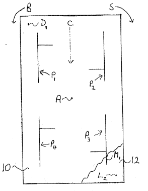
BRIEF I~ESC~I~:[O~oF ~: D~AWINGS
Fig. 1 is a diagramma~ic plan view of a ~creen
wi~h a corner broken away revealing a substr~te above
which ~he screen is positioned, in a position for
~pplying a first coating; and
Fig. 2 i~ a ~lmilar pIan ~iew showing the sc~een
and subs~r~e in po~ition for applying a second coating.
.
D~TaL~ED DE$~IP~ION ~F ~H~ ~VENTION
The examples ~h~t ~ollow ~epresent particular
applications of the in~ntion. In the case of those
applications t~ ~eybo~rds for -~ypewriters or computers
or the like, the s~alR is ~ix~d ~y the size of the
hand~ of an operator, ~nd the re~ ing necessity ~o
sep~rate ~he keys physica~ly. ~hese dimens~ons fix the
~5 size of ~uch a ~ircuit ~o~rd~ So~e of ~he ex~mples
r~la~e to ~onven~ional printed-~ircuit boards in which
~ co~ponents will ~e ~nserted and wave-sold~red. The
: po~ibility of limiting $he printin~ to one side of a
board also makes it possible to print a oircuit on any
~face on which it ~an ke.printed ~nd on any ~ubst~nce
~hat is compatible wit~ the printin~ process. Thus,
the pl~5tiC of a ~ar dashbo~d, tXe aase of a radio, a
flexible pl~stic or pap~r transfer medium, or a he~t
si~k could be ~s~d a~ a substrate on which to print
cir~uit according So th~ pre~ n~ inven~ion. Th~
,
.~ ,
:'
.
20~3f;~ ~5
_ g_
exa~ples shown her~ were ~lso pro~uced by a screen
printing process, whic~ repre~en~s a preferred method,
but it i~ clear that any ~ethod of printing th~t will
h~ndle the conduc~ing, re~istive, carbon and
solder-resist inks wil~ be adaptable for the present
p~ocess ~nd for pr~ducts produced by the process. The
other possib~lities for doing this include transfer
p~inting, li~hography, air bru~h, hand brush, and the
like. ThP exampleS that ~ncluded ~he printing of
resisto~s and c~pacitors produced such components
having valu~s th~t were repeatable within tolerance
ran~es of ~i~e to ten per ce.nt. These values are thus
compar~ble to t~ose achie~ed with ~rdinary discre~e
component~
~xam~
An SRBP board a~roxim~tely 14 in~.he.~ by 4 inchQs
by 11l6 inch co~tained ~ lamina~ed layer o~ copper that
had been etc~ed to pr~duçe condu~ting pat~s and
2~ appr~priately placed co~b connectors to be bridg~d by
conducting pills when a key was depressed. The combs
were pl~ed with gold. In order to function properly,
this b~arA needed connectivns ~hat would cross ~ertain
conducto~s without m~king electrical contact with
them, The cros~lng connec~ions were achieved by screen
printing with an ink containing a pol~er resis~ at the
crossings. ~he resi~ was cured using ul~raviolet
~diation. A ~onduct~g path connecting ~he desired
po nts w~s then prin~ed ~y a sc~een process over the
cu~ed resist,: ~nd ~he prin~ed condu~tor was then cured
at an ~leYat~d ~emperztur~ This produced a
functioning printed ~ircuit bo~d ~or a keyboard that
was printed. ~n only one sid~ of the PC~ and that had no
~idgin~ wixe conn~ctions.
3~ .
-- 10--
xAamPl~, ~
An S~P board approximately 14 inches ~y 7 in~hes
by lJ16 inch had bflen lamln~ed with copper and the
copp~r had been etched to leave an ~pprop~iate pattern
of electri~l connect~on~ ~or a keyboard. Thi5 pattern
was placed on a single ~ide of the phenolic board.
Each of the contact pad~ ~or ~he keys was formed by a
~creen p~lnting o~ a c~nd~c~ive in~. This ink was then
cu~ed by heati~g. The ~ontact pads ahd also ~xposed
condu~tors for c~mpr~sion conne~tors ~t an e~ge of the
~o~rd were then covered by screen printing with an ink
containin~ car~on, and the ink was cured by h~ting
it. A screen printing was ~hen made to apply an
insulating polymer r~ist ~o all areas of ~he board
except the exposed conductor~ f or the key pads and f or
compresslon conneatiOnS at ~n edge of ~he board and at
~hose areas where ~omponent~ we~e ~o be inser~ed and
wave-soldered. ~he cured: ~arbon ink functioned as a
s~lder resi~ that pro~ected the contac~ pads ~rom
solder du~ing the wave-~oldering process. If the board
had been subjected to hand so~dering, the carbon ink
would have proteoted the contact pads from damage by
hea~.
E~B~
A keyboard o~ FR-4 epoxy ~be~glass having
di~ensions o~ approx~ately 14 inch s by 7 inches by
1/~6 inch h~d ~een lamlnat~d and ~tahed on one side to
le~ve copper conducto~ in a pa~ern appropriate for a
keyboard. Layers of insulating resist were screened in
desired ¢rossover pa~erns on the sid~ of the b~ard
that carr~ed ~he aopp~r ~nd we~e cured by ultraviolet
r~dia~ion. A ssreen print~ng was then maae ~ith a
conducting ink ~o apply aonducting strips on the
aro~30vers and al~o print ~h~ contac~ ~eas for keys.
3~
. ., -- 11--
q'his was cured by heatlngO The area~ of screened
cond~ctors were th~n subjected to a further screening
proce~s to cover the screened conductors with ink
containing car~on. Thi~ was then ~ured by heat. ~he
bo~rd Was then equipped ~ith resistors by screen
printing with re~iYtiv~ ink in desired locations.
After the printed resis~o~s were cured by heat, ~
protective layer of solder resist was applied and was
then cured by ultr~violet r~diation. 'r~e solder resist
l~ft open areas for the applic~ion of solder. Because
of the carbon ~verin~, ~his board could be subjected
to flow solderin~ without damaglng ~he screened
connec~rs and co~ponen~3.
'
Ex~mple ~
An SRBP board approxima~ely 1 inch by 2 inc~es by
1/16 in¢h had ~een lamina~ed wi~h copper foil on one
side, and ~he foil w~s etched t~ leave a desired
ci~cuit pat~ern. A porti~n of the board was COvered
zo with a ~c~eened ~sis~ which was then ~ured by
ultraviolet light. A conduc~ing ink wa~ pxinted by a
s~reen proce~s over the r~ist to make a conducting
crossove~. The Gondu~ing ink ~as als~ placed over ~n
~rea app~ximateiy 1~4 ~n~h square to fo~m one pla~e of
~ capacitor. ~he condu~ting ink was ~ured hy heate
R~sistor~ were dep~si~ed in de~ired locations by
screening resistivè ink which was then cured by heat.
A layer o~ re~ist w~ ~epo~ d over the ~ond~c~ing
area ~o pr~vide a dielectric material for ~he
c~pa~itor. Thi~ wa ~h~n cured by expo~ure to
u~tr~iolet light. A se¢ond con~u~ting layer was
printed by screening to cover the re~is~ and form the
second plate of ~he capa~it~r ~nd al~o to connect ~he
capacitor ~t a d~ired poi~t:on ~he aopper lami~ation,
and t~e ~nduc~in~ ink waæ aured by heati~g i~. ~he
- 12- X~3~
~e~ult wa~ a circuit board wi~h connections and
component~, A prot~¢~ive layer of solder ~e5ist waC
appli~d with hole~ for ~older points, and the re5ist
was ~ured by ultraviolet radia~ion.
~x~elç 5
An S~BP board ~f dimen~ion~ approximately 2 inch0s
~y 1 inch by l/l~ inch x~ceivRd a s~reened pattern o~
condu~ting ink which ~as th~n cured by ~eat. A pattern
of æcreen reæist~ve inks w~ p~a~ed by a sare~n
printin~ pro~ess ~n desired l~cations, and -~he
re~istive ink wa~ cure~ by heat. 5ele ted locations of
the sc~eened conductor weXe then plated with ~oppe~ in
an elec~roleæs platlng tanX, A pro~ective resist was
th~n screened over all ~Ut:thO~e portions of the board
that were to he exposed ~or ~ontact~ This includqd the
area~ that wPre ~i~sn the copp~r plate, which readied
that r~gion o~ the b~rd for sold~red cont~ct, ei~her
manual or automati~ soldering. As an alternative,
nickel coul~ equally aæ well h~ve been plated ~o
; provide an appropri~e sol~ering su~face. The
conducto~s formed by ~onducting ink w~ll not generally
wiShstand the heat ~sso~la~ed with hand ~oldering,
althouyh ~hey may stand up under wave-soldering.
~ : .
A~ SRBP board 1~ inch~ by 7 in~hes by l/16 ~nch
wa~ scraen-prin~ed wi~ a condu~ing ink in ~ patte~n
appropria~ k~yboard. Th~ ink was ~ured by heat,
and crossing aonn~cto~s were p~c~d by the procçss
~escribed akove. Registive ink in ~on~rolled pa~terns
was prlnted and ~ured by heat ~o produce desired
resi~tor~ as de~ribed abov~. A layer of solder resist
w~ then sc~eened on the board in a pat~ern tha~ left
: 35 suhs~antially sq~are openings at the loc~tions of the
~' ' . '
,
13-
typewrite~ keys. Th~ re~ist w~s cu~ed b~ exposure ~o
ult~aviolet light~ Th~ cured resist served as a
mechanic~l ~pacer .~o~ a ~embr~ne wi~h appropriately
pla~ed aonductors tha~ was laid over the resist. ~his
provided a m~thod Qf ~aking a membrane-~witChed
keyboard without the neces~i~y of tooling to cut
open.ing~ in a pieae of pla~tic to space the membrane
fro~ its ma~ing ~leatric~l conneation. The connections
made he~e w~r~ capacitive, but they could e~ually as
well have ~een ~onduati~e oX inductive. The process
could also have been applied to make ~witches using two
parallel membranes that were spaced apart ~y screened
and cured resist rather thah using a rigad board as one
connector support.
All of the board~ des~ribed in the examples above
have in co~m~n the fa~ that all of ~heir printin~ is
done on one side o ~he board. Some boards have been
made in ~he pas~ wit~ j~mper wires that ~re
wave 301der~d as a part of~the process o~ makiny the
board, bUt this i3 seldom a go~d solution to the
problem of bri~gi~g connectorY and i~ is often
unfeas~le if the run of condu~t~rs to be hrid~ed is of
any length~ Another problem that can be overcome much
mo~e simply than ths presen~ prac~ice is that of
providing sh~elding against ~ad;o-~r~quency
interference ~RFI shieldi~g). One reason for the use
o~ multilayer boards is to pl~co a shieldin~ layer
pro~ecting po~tionS of ~he circui~. ~his is done much
~ore simply ~n a single la~er boaxd on one side by
depo~iting and curing ~ ~ondu~ing layer oYer a layer
D$ re i~t.
~h~ pro~ess o the pre~en~ inven~ion is adaptable
to prin~ as many ~ thirt~ ~o ~ifty layers, one on top
of the o~her. The prac~ical minimum spacing b~tween
3~ adjacent co~du~or~ f the order of O.ol inch. A
- 14- ~n~i~8~
screened layer ~fter curing c~n typically be controlled
in thickne~s ~o plu~ ox min~s 5 microns. ~pacitors of
variou6 value~ ranging 4p to 1000 pico~arads may be
made as de~cribed in th~ examples, wi~h tolerances to
S per cent.
In som~ ci~cums~ance~, plnholes in one of the
applied layers may aause probl~ms, espeCia~ly in an
insulation ~ayer wh~re p~Jihole~ may cause unintentional
: ~nd c~ta~trophia connection betwe~n conducting layers.
In order to reduce the risks of this problem ~rising,
the or each in~ulat~ng layer may be applied in two
: ~tages, so tha~ two coating~ a~e ~pplied ~ith ~riation
of coating direction or slightly p~sitional vari~tion
between ~he coatin~s~ For example, when applying an
15 insulating layer usin~ s~reen printing t~e first stage
comprises applying a ~reened co~ing with the
dire~ion of appllcation a~ong the X-axis of the screen
and work-piece. Th~ sec~nd ~tage a~mprises applying a
further screened coatinq w~t~ riation from the
20 ori~in~l co~ing, for example ~ er by rotating both
the screen and the work-piece t~rough ~0, rel~tive to
the coating direG~ion, and/o~ with the s~reen offset
relative to tne work-piece, e.g. in the X ~ndJor Y
direction, by a m~ni~al a~un~ e.g~ ~ small part of a
25 millimetre.
T~e Table i~ a lis~ln~ of the inks th~t wPre used
in a screen printing process ~o produce ~h~ examples
above.
~0 ., :
,
'
. .
:
. ' ' , .
- 15~
__________~_______._~________~;_ __ _________________
Tl!~BLE
SCREE~ PRINTIN~: P~OC~ESS I~KS
. ~ç~ ni~ ~ a cro~-linking polymer
sold under ~he ~radem~r~ "Phot.o~o~t.
The exa~ple~ u~ed type ~G which i~ n~
flexible, al~h~ugh a style 3G is
availablQ t~t i~ ~lexible. The
examples u~ed a re~ that was curable
by ultraYiol8t r~d iation~ . A
heat~curable re~ could equally as
wel~ h~e ~e~n u~ed.
2Q
2. ~esi~tiv~ ~nk. All~o~ the examples used
a polymer thick-film ink ~old under the
trade n~me 'IM~tth~y L~" R-4000 series.
~his is a~aila~le in a r~nge of
resis~ivl~ies ~nd ls cured by hea~.
3 Ç~n_ln~ T~ i5 a~p~lymer
thick-fil~ lnk con~aining c~rbon black.
It i~ cured by ~xp~ure to heat.
sgn~Y~ n~ This is a polymer
thic~-~ilm ink con~aining silver
fla~es. ~ cured by ~xpos~re to he~.
~5 _ ___ _ ________________________
'
- 16~ 8
In th~ manu~actur~ of p~inted cir~uits it i~
known to apply a number o~ layers in desired patterns
~o t~e surface o~ a 3ub6trate, c~mmonly ~n insulating
board. ~he layers ~ay be applied in a variety of
way~, ~or example ~y firs~ applying a sheet of copper
~aterial t~ the bo~rd and ~hen etching away unrequired
r~gions to lea~e a de~ired pattern or by applying
¢oatin~s of suitable ~aterial to ~he surface of the
board in a desired patt~rn to a~hiev~ the required
effect. It is with this lat~er operation ~hat the
invention i~ concerned~ The layers which are applied
ma~ be in the form of a conducti~e materi~l or may be
a resist which may b~ an elect~ically in~ulating
materi~l andlor a material which resists damage, e.g.
by etching fluid o~ other oper~tions, ~or example
soldering, Solder is non-adhe~ent to most resists and
such resi~t~ are com~only una~ected by temp~ratures
encounte~ed during sol~ering.
In some circu~stances pinholes in one or more of
the ~pplied layers ~ay cau e problems, especially in
an insulation area where pin~les may c~use
unintentional and, potentially, catastrophic
connec~io~ betWeen conduc~ing lay~rs.
It has been found that the risks o~ pinholes
ar~sing may be reduced by app~ying the, or each,
insul~ting l~yer in two sta~es wi~h the substrate
dispo~ed in a di~ferent relationship to ~oating
~ppara~Us in eaah ~tagej so ~hat t~o coatings are
- applied with~ for exampl~, ~aria~ion o~ Coatirlg
dire~tion oX llgh~ position~l v~iation between
coatin~s~ Ihis su~stan~ially r~du~e~ the risk ~hat
pinhol~s will ~ause a proble~.
In one ~speot th~ inYen~i~n may b~ Gonsidered to
pr~vide ~ method o~ applying a layers in a desired
~ 17~ iS ~ ~
pattern to a substra~e ~or a prin~ed circuit
compri~ing applying a fi~t coa~ing in the desired
pattern to the subs~rate and applying a second eoat~ng
i~ the desire~ pat~ern to the subs~rate, the subs~rate
being disposed in a diff~ren~ relationship to Coatihg
- apparatu~ ~5~ in app~yin~ the seaond coating from the
relationship in wh~ah it ig aisposed to coating
appa~atu~ u~ed in ~pplying the fir~t coating.
Prefer~bly, ~n met~ods in accordance wit~ the
inv~ntion the coating appar~tus ~sed is a screen
printin~ app~atuS. In one methods the r~lationship
of t~e ~oa~d to the apparatus is chan~ed by moving the
position of ~he soreen of the appar~tus relative tu
: the ~ubstrate through a very ~ll dis~ance e.g. a
small part of the: ~illi~et~e e.g. 0~05 mm. However,
~lthough ~his ~e~hnique is ~tisf~cto~y for some
appli~tions~ t~e v~riou~ condu~o~s and ot~er applied
layers of many modern printe~ circ~its are so close to
one another tha~ even thi~ very sm~ll positional
adju~tme~t i.s una~ep~able.
In anoSher method in acco~dance wi~h the
invention which is, in ~ome ci~um~tances, an
improvement o~er th~ method outlined in th~ last
precedin~ paraqr~ph/ two separate but iden~ical
screen3 ea¢h ha~ing ~he s~me~p~tern are used. The
~irst ~oat~ng iS applied usin~ one of t~e screens and
then thi8 screen i~ remoYed ~nd the other screen
positioned in regis~ration with ~h substr~te and the
~econd ~t~ng applied. Th~ cost o~ production of
~uitable ~reens is very high ~nd this method requireS
tw~ screen3. F~om an ac~Uracy poin~ sf view the use
of more th~n one screen:c~n le~d ~ added problems,.
: for ex~mple dlstortivn ~ ~h~ ~wo screens may differ
e,g. if the ~creen~ are of sli~htly diffe~ent
3S t~nsion~, ~hus,.whil~ thl~ ~e~od using t~o screens
, -- lg~
~ay be prefe~able to that dss~ribed in the last
preceding paragraph, it i~ still desir~ble to achieve
further improvem~nt~ in accuracy for so~ uses, a~
well as to ~void the exp~nse ~ two screens, if
possi~le.
In another preferr~d method in accordance with
the invention whs~e th~ coating appara~us is a screen
printing apparatu~, thR relation~hip of the subs~rate
to the 1 appa~at~ chang~d by rotatin~ bo~h the
lo subs~rate an~ the screen through an angle, suitably
90, relative to th~ coa~ing direc~ioh of the
~ppa~atus
In ca~rying ou~ ~he preferred metho~ in
a~cordance with ~he invention~ pre~erably a number of
identi~al ~iraUit p~tern~ are printed on a su~strate;
the ~ircUit pa~tern~ are suitably printed to provide a
correspondin~ nu~ber o~ in~ivi~ual circui~ bo~rds
which ~re subsequently sep~rated fro~ the remainder of
the substrate~ Suitably t~ su~strate is provided by
an insu~ting sheet ~a~erial on which the circuits are
printed ~nd f~om whi~h ~h~ individual ~irc~it boards
are s~vered a~ter printing. In ~his preferred method
the re~ions to whlch ~he desir~d pa~tern is to be
applied are positlo~ed such ~t the sa~e p~ttern may
2S ~e applied to the substrate when the substrate is
presen~ed to a pat~ern applying porti~n of the coating
app~ratus in any of ~ num~er o~. ~ri~ntations, each
separated from t~ nex~ by ~ fixed angle of rotation
about an axi~ at ri~ht angles to the substrate a
centre of the substra~e. ~he ~irst coating is applied
With the ~ubstrate in o~e ~uch orientati~n, t~e
substrate and patt~rn applying por~ion are ~her~aft~r
rela~ively ~otated th~ough s~d fixed angle (or a
multiple ther~of other ~han 360), and ~h~n ~he ~cond
co~ing is ~ppliedO Suita~ly the f ixe~ ~ngle is 180
.
;.J~
and four region~ to whlch a pattern i~ to be applied
ar~ prQ~en~. ~y ~aking thi~ ~harlge in position of the
pattern appLy~n~ po~tion r~lative to t~e substrate,
the s~cond co~ting is ~ppli~d ~o each region usihg a
diff~rent pattern applying p~rtion from that used to
apply the fir~ coating to the same region; -the chance
of a dam~gin~ plnhol~ ~ppearing in preoisely the ~ame
position of two different applying portions is very
small~
In tha preEerred me~hod in ~ccor~ance with the
inve~tion this ri~X i~ ~educed even further by not
only ensuring ~hat ~.he second co~ting is applied to
each region by a diff~ren~ pat~ern applying portion
from the firs~ coating bUt al~o that ~he second
coating is applied in a dlfferent co~ting direction.
In this preferred me~hod, which u~es a screen printing
app~r~tus, the -~re~n and substra~e ar~ rotated in
opposite directi~n , ea~h ~eing rot~ted through an
angl~ of ~0~. .
There now follow5 a qe~ailed description to be
read ~ith reference ~o t~ ac~ompanying drawings of a
method of making ~ printed ~ircui~ board embodying -~he
invention~ It will be reaIized this method has been
~elec~ed ~or des~ription to illustr~e the invention
by ~ay of ~*ample.
In the acçompanying drawings:
Fiyure l is a diaqramm~ic plan ~iew of a screen
with ~ ~orn~r broken a~ay rev~ling a substrate above
whicb ~he screen is po~itionedf in a position for
3~ ~pplying a ~irs~ coa~ing; ~nd
Fi~ure:~ is ~ si~ilar plan view showiny the
scr~en ~nd suhstra~ in posi~ion for applying a second
coa~lng.
A scre~n 10 ~ a screen printin~ app~ra~us is
positioned ~oY~ a ~ubstr~t~ pr~vide~ by a rigid
-- 20 -
ins~llating sheet material 12 in contact with a surface
of the she~t m~te~ial 12, forming a base on which
prin~ed cir~ui~ ~oards are to he formed. The screen
lo and ~hee~ material 12 are po~itioned for the first
~oating in r~gister wi~h ons ~nother as shown in
~igure 1, ~h~t is with da~m~ D1 and Ll is alignment
anq with datum~ D2 (not ~hown) and LZ in align~ent.
In register or ~he ~e~ond coat.ing (Figure 2) the
datum D~ overlies the datum L~ ~hilst the datum D2
overlles d~tum L1. De~ired patte~ns ~1 - P4 to be
printed a~e shown in ~he drawing~. ~he patterns are
produced by multiple i~age ph~ographic techniques and
~re, there~ore, b~s~ally identi¢al, although arr~nged
in appropriate po~iti~ns ~nd orien~ations to enable
the carrying ou~ o$ the illustrative meth~d.
In c~rying out khe illustrativ~ me~hod, with the
soreen lo positioned relative to the sheet material 1
as shown in Fi~Ure 1, coating means of the screen
printlng appa~atus i~ ~oved relative to t~e screen in
. a coating ~rection C to apply a first ~oating o~
material ~irection C to apply a fi~k ooa~ing of
material~ ~or example ~ r~is~, through the scre~n 10
t~ deposit ~he de~i~ed patt~rn P1 - P4 ont~ the base
shee~ material 12; ~ateri~l ~1 deposited on the sheet
material 12 is indi~ated in Figure 1. After the first
coatin~ has bsen applie~ the s~reen 10 is sepa~ated
~ro~ the sheet m~terial 12 and the scr~en lo and sheet
materi~ are ro~ted abou~ an axis A ~t the cent~e
of the base and perpendi~ular ~o ~he ~as~ and to the
screen lo. The screen lO i~ ro~ted in the direction
i~dicated b~ ~he arrow S in ~igure 1 and the base
sheet mat~rial 12 is ro~ted throug~ an angle of ~0
as indi~ated ~y the a~roW~ A, B about the axi~ A until
:: they ocaupy.the positions in which ~hey are shown in
Figure 2. ~he scre~n lO and -~heet material 12 are put
- 21-
into ~egister by ensuring tha~ the datums are
~ppropriately a~igned. In th~ stan~e, however, the
datu~ aliyned ~it21 th~ da~um L2 whilst the datum
~2 (no~ shown~ ~g aligned wi~ the datum ~l (see
Figure 2). ~f~er the .~creen lO ~nd sheet mate~ial 12
h~ve be~n moved into reyi~te~, they are again moved
i~to con~act Witl1 on~ another and a second coating is
applied by moving the coating means (e.g. a squeegee~
in the co~tlng direq~ion indicated ~y the arro~ C in
l~igure 2. The second ~02ti~CJ i5 app~ied over the
first coating but the second ~oating is applied by
means of di~fe~ent ones of the patterns Pl - P4 formed
in the ~creen. For exampl~, the second coating
applied o~er the ~aterial Ml shown in Fi~ure l is
pp~ y ~be pa~ern Pl in the s~reen lO whil~t
pattern P3 in the ~reen lO ~pplies a second co~ting
over ~aterial M2, the fir~t Goating of which was
~pplied by the pattern Pl. Th~s, not only is the
second coating app~ied by c~ating means tr~elling in
~o a co~ting di~ection ~ across ~le screen ~t an
orientation of ~o to t~at in which the first coating
is applied but also the actual patternS through which
the second co~ting is applied are different. By this
means i~ is e~sured that ~he risk that any pinholes
will occur in ~he applied material .is practically zero.
~fter all ~he ne~essary layers have been applied
to the sheet material 12 individu21 ~ircuit bo~rds ar~
severed fr~m the sh~et mat~rial 12 by a suitable means
such as, for exa~ple; rou~ing. Each of the bo~rds
~arryies ~aterial applied by one of the patterns Pl -
P4, there being four ~ep~ra~e boar~s manuf~ctured in
this method.