Note: Descriptions are shown in the official language in which they were submitted.
V~RIABI.E RF.SISTORS
This invcntion relates to variable resistors. In
particular the invention relates to a resistor device whose
resistance value can ~e set according to a data siynal and
varied from time to time simply by changing the data
signal.
One form of variable resistor of this type is
that sold under the name E2Pot by Xicor Corporation. This
10 has a lar~e number of resistors of different values
arranged in parallel and an electronic wiper which becomes
eonduetive with one of a large number of contacts, one
assoeiated with each resistance, so placing a selected one
oE the resistances in circuit. Such an arrangemcn-t
- 15 inevitably requires a large amount of space and is also
relatively expensive since a large number of resistors are
required to cover a full range of resistances even though
at any instant all but one of the resistors are out of use.
In an article entitled NTIS Technical Notes,
20 January 19~8, page 16, Springfield, VA, US, W L Ross
l'Eleetronieally Controlled Resistor Bank" there is
deseribed an electronically controlled resistor bank.
According to this a data signal controls a flip flop
register whose outputs are fed through optoelectronic
25 isolators to electronic switches which are in parallel with
a number of resistances wired in series. The values
~: '
-- 2 --
of the resistances follows the progression R, 2~,
4R~..... 2nR. Individual resistances are shorted out when
the associated electronic switch in parallel is closed.
The intention, therefore, is that the overall resistance
measured across all of the resistances wired in scries is
the sum of those which are not shorted out by their
associated electronic switches.
There are problems with such an arrangement
however. In their closed positions the electronic switches
i 10 still have a significant internal resistance and so the
overall value o~ resistance depends not only upon the sum
o~ the individual resistances which are not shorted out but
also upon the resistances of the clectronic switches in
their closed position and this will vary according to how
many switches are in that closed position. Also the
arrangement shown in the NTIS Tecllnical Notes is not
susceptible to packaging into the form of an IC chip
because of the required presence of the optoelectronic
isolators and in addition these components require a
relatively large current and are of appreciable size and so
- again the arrangement shown is not usable where there are
restrictions on current such as in battery operated
equipment where the lowest current drain is required and
spare restrictions on hand-carried cquipment such as a
mobile telephone.
The invention aims to provide a simple, compact
and cheap variable resistor whose value of resis-tance can
be a set by a data si~nal where these problems are avoided
or at least mitigated.
According to the invention in one aspect thcre is
provided a variable resistor device comprising input and
output connections for joining the device into an cxternal
circuit requirin~ a variable resistance, a nurnber o~
individual resistances connected in series between the
input and O-ltpUt connections, an individual electronic
switch in parallel across each individual resistance
10 whereby when a switch is closed that individual resistance
is shorted out from the series, latch means capable o~
receiving a data signal, the la-tch means having outputs
controlling the switching of the individual electronic
switches between open and closed positions, so that the
15 value o~ resistance between thc inpu-t and output
connections can be set by the data signal, and in which
: each individual resistor includes a resistance of r/x in
addition to the basic chosen value oE the individual
.~ resistance, where x is the total number of electronic
switches, so that irrespective o~ whether an individual
electronic switch is open or closed there will be included
between the input and output connections a cons~ant
resistance value of r/x ~or each individual switch and
resistance pair.
With such a device irrespective oE whether an
individual electronic swi-tch is open or closed there will
be included between the input and output connections a
constant resistance value of r/x for each individual switch
and resistance pair. Therefore the overall output
resistance will not depend upon -the number oE switches in
the closed position.
The values o~ the individual resistances can be
chosen according to the needs of a particular situation.
Thus, the values could all be the same or differ according
to the desired variability of the variable resistance.
Aecording to a preferred embodiment, however, the values of
10 the individual resistances are chosen so that they
proportionally follow the progression 2, 21, 22, 23, and
so on. Thus the first resistance will have a value of say
R, the second a value of 2R, the third a value of 4R and so
on, the absolu-te value of R being any chosen figure. In
15 this way one can build up a variable resistance whose
values can change step-wise by increments o~ R from O+r,
where r is the sum of the internal resistances of the
eleetronic switches in series when all are in their close~
position, to R+r, 2R+r, 3R+r and so on.
Also the choice of resistance values according to
the above binary progression fits in well with the binary
data signal so that say a data signal of 0000 can
correspond to a resistance value of OR, a signal of 0001 a
resistance valuc of lR, 0010 a rcsistance value of 2R and
25 so on.
The variablc resistance device according to the
invention is relatively cheap to make and relatively small
in size in comparison with prior electronically variable
resistors. Thus a wide range of resistance figures can be
achieved by combining the individual resistances and
without having a large number of individual resistances
only one of which is in use at any instant. Also the
electronic switches can be simple and reliable and can
conveniently be field effect transistors which again are
relatively inexpensive, simple to make, small in size and
reliable in comparison with electronic wiper switches used
10 in prior variable resistances.
The variable resistance device according to the
invention is formed of components which can readily be
provided in a solid state in-tegrated chip. Indeed, by way
of example, we have found that many, eg ~, variable
lS resistor devices according to the invention can easily be
accommodated on a single normal sized integrated chip and
each variable resistor device can therefore be small and
cheap, e.g. one tenth o~ the cost of prior devices. Also
their curre~t consumption can be very small.
2~ A further advantage of the invention is that -the
device does not need any RAM to store the data. Instead
latch means are ùsed to receive a data signal from time to
time and once a data signal has been received the latch
means will operate to hold the switches in a re~uircd
status and maintain that status until a new da-ta signal is
received. Preferably the data signal is a binary data
signal and the latch means will then hold a binary number
and the outputs provide respective bit of the binary
number, the value oE each bit determinin~ whether a
respective one of the electronic switches is in an open or
closed state.
S As mentioned above we have ~ound tha-t a number of
variable resistors can be incorporated into a single IC
chip and then by providing decoder means to direct
particular data from a serial data stream to a desired
latch means, one can ~uickly adjust each variable resistor
~ 10 independently without affecting the other or others, whilst
: using a minimum number of connections to the IC chip. In
particular we find that only three connections need to be
provided for the data signal input yet one can adjust quite
independently several variable resistors.
Accord.ing to another aspect of the invention,
therefore, there is provided a variable resistor device
comprising a plurality of variahle resistors each
comprising input and output connections for joining the
device into an external circuit requiring a variable
20 resistance, a number of individual resistances connected in
series between the input and output connections, an
individual electronic switch in parallel across each
individual resistance whereby, when a switch is closed,
that individual resistance is shorted out from the series,
25 and latch means capable of receiving a data signal, the
latch means having outputs controlling the switching of the
individual electronic switches between open and closed
- 7 -
positions, so -that the value of resistance between the
. input and output connections can be set by the da-ta signal,
each of the plurality of latches including a data input, a
data output and an enable input for enabling data to be
transferred ~rom the data input and held on said data
~ output, a shift register having a serial data input, a
: first parallel data output connected to a data bus, and a
second parallel data output, the data bus connecting in
parallel the data inputs of the latches, and a decoder
~ 10 having an input connected to the second parallel data
: output and outputs coupled to respective enable inputs of
the latches, so that a selected latch is enabled to receive
data from the data bus as selected by data from the second
outputs of the shift register.
According to one preferred embodiment of the
invention the data signal lncludes a data portion and a
decodin~ or address portion. Thus the decoding or address
portion can be used to control the decoder which then
directs the data portion to the correct latch means,
thereby con~rolling the value of the resistance for the
variable resistor which corresponds with the decoding or
address portion of the signal.
The variable resistors according to the invention
find particular application in the electronic devices, and
in particular the mobile cellular telephones, described in
our copending United Kingdom Patent Application No.
8830282.3 to which reference is directed.
- 8 -
The lnvention will now be illustrated, by way of
example, with reference to the accompanying drawings, in
which:
Fi~ure 1 is a func-tional block diagram of a
variable resistor device according to the
invention;
Figure 2 is a schematic diagram of an electronic
switch using complementary
metal-oxide-semiconductor (CMOS) field-effect
transistors; and
Figure 3 is a timing diagram showing the sequence
of data transmission to the variable resistor
device of Figure 1, and the decoding and latching
of data within the device.
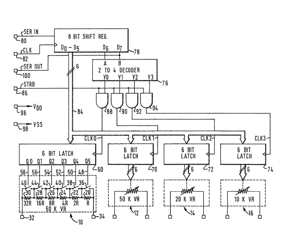
Turning now to the drawings, there is shown in
Figure 1 a functional block diagram of a single integrated
eireuit ineluding four variable resistor devices 10, 12, 14
and 16 accordin~ to the invention. Each variable resistor
device 10 to 16 is basically the same and therefore only
0 the device 10 will be described in detail.
The variable resistor device 10 is composed of
six resistances 20 to 30 wired in series between an input
eonnection 32 and an output connection 34. In parallel
across each resistance 20 to 30 is a respective elcctronic
analog switch 36 to 460 These switches are, for example,
in the form of field effect transistors having an
electrical conductivity varying from a low resistance in
the closed circuit condition to a high resistance in the
open circuit condition. They can be switched be-tween the
two conditions by a signal applied to their respective
gates or control inputs 48 to 5~.
One ~ind of well-known electronic switch suitable
for use in the present invention is a complementary
metal-o~ide-semiconductor (CMOS) bilateral switch. The
schematic diagram o~ such a switch 136 is shown in Figure 2
for the purpose of illustrating the advantages and
disadvantages o~ alternative constructions for the
electronic switches used in the present invention. The
CMOS bilateral switch 136 has a control input 138 and
switch terminals 140 and 142. The CMOS bilateral switch
136 also has connections to power supply voltages VDD and
Vss. The supply voltage VDD is positive with respect to
Vss .
In order to provide an open or closed circuit
between the switch terminals 140 and 142 in response to a
logic signal on the control input 138, the switch 136 has a
pair of insulated-gate field e~fect transistors 144 and 146
having their channels connected in parallel to the switch
terminals 140 and 142, and having their gates coupled to
the control input 13~. The transistor 144 has an n-type
channel rendereA conductive when thc voltage on its gate
becomes substantially positive with respect to th~ voltages
on the switch terminals 140 and 142. The transistor 146
has a p~t~pe channel rendered conductive when the voltage
- lO -
on its gate becomes substantially negative with respect to
the voltages on the switch terminals 140, 142. So that the
bilateral switch 136 is closed in response to a logic high
of about VDD on the control input 138 and open in response
to a logic low of about Vss, the gate of the transistor 144
is conneeted directly to the control input 138, and the
gate of the transistor 1~ is connected indirectly to the
eontrol input 138 via a CMOS inverter stage 148. The CMOS
inverter stage 148 includes an n-channel insulated-gate
field-efect transistor 150 and a p-channel insulated-gate
field-effeet transistor 152.
It should be apparent that n-ehannel field-effeet
transistors or p-channel field-effect transistors, or both,
ean be used as electronic switehes for the present
invention. By using both p-channe:1 and n-channel
transistors in eaeh elcctronic switch, the variable
resistors can handle any ~nalo~ signal within the range of
the power supply from Vss to VDD.
Returning now to Figur~ 1, it ean be seen that
the eleetronie switches 36 to 46 are controlled according
to data held in a 6-bit latch 60 having respective
single-bit outputs connected to the gate inputs ~8 to 58 o
the switches. Therefore, the latch 60 may receive a data
signal ~rom timc to timc and oncc a data signal has bccn
reeeived the single-bit outputs of the latch 60 will open
and close the switches as requi.red and maintain -that status
until a new data signal is received.
The values of each resistance 20 to 30 are in the
progression 2, 21, 22r etc, so that their absol~-te values
are R, 2R, 4R etc. In this way by appropriate opening and
closing of switches 36 to 46 the variable resistor can have
a value which varies step-wise in units of R from 0 to 63R.
For each variable resistor device 10 to 16 the absolute
value of R can be the same or different and is chosen
according to the circuit which it is to control. For
example~ the resistor devices 10 and 12 are shown in the
drawing as having a maximum resistance of 50 K ohms while
resistor 1~ has a maximum value of 20 K ohms and resistor
16 has a maximum value of 10 K ohms, all being variable in
increments of approximately l/64th of the maximum value.
In practice the electronic switches 36 to 46 have
a significant resistance when in their closed state.
Therefore, when all of the switchcs are closed, thc
variable resistor 10 will have a certain minim~n resistance
of r, where r is appro~imately the sum of the internal
resistances of the electronic switches. Preferably the
valùes o~ the individual resistances 20 to 30 and the
internal resistances of the switches are chosen so that the
resistance of the variable resistor can still be set
- step-wise in units of R to any value selected from the
series O+r, R+r, 2Rtr, 3R-tr and so on. This can bc done by
choosing the value of each individual resistor to include a
resistance of r/x in addition to -the basic chosen value of
the individual resistance R, where ~ is the total n~ er of
12 -
electronic switches, i.e. x is six for the variable
resistor 10. In other words, the first resistance should
have a value of R+r/x, the second resistance should have a
value of 2R~r/x, the third resistance should have a value
of 4R+r/x, and so on. Also, the internal resIstance of each
switch (in parallel combination with its respective
resistance) should provide a resistance of r/x when the
switch is in its closed state. Thus, irrespective of
; whether an individual electronic switch 36 to 46 is open or
closed there will be included between the input and output
connections 32 and 34, a constant additional resistance
value of rJx for each individual switch and resistance
pair.
The choice of resistance values according to the
above binary progression of R, 2R, 4R, e-tc. , provides a
direct correspondence between the numerical value
represented by the binary data signal held in the latch 60
and the resistance of the variable resistor 10. For
example, assuming that the single bit output Q0 represents
the "most significant bit" and the single bit output Q5
represents the "least significant bit", then if the data
were 2 representing a numerical value of 0, then all
switches would be closed resulting in a resistance value of
OR+rO If th~ data wcre 12 reprcsenting a nwllerical
value of 1, then the switch 38 associated with the
resistance 22 would be opened giving a value of lR-~r. If
the data were 001010~ representing a numerical value of 10,
- 13 -
then the switches 38 and 42 associated with the resistances
22 and 26 would be opened giving a value of lOR+r, and so
on.
In the example shown in the drawing the variable
resistor lO includes six resistances 20 to 30. There
could, be more or less. Thus if the latch 60 were to hold
an 8-bit "byte" then the variable resistor lO could have
eight resistances in series, if the data were a 4-bit
"nibble" then there could be ~our resistances, and so on.
As explained above the integrated circuit of
Figure l includes four resistor devices lO to 16 according
to the invention. The device lO has its own latch 60 while
the other resistor devices have their own respective
latches 70 to 74. It should be apparent that some means is
required for setting or resetting the latches with data in
such a way as to minimize the number of required
connections to the integrated circuit. For this purpose
the latches could be connected in a shift register
configuration so that data could be loaded into all of the
latches over a single serial input as a clocking signal is
applied to a clock input. Such a shift register
configuration, however, would re~uire all o~ the data in
all of the latches to be changed to change the data for any
one latch.
To supply data to a selected one of the latches,
the integrated circuit of Figure l includes a decoder 76
- ] ~ -
and a shi~t register 78. Data to be received in the
selected latch is transmitted to the shift register 78 from
a serial data terminal 80 as a clocking signal is applied
to a clock terminal 82. The data appear on parallel outputs
Do to D5 of the shift register and are transmitted over a
6 bit data hus 84 connecting respective data inputs of the
latches 60, 70, 72 and 74 in parallel. Only the selected
one of the ~our latches, however, receives the data from
the data bus 84, in response to a respective clock signal
(CLKO, CLKl, CLK2, C~K3).
To select a particular one of the four latches 60
to 74 for receiving -the six bits of data Do to D5, the
shift register has two additional outputs D6 and D7 which
together indicate or address the selected register. These
outputs are co~nected to a 2 to 4 decoder 76 providing four
outputs ~'0, Yl, Y2, Y3 so that only a selected one of the
outputs is active at any given time. The output signals
change, however, as data are shi~ted into the shift
register 78. To indicate when the shift register 78 has
received data for loading into a selected register, the
integrated circuit has a terminal 86 Eor receiving a strobe
signal (STRB). The strobe signal clocks the particular
latch being addressed by the outputs D6 and D7 at the time
that the strobe signal is applied. For this purpose the
respective clock signals CLK0, CLKl, Cl,K2, CLK3 are
obtained by gating the decoder outputs Y0, Yl, Y2, Y3 with
the strobe signal (STRB) as indicated by respective AND
- 15 -
gates 88, 90, 92 and 94. Alternatively, the decoder 76
could be constructed to receive the strobe signal to gate
0, Yl, Y2, Y3, as is done, for example in
conventional decoder integrated circuit part No. 74S139,
which is described on page 2:46 of the National
Semiconduetor TTL Da-ta Book, National Semiconductor
Corporation, 2900 Semiconductor Drive, Santa Clara, CA
95051 (1976).
As noted above, the integrated circuit of Figure
1 may be formed on a single normal sized integrated eireuit
ehip. In addition to the terminals diseussed above, the
integrated circuit chip has a power supply terminal 96 and
a ground terminal 98. These terminals are shown supplying
the voltages VDD, and Vss, which are fed to the logie
eomponents 60, 70, 72, 74, 76, 78, 88, 90, 92, 94 and the
eleetronie switehes 36 to 46. In this ease it is assumed
that these eomponents use CMOS logic elements although
alternatively the integrated circuit eould use n-MOS or
other kinds of logic elements.
~0 The integrated circuit of Figure 1 may fit in a
standard integrated circuit paekage such as a 14-pin dual
in-line package (DIP). As described above, 13 terminals are
: used for eonnections to the variable resistors, logie
eomponents, and power and ground for the integrated
eireuit. The 14th terminal 100 is conveniently used as an
output for serial data (SER OUT) from the shift register
78. Therefore two or more integrated eircuits similar to
- 16 -
the integrated circuit of Figure l are readily connected
together, with the serial data input 80 of a second chip
connected to the serial data output of a first chip, and
the respective clock 82 and strobe 86 terminals of the two
chips connected in parallel, to provide more than four
variable resistors for an exterl1al circuit.
Specific examples of resistances which can be
produced with particular input values of an 8 bit byte of
data Do to D7 are shown below in the following Table I.
:` 10
~0
TABLE I.
DATA INPUT RESISTANCE 6 7 = 10 = 01 = 11
O 1 2 3 4 5 RES 10 RES 12 RES 14 RES 16
0 0 0 O 0 0 OR 3 KQ 3 ~Q 3 KQ 3 8Q
. _ _ _
0 0 0 0 0 1 R 47/63 47/63 17/63 7/63
-t3 _3 +3 _ ~3
=3.75 KQ =3.75 8n =3.27 8Q =3.11 8Q
O 0 O O 1 O 2R 2(47/63) 2(47J63) 2(17/63) 2(7/63)
+3 _ +3 -13 +3
=4.50 KQ =4.50 Kn =3.54 Kn -3.22 KQ
. _ _ _ . _ _ _ . _ . . . _
1 1 1 1 1 1 63R SO RQ 50 KQ 20 KQ 10 KQ
. . _ . _ . . . _ _ _ . .
' ' . :
':
- 18 -
Turning now to Figure 3, there is shown a
timing diagram for the case where the data are 01001101 10.
Irrelevant portions of the signals are shown as a string of
periods ( ... ). The data are supplled to the serial input
terrninal 80 in Figurc 1 and loaded in-to the shift register
78 b~ applyin~ the clock signal (CLK) to the clock terminal
82. After eight clock cycles, the data is properly
aligned in the shift register for loading into the selected
latch 70. At this time the address for the selected latch
appears on the outputs D6 and D7 of the shift register, and
the strobe is applied on the strobe terminal 86 to clock
the selected latch 70. Only the decoder output Y1 is a
logic high when the strobe is applied. Therefore, only the
CLKO signal is active and the data Do to D5 is received
only in the selected latch 70.
In view of the above, there has been described
a compact and inexpensive variable resistor whose value of
resistance can be set by a data signal. To reduce the size
of the variable resistor, the variable resistor includes a
number of variable resistances connected in series, and an
individual electronic switch connected in parallel across
each individual resistance. Preferably the values of the
individual resistances are chosen from the progression
2,21~22,23, and so on, so that the resistance of the
variable resistor corresponds to the binar~ value of data
applied to control the elec-tronic switches. At least four
such variable resistances can be constructed on a single
normal size integrated circuit chip. The integrated
circuit includes a latch to hold the data signal until a
new data signal is receivedO To minimize the number of
connections to the chip, the integrated circuit further
includes a shift register and a decoder to supply a
selected latch with data from a serial data stream.
' 10
,