Note: Descriptions are shown in the official language in which they were submitted.
200667;~
Description
CAPACITIVE PRESSURE SENSOR WITH THIRD ENCI~CLING PLATE
Technical Field
This invention relates to pressure sensors utilizing
capacitance variations to sense pressure variations, and more
particularly the present invention re~ates to silicon-gla~s-
silicon pressure sensor designs which employ a silicon dia-
phragm, the movement of which due to changes in pressure varies
the capacitance of the sensor and thus provides an output
representative of the applied pressure. Even more particu-
larly, the present invention relates to the minimizing of the
long term drift and the parasitic (non-pressure sensitive)
capacitance which occur in such sensors.
Back~round Art
Capacitive pressure sensor~ are well known and are
employed in capacitance transducers, microphones, rupture
discs, resonators, vibrators and like devices. Many of the
- applications for such capacitive pressure sensors require that
the sensors be extremely small, for example, of the order of
eight millimeters by eight millimeters (8 mm x 8 mm).
Silicon capacitive pressure transducer~ are known in the
art. For example, U.S. Patent No. 3,634,727 to Polye discloses
one type in which a pair of centrally apertured, conductive
.~
200667~
--2--
~ilicon plates are joined together with a eutectic metal bond,
suc~. th~t t~e ~ilicon diss plates fle~ with ~pplied pressuret
changing the cap~citance of the aperture interstice and
providing a capacitive-type signal manifestation of pressure
magnitude. This form of pressure transducer thus relies on the
pres~ure-induced deflection of a thin diaphragm, in which the
diaphragm deflection as a ~unction of fluid pressure causes a
variation in the distance between a pair of surfaces which
effectively form the plates of a variable capacitor. Other
examples of such silicon pre~sure sensors or transducers are
included in the U.S. patents listed below.
However, long term drift and parasitic (non-pressure
sensitive) capacitance are problems which detract from the high
sensitivity and accuracy required for, for example, demanding
aerospace applications of such capacitive pressure sensing
devices.
In present state of the art silicon-glass-silicon (SGS)
capacitive sensors, the glass annulus 16 around the sensor
(note Figures lA & 1) constitutes a necessary part of the
structure but is the source of a pressure-insensitive capaci-
tance, which adds in parallel to the pressure-sensitive
capacitance of the sensor. This reduces the dynamic range of
the sensor and reduces its sensitivity to pressure changes.
Also, because of the inherently long term instability of
the glass dielectric constant, this parasitic glass dielectric
capacitor can result in an overall long term drift, which must
be reduced or compensated for in order to realize aerospace
performance.
Other approaches have taught the fabrication of a three
terminal (or three plate device) which, when combined with
appropriate circuitry, eliminates the parasitic capacitance
- from the measurement and, thus, eliminates the drift and
instability. The sensors described in assignee's U.S. Patent
No. 4,467,394 of Grantham & Swindal (see Figure 2 hèreof) use a
metal plate 120 inside the reference cavity 114 with a feed-
- Z0(~667~
.
--3--
through sealed inside the glass sealing ring 116 for the third
plat~ 120. ~Iowever, in this approach, a non-planar structure
resultR, which poses special sealing problem~. In addition,
definition of the metals chosen presented special problems in
5 defining the shape by chemical etching.
Some exemplary, prior art, U . S . patents in the f ield of
capacitive pressure sensors or transducers, owned by the
assignee hereof, are listed below:
Patent N~. Title Inventors Issue Date
10 4,530,029 Capacitive Pressure C . D . Beri~tain 07/16/85
Sensor With Low Para-
sitic Capacitance
4,517,622 Capacitive Pressure B. Male 05/14/85
Tr~n~ r Signal
Conditioning Circuit
4,513,348 Low Parasitic D.H. Grantham 04/23/85
Capacitance Pressure
Tr~n~ r and Etch
Stop Method
20 4,467,394 Three Plate Silicon- D.H. Grantham 08/21/84
Glass-Silicon J.L. Swindal
Capacitive Pressure
Tr~n~r
4,463,336 Ultra-Thin Microelec- J.F. BIack 07/31/84
tronic Pressure T.W. Grudkowski
Sensors A. J . DeMaria
4,415,948 Ele.;l.~3tatic p~nrl~ D.H. Grantham 11/15/83
~ilicrn Capacitive J . L. Swin~ 1
Pressure l~nR~I~c~r
30 4,405,970 Silicon-Glass-Silicon J .L. Swi~ldal 09/20/83
Capacitive Pressure D.H. Grantham
Tr~n~l~c~r
Di~clo~ure o~ Invention
The present invention is directed to over-come or at
35 least minimize the problem of the additive pressure-
insensitive capacitance of the non-conductive glass
2006672
-
annulus, without introducing any of the additional
problems of the other approaches to this problem in
the prior art.
The present invention achieves this goal
by including a thin, third capacitive plate, not
within the central region of the sensor, but rather
outside of the central region encircling it.
Aspects of the present invention include
the choice of materials, preferably with all three
plates being of conductive, doped silicon or at
least preferably of the same material, a symmetrical
placement of the third silicon plate encircling the
central region rather than being positioned within
it, and improved assembly techniques for higher
manufacturing yield and better long term
reliability, with preferably all layers being
planar.
In accordance with a particular embodiment
of the invention there is provided a capacitive
pressure sensor of the conductor-dielectric-
conductive type, comprising:
a conductive substrate forming a first
capacitive plate;
a conductive flexible, elastic diaphragm
having an exterior side, said diaphragm being
capable of flexing movement due to changes in
pressure on its exterior side and forming a second
capacitive plate; and
a non-conductive, dielectric layer between
said conductive substrate and said conductive
diaphragm, said layer providing peripheral wall
spacer(s) extending between and joining said
conductive substrate and said conductive diaphragm;
an evacuated chamber being formed between said
substrate and said diaphragm and being closed off by
spacer wall(s) formed by said dielectric layer
_
- 4a -
- ` 2006672
between said substrate and said diaphragm; the
flexing movement of said diaphragm due to the
changes in pressure on its exterior side causing the
capacitance of the sensor to vary; said c-hamber
being at least generally cylindrical in its outer
configuration defining a central region; and
a third, conductive plate located in said
wall(s) spaced and separated from both said
conductive substrate and said conductive diaphragm
by said dielectric layer and forming a third
capacitive plate, said third conductive plate
encircling said central region but being located
substantially outside of said central region.
From a different aspect, and in accordance
with a particular embodiment of the invention there
is provided a method of minimizing the parasitic
capacitance of a capacitive pressure sensor, which
sensor includes -
- a conductive substrate;
- a conductive diaphragm having an
exterior side, said diaphragm being capable of
flexing movement due to changes in pressure on its
exterior side; and
- a non-conductive, dielectric layer
between said conductive substrate and said
conductive diaphragm, said layer providing
peripheral spacer wall(s) extending between and
joining said substrate and said diaphragmi an
evacuated chamber being formed between said
substrate and said diaphragm and being closed off by
said peripheral spacer walls(s) formed by said
dielectric layer between said substrate and said
diaphragm; the flexing movement of said diaphragm
due to the changes in pressure on its exterior side
causing the capacitance of the sensor to vary;
comprising the following step(s):
~,
~ .
- 4b -
2006672
providing a third, conductive plate in
said spacer wall(s) spaced and separated from both
said conductive substrate and said conductive
diaphragm by said dielectric layer, with said third
conductive plate encircling said central region but
being located substantially outside of said central
region.
The foregoing and other features and
advantages of the present invention will become more
apparent from the following further description and
drawings, in which like reference numbers are used
across the figures to denote common or analogous
elements or structures.
Figure lA is a perspective, partially cut-
away view of a silicon-on-silicon, two plate
capacitive pressure sensor of the prior art, which
has. some common structural and operational
characteristics as the sensor of the present
invention; while
Figure 1 is a side, simplified view of a
silicon-on-silicon, two plate capacitive pressure
sensor of Figure lA, but with the pressure port
transition piece removed to better show the parts
more relevant to the present invention.
Figure 2 is a side, simplified view of a
silicon-on-silicon, three plate capacitive pressure
sensor of the
- 2006672
prior srt, with the added third plate being contained
centrally with~n the central region of the sensor.
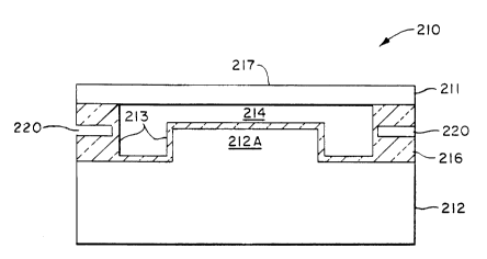
Figure 3 is a side, .~implified view of an exemp.lary
embodiment of a silicon-glass-silicon (SGS) capacitive
pressure sensor of the present invention, the sensor being
basically cylindrical in shape and symmetrical about its
vertical, longitudinal center line in its central region
and being square or cylindrical in its outer configura-
tion, with its third plate being positioned outside of the
central region of the sensor within the glass spacer wall,
encircling the central region.
Figure 4 is an electrical schematic diagram of the
equivalent electrical circuit of the sensor of Figure 3.
Best Mode for CarrYin~ Out the Invention
- Two Plate Sensor (Prior Art - Figs. 1 h lA) -
For a better understanding of the general structure
and operational characteristics of the two plate portion of
the present invention, a simplified two plate sensor of the
prior art will be discussed with reference to Figures lA &
1 for general background information.
In the exemplary prior art, silicon-glass-silicon
single pressure sensor design of the sandwich type of
Figures lA & 1, a dielectric wall spacer 16 is located
between a silicon diaphragm 11 and a silicon base 12. The
dielectric wall spacer is typically made of borosilicate
glass.
The dielectric layer 13 between the diaphragm and
base, particularly in the upwardly extending wall support
or spacer area 16 formed by the dielectric layer at the
operative periphery of the sensor, comprises approximately
- fifty (50X) percent of the total capacitance of the sensing
element. In the present invention this parasitic capaci-
tance, located typically at the periphery of the device,
-6- 2006672
generally identified as "Cv", is minimized if not
eliminated
As can be seen in Figure lA, the exemplary prior art
silicon-on-silicon pressure sensor or transducer 10 typic-
ally is generally s~uare in its exterior configuration butoften at least generally and preferably is circular or
cylindrical in shape for its inner, operative ~ubstructure,
which constitutes its central region Cc.
The sensor 10 includes an upper, conductive, square,
flexible, appropriately doped, silicon diaphragm 11 and a
lower or bottom, conductive, appropriately doped, silicon
base or sub~trate 12 with a non-conductive dielectric layer
and spac-er 13 (made of, for example, borosilicate glass)
between them, a closed, evacuated, hermetically sealed,
reference cavity, chamber or interstice 14 being formed
between the two silicon layers 11, 12. The chamber 14 is
typically at a zero vacuum or can be sealed at a higher
reference pressure, at which reference level the diaphragm
11 is parallel to the silicon substrate 12, with typically
a two micrometer spacing between the two.
It should be understood that the simplified drawings
hereof for practical purposes of illustration are not at
all to relative scale, as the glass wall or spacer 13/16 is
only typically nine micrometers high, in contrast to the
2~ thicknesses of the silicon layers 11 & 12, which typically
are eight thousandths (0.008") of an inch and fifty
thou~andths (0.050") inche~ thick, respectively, for an
exemplary fifty (50 psi) pounds per square inch pressure
measuring unit.
A centrally located, typically circular pedestal or
mesa 12A extends into the typically generally cylindrical,
closed chamber 14 with a thin, insulating layer of glass
13A (not shown in Fig. lA) covering the top of the mesa.
Due to the thinness of the layer 13A, typically only a half
of a micrometer, which is usually deposited after the
ZOO~i67Z
relatively high wall 16 (typically nine micrometers), it
typically play5 no significant role in the paraqitiç
capacitance of t~e sen~or 1~.
As the external ambient pressure on the outside of the
~ensor 10 varies, the diaphragm 11 flexes downwardly,
causing the spacing between the silicon layers 11 ~ 12,
serving as capacitive plates, to change and lessen, in turn
changing the capacitance of the sensor. This change in
capacitance as a result of a change in the exterior
pressure on the exterior surface or upper-side 17 of the
diaphragm 11 is used as a measure of the pressure and its
changes.
Conductors or electrode~ 18A & 18B to the silicon
layers 11 & 12 are included for connecting the transducer
or sensor 10 into an appropriate circuit, many of which are
known to the art, which measures its changing capacitance
a~ a function of the pre~sure. The varying pressure on the
exterior, sensing surface 17 of the ela~tic silicon
diaphragm 11, causing the diaphragm to flex and relatively
unflex, changes the value of the interstitial capacitance
between the diaphragm and the electrode to the lower
silicon substrate 12, which transduces the applied pressure
to a measurable electronic signal. Typically, as noted
above, there is about an exemplary two micrometer gap
between the inner, lower, underside surface of the
diaphragm 11 and the top or upper-side of the mesa 12A,
when the sensor is at its zero or-reference pressure, to
allow room for the diaphragm to flex inwardly toward the
mesa 12A, as the pressure increases.
The wall(s) 16 might typically have a horizontal,
lateral or radial thickness of, for example, thirty-six
thousandths (0.036") of an inch with a height of, for
example, nine (9) micrometers, while the separately
applied, insulating, mesa layer of glass is only about a
half a micrometer thick. The mesa 12A extends up from the
` 2006672
--8--
main surface o~ the ~ilicon substrate 12 an exemplary six
and a half micromet~rs, ~hile ~aving an exe~larY dia~eter
of one hundred and fifty thousandths (0.1~0") of an inch~
The silicon diaphragm 11 and the silicon base 12 may
typically be square [with corners removed for the purpose
of providing access for electrical contacts to the lay-
er(s), as illustrated], having a horizontal length of an
exemplary two hundred and sixty thousandths (0.260") of an
inch on an edge, while the spacer wall 16 can have an inner
diameter of an exemplary one hundred and ninety thousandths
(0.190") of an inch. The outer, side surface of the wall
spacer 16 can either follow the basic square configuration
of the silicon layers 11/12 or have an outer circular
configuration.
A transition piece 18 is bonded through an exemplary
glass layer 20 to the upper, exterior surface 17 of the
diaphragm 11 and includes a pressure port 19, through which
the pressure to be sensed i~ communicated to the diaphragm.
In turn the sensor 10 is appropriately mounted for use in
the desired application.
- Three Plate Sensor (Prior Art - Fig. 2) -
The prior art, three plate sensor illustrated in
Figure 2 is similar to the two plate ~ensor of Figures lA &
1, with the exception that a third conductive plate 120
has been added within the very central region of the sensor
110. This third plate is typically made of metal, rather
than doped silicon, and extends out in a sealed
feed-through 121 through the side wall 116A from the
chamber 114, in order to have electrical contact made to
it.
As can be clearly seen in Figure 2, this result~ in a
non-planar arrangement, particularly for the glass layers
116/116A.
The silicon diaphragm 111 and the base 112 operate in
similar fashion to the diaphragm 11 and the base 12 of the
-
Z00667Z
-
g
sensor 10. For further information on this type of three
plate, pr~or art ~en~or, reference i~ had to the '3~4
patent of Grantham & Swindal referred to above.
Such prior art, three plate sensors have the long term
drift and parasitic capacitance problem~ the present
invention is designed to overcome or at least minimize,
without having to use circuitry added for this purpose.
- Three Plate Sensor of Invention (Fig~. 3 ~ 4) -
In contrast to the prior art sensors oi Figures 1 & 2,
the three plate sensor 210 of the present invention, asexplained more fully below in connection with Figures 3 &
4, includes a third plate 220 preferably made of doped,
conductive silicon, which is located within the glass
spacer wall 216 and encircles or extends around the central
region of the sensor 210, rather than being located within
it. The third capacitor plate 220 is symmetrical about the
vertical, longitudinal center axis of the sensor 210 and is
basically in the shape of a flat washer and forms an
annulus, if the sensor has a cylindrical outer configura-
tion. With this approach, no feed-through through the
spacer wall 216 into the chamber 214 is necessary to make
electrical connection to the third plate 220, as the outer
edge of the third plate 220 is readily available and
accessible for making an electrical connection to it.
Figures 3 and 4 are generalized or schematic represen-
tations of a capacitive pressure sensing device, in
accordance with the principles of the present invention,
with the third plate 220 preferably being made of a very
thin layer of electrically conducting polycrystalline
silicon or, if so desired, a metal or other conductive
material. The three plates 211, 212 & 220 are preferably
~ made of the same materials, with that material preferably
being electrically conducting, polycrystalline silicon.
Conductors or electrodes (not illustrated for simplic-
35 ity purposes in Figure 3 but similar to those 18A & 18B of
- - 2006672
--10--
Figure lA) to the conductive silicon diaphragms 211 and to
~hc ~c~duct~-~e ~i 1 icon ba~es 212, as well a~ to ~he t~r~
silicon plate 220, are included for connecti~ the
transducer or sensor 210 into an appropriate circuit, a
number of which are ~nown in the art. The circuit measures
the changing cap~citances a5 an inverse function of the
pre~sure on the outer side 217 of the diaphragm 211
communicated through it~ pressure port (not illustrated),
causing the diaphragm to flex, changing the value of the
capacitance, which transduces the applied pressure to
measurable electronic signals.
Some of the advantages which this structure of the
invention has over other three plate configurations, such
as the prior art one shown in Figure 2, is in its cylindri-
cal symmetry, the preferred choice of silicon as a materialfor compatible propertie~, and the planarity of the ~ealing
surfaces, with consequently seals of high integrity.
The fabrication could be effected in a manner similar
to that already described in other patent~ - namely
assignee's U.S. Patent No. 4,415,948 of Grantham & Swindal,
listed above, for example.
A glass layer 213 is first deposited on the shaped
silicon base 212 by sputtering, ion beam sputtering, or
other suitable technique. Then, in accordance with the
invention, a very thin, polycrystalline (or amorphorous)
silicon layer is next deposited to a thickness of, for
example, about one micrometer, although other dimensions
may be used, if other considerations dictate it, without
altering the desired performance.
Next a further layer of glas~ 213 is deposited. Then
a corner of the third plate is exposed by etching, sawing
or other means. This exposed corner can be used for
electrostatic bonding of the silicon diaphragm 211 to the
base structure.
-
` - ~
2006672
The necess~ry photolithography and etching steps for
de~i~ition o~ the re~erence cavity 214, that is, the
e~closed, evacuated chamber, and the delineation of the
silicon third plate 220 are well known to those of ordinary
skill and, for brevity ~ake, are not described here.
When the materials of construction are conductors
other than silicon and the spacer-insulator is a material
other than glasx, similar considerations to the foregoing
apply, and a third plate analogou~ly can be incorporated in
the structure as described above for silicon.
With reference to the schematic of Figure 4, in the
sensing circuit used, which is basically a Schmitt trigger,
the potential of the ba~e 212C is maintained at the third
intervening plate potential 220C by the op-amp 230. If the
mid-point of the series connected capacitors is maintained
at the same potential as the voltage input, no charge flows
through branch "B" from the source at the diaphragm connec-
tion 211C. Thus, the parasitic and unstable glass
dielectric properties are eliminated from the measurement.
Exemplary dimensions for the three plate pressure
sensor 210, not previously detailed with respect to the
exemplary two plate pressure sensor 10 above or otherwise
provided above, are outlined below.
The third plate 220 could have an exemplary thickness
of a micrometer, with there being an exemplary half of a
micrometer thickness of glass between the inner diameter of
the third plate and the outer diameter of the chamber 214.
The outer diameter or width of the third plate 220 could be
an exemplary two hundred and sixty thousandths (0.260") of
an inch, with an inner, exemplary diameter of one hundred
and ninety thousandths (0.190") of an inch minus a
micrometer. The thickness of the glass layers 213 above
and below the third plate 220 could be an exemplary six
micrometers.
.
- Z00667Z
-12-
It should be understood that in using the terms
"above" or "below". "down" or "up", or "vertically" or
"horizontally," these terms are being used in an exemplary
relative sense, as presented in the drawing~ hereof. Thus,
for example, in a particular application the silicon
substrate could in fact, of course, be below the diaphragm
and, rather than the Qilicon layers being horizontally
diqpoQed with the wall spacer being vertical, the silicon
layers could be vertically disposed or disposed at an acute
angle to the horizontal, with the dielectric layer
appropriately positioned relative to them.
Although this invention has been shown and described
with respect to a detailed, exemplary embodiment thereof,
it -~hould be understood by those skilled in the art that
various changes in form, detail, methodology and~or
approach may be made without departing from the spirit and
scope of this invention.
Having thus described at least one exemplary embodi-
ment of the invention, that which is new and desired to be
secured by Letters Patent is claimed below.