Note: Descriptions are shown in the official language in which they were submitted.
OD OF NAN~FACTURINa M~LTILAY~RFD pRIN~D-~IRING-BoaRD
BACKGROUND OF THE INVENTION
: 5 Field of the Invention
:~,
This invention relates to the production of
multilayered printed-wiring-boards, and more particularly
to a method of manufacturing a multilayered printed-
wiring-board by electrically connecting a plurality of
printed-wiring-boards (hereinafter called "PWBH)
~; together.
., .
' i:
~RIE~ ~E~BIpIIoN-o-F-T~El~R~wlNGs
FIG. 1 is a cross-sectional view of components
for manufacturing a multilayered PWB in a method
according to a first embodiment of this invention;
~, FIG. 2 is a cross-sectional view of the
components of FIG. l, showing them after having been
processed by pressurizing and heating;
~ .,
~ FIG. 3 i~ a cross-~ectional view of components
" .
for manufacturing a multilayered PWB in a method
according to a second embodiment;
FIG. 4 is a cross-sectional view of the
components of FIG. 3, showing them after having been
processed by pressurizing and heating;
.,,,~,x~
,,
..
~ A
,.
`.. ;,. . .. ` . ` ` ` .
~r..
~,:' ' ; : ` ' `
:.', t ` : :,~ : . .:
~'':,: ` : ' '
~: :
FIG. 5 is a cross-sectional view of components
for manufacturing a multilayered PWB in a method
according to a third embodiment;
FIG. 6 is a cross-sectional view of the
components of FIG. 5, showing them after having been
processed by pressurizing and heating;
FIG. 7 is a cross-sectional view of components
for manufacturing a multilayered PWB in a method
aceording to a fourth embodiment;
FIG. 8 is a cross-sectional view of the
components of FIG. 7, showing them after having been
processed by pressurizing and heating;
FIG. 9 is a cross-seetional view of components
for manufacturing a multilayered PWB in a method
lS according to a fifth embodiment;
FIG. 10 is an enlarged cross-seetional view
showing the junction between a solder bump and a
conductive layer in the fifth embodiment;
FIG. llA is a cross-seetional view of
components for manufacturing a multilayered PWB in a
~ method according to a sixth embodiment;
;`' FIG. llB is an enlarged cross-seetional view
showing the surfaee of a conductive layer in the sixth
~;~. embodiment;
FIG. 12 is a cross-sectional view of components
for manufaeturing a multilayered PCB by adapting the
: .~
~ method of the sixth embodiment;
. j
- 2 -
;
A.' '~
:~ .
",:. . ~
.. .
FIG. 13 is a cross-sectional view of components
for manufacturing a multilayered PWB in a prior art
; method;
FIG. 14 iB a cro8s-sectional view of the
components of FIG. 13, showing them after having been
processed by pressurizing and heating and also by forming
through-hole8; and
FIG. 15 iS a cro88-8ectional view of the
component8 of FIG. 14, 8howing them after the through-
holes have been plated.
:.
~çscription Of the Related Art
Heretofore, attempt8 have been made to install
circuit elements on a 8ub8trate With high-concentration
to realize an integrated circuit board. To thiS end, it
; is a known practice to u8e a multilayered PWB, in which
` insulating and conductive layer8 are placed alternately
^one over another. Another popular method is to use a
multilayered printed-circuit-board ~hereinafter called
~multilayered PCBn), in which variou8 circuit elements
~are in8talled on and/or inside a multilayered PWB.
.l The multilayered PWB and PCB are particularly
` useful when realizing a compact-8ized and high-
~' 25 concentration circuit of high freguency, 8uch as 400 MHZ
band, 800 - 900 MHz band and 1.5 GHz band, in automobile
and portable telephone8, for example.
.
.. - 3 -
... .
.. , ' .
`~
In the manufacture of a multilayered PWB or
PCB, it is known to unify a plurality of PWBs by
superimposing.
As is well known in the art, a PWB is produced
by providing a conductive layer on the surface of an
insulating substrate and forming an additional conductive
layer thereover in a desired pattern according to need.
` A copper foil or a conductive paste, for example, is used
~ for the conductive layer.
- 10 Further, a PWB having a conductive layer on
only one of opposite surfaces is called a single-face
PWB, while a PWB having a conductive layer on either one
of opposite surfaces is called a double-face PWB.
FIGS. 13 through ~5 are cross-sectional views
showing progressive manufacturing steps of a multilayered
PWB according to the typical conventional method, which
` will now be described in greater detail. The
conventional production of a multilayered PCB is similar
-~j to that of a multilayered PWB except for an additional
i}
~' 20 step of installing circuit elements, and therefore, its
-j detailed description is omitted here for clarity.
`4, In FIG. 13, two single-face PWB 10, 12, a
double-face PWB 14, and two inter-layer adhe6ive sheets
;~ .
;j 16, 18 are shown.
~ 25 Each of the single-face PWB 10, 12 is composed
, ~-
of an insulating substrate 20, 22, and a conductive layer
' 24, 25 in the form of a copper foil attached on one
:-i
- 4 -
....
~ . ,,
'' -' '
surface of the insulating substrate 20, 22. The
conductive layer 24, 25 is free of patterning.
The double-face PWB 14 is composed of an
insulating substrate 26, and conductive layers 28 and 30
attached on either one of opposite surface of the
insulating substrate 26. The conductive layers 28 and 30
are previously formed in a pattern necessary to realize a
desired circuit.
The conductive layer 24, 25 has a thickness of
about 18 to 35 ~m, for example, while the conductive
layer 28, 30 has a thickness of about 70 ~m, for example.
Thus the conductive layer 28, 30 is larger in thicknes3
than the conductive layer 24, 25 for securing reliability
of connection between the conductive layers 28, 30 and
; 15 the through-holes after the through-hole forming
; described below.
The inter-layer adhesive sheet 16, 18 i8 a
sheet commonly called ~prepregn. The inter-layer
adhesive sheet 16, 18 is formed of an epoxy resin
material curable under a predetermined curing condition
~ i
(i.e., temperature and time). In general, this material
~i~ is very popular for inter-layer adhesive sheets.
`~ In production, first of all, these components
i:
~i~ are placed one over another.
:-,
` ~ 25 For example, as shown in FIG. 13, the single-
~ face PWB 10, the inter-layer adhesive sheet 16, the
.''3 double-face PWB 14, the inter-layer adhesive sheet 18,
~;~
.~
~ - 5 -
F A~
,
-,-,- , :: - . , . ,- : : .- -^
: .
, ~ ;~ i .
and the single-face PWB 12 are placed one over another in
this order.
Further, the conductive layer 24 of the single-
face PWB lo faces upwardly, while the conductive layer 25
of the other single-face PWB 12 faces downwardly.
Namely, these two single-face PWBs 10, 12 are placed in
such a manner that their respective conductive layers 24,
25 face outwardly in opposite directions.
In this superimposed position, all of the
superimposed components are heated at a predetermined
temperature for a predetermined time, with applying a
pressure in the direction of superimposing. At that time
the adjacent superimposed parts come into contact with
each other.
For example, all of the superimposed components
are clamped between a pair of flat stainless plates in
the direction of superimposing, and are pressed by a
pre6sure of 30 kgf/cm2. At that time, they are heated at
a temperature higher than a curing temperature of the
~,
inter-layer adhesive sheet 16, 18, e.g., 170C, for 90
minutes.
-j Under this pre~sure and heat, the inter-layer
~- adhesive sheets 16, 18 are cured to form a pair of
;s insulating layers 32, 34 covering the conductive layers
~-~ 25 28, 30 of the double-face PWB 14. In addition, the
single-face PWBs 10, 12 are adhered one to each surface
~ of the double-face PWB 14 by the respective insulating
;~ layers 32, 34.
~ .
-- 6 --
S . , . ?
.. ~
Then, sub-through-holes 36 are formed through
the superimposed components at predetermined positions in
the direction of superimposing, as shown in FIG. 14.
As the inner surface of the individual sub-
through-hole 36 is plated to extract copper, the
conductive layers 24, 28, 30, 25 are electrically
connected at portions where the sub-through-holes 36 are
formed, as shown in FIG. 15. This is, the conductive
layers 24, 28, 30, 25 are electrically connected by
through-holes 38 having an inner surface coated with
copper.
Subsequently, the conductive layers 24, 25 are
processed by patterning. If the patterning was done
before forming the sub-through-holes 36, an accurate
.
~ 15 pattern could not have been achieved. This is the reason
, .~
why the patterning is done after having formed the
.
through-holes. As a result, a multilayered PWB has been
completed in which a desired circuit is formed as
=~; patterns of the conductive layers 24, 28, 30, 25. In
;'t 20 this conventional case, there are four conductive layers,
, ,.
~ which thus constitute a four-layered PWB.
. .
i; In the conventional art, a plurality of PWBs
are superimposed into a unitary form, and then the
conductive layers of the PWBs are electrically connected
. ~., .
by through-holes.
.,
However, if the sub-through-holes are formed
after the PWBs have been superimposed into a unitary
~'t form, good smearing is difficult to achieve.
- 7 -
. .,.~.~
-
.
.
Further, in the conventional manufacturing
method, after having formed the sub-through-holes, it is
necessary to take a wet processing such as plating and
patterning.
But if a liquid penetrates into the
multilayered PWB during the wet processing, it would
result in various troubles such as oxidation of the
conductive layers, and short-circuit between the
patterns.
With the conventional methods, only a limited
rate of production of good quality multi-layered PWBs can
,
be achieved. The same can be said of multilayered PCBs.
SUMMARY OF THE INVENTION
5i
`~i 15 It is therefore an ob~ect of this invention to
- provide a method of manufacturing multilayered PWBs at a
."
high rate of production of good quality products, without
forming any through-hole as a means for electrically
connecting conductive layers on PWBs.
According to a first aspect of this invention,
.~7~ there i8 provided a method of manufacturing a
,..,~
multilayered printed-wiring-board, comprising the steps
of (a) attaching a conductive member on a partial surface
of a conductive layer formed on at least one of opposite
surfaces of a printed-wiring-board in a pattern; (b)
superimposing a plurality of said printed-wiring-boards
one over another in 6uch a manner that said conductive
member formed and attached on said conductive layer on
- 8 -
... .
. .
one of said printed-wiring-boards confronts either said
conductive layer or said conductive member on another
printed-wiring-boards, at least one of said plurality of
printed-wiring-boards having been processed by said
attaching step; and (c) after said superimposing step,
electrically connecting said conductive member to either
said confronting conductive layer or said confronting
conductive member to form an electrical connecting layer,
characterized by applying over the surface of said
` lO conductive layer a buffer layer before said attaching
step for buffering a thermal stress resulting from a
-~ difference in coefficient of thermal expansion between
said conductive layer and said conductive member.
According to a second aspect of this invention,
. 15 th~re is provided a method of manufacturing a
~;i multilayered printed-wiring-board, comprising the steps
of: (a) attaching a conductive member on a partial
- surface of a conductive layer formed on at least one of
.~ opposite surfaces of a printed-wiring-board in a pattern;
,
`-I 20 (b) attaching an electrically insulating member on a
. partial surface of said conductive layer at at least a
conductive-member-free portion thereof; (c) superimposing
a plurality of printed-wiring-boards one over another in
such a manner that said conductive member attached on
said conductive layer on one of said printed-wiring-
boards confronts either said conductive layer or said
~`~ conductive member on another printed-wiring-boards, at
least one of said plurality of printed-wiring-boards
_ g _
.:
having been processed by the first-named attaching step
and the second-named attaching step; and (d) after said
superimposing step, electrically connecting said
conductive member to either said confronting conductive
layer or said confronting conductive member to form an
electrical connecting layer characterized by that said
electrically insulating member includes an insulating
adhesive resin, curing said insulating adhesive resin at
a predetermined temperature forming a unitary insulating
between the conductive layers.
; According to a third aspect of this invention,
there is provided a method of manufacturing a
multilayered printed-wiring-board, comprising the steps
of: (a) attaching a conductive member on a partial
~ 15 surface of a conductive layer formed on at least one of
: opposite surfaces of a printed-wiring-board in a pattern;
(b) disposing at least one distance element between the
~ printed-wiring-boards to be superimposed; (c)
superimposing a plurality of printed-wiring-boards one
over another in such a manner that said conductive member
formed and attached on said conductive layer on one of
said printed-wiring-boards confronts either said
conductive layer or said conductive member on another
printed-wiring-boards, at least one of said plurality of
printed-wiring-boards having been processed by said
attaching step; (d) after said superimposing step,
electrically connecting said conductive member to either
said confronting conductive layer or said confronting
-- 1 0 --
, ~
conductive member to form an electrical connecting layer,
characterized by that said distant element i5 a plurality
of spacer pieces each having a substantially constant
thickness, that said conductive member is a solder
material on a conductive resin, and mixing said spacer
:~ pieces in said conductive member keeping the distance
between the conductive layers constant; (e) superimposing
a plurality of printed-wiring-boards one over another in
~ such a manner that said conductive member formed and
::~ 10 attached on said conductive layer on one of said printed-
' -:
wiring-boards confronts either said conductive layer or
said conductive member on another printed-wiring-boards,
~; at least one of said plurality of printed-wiring-boards
`~ having been processed by said attaching step; and (f)
~; 15 after said superimposing step, electrically connecting
said conductive member to either said confronting
conductive layer or said confronting conductive member to
form an electrical connectihg layer.
.~ In the first method of this invention, an
electrical connecting layer connects the conductive
layers of a plurality of PWBs by the conductive member
attached on a partial surface of the conductive layer of
the individual PWB. It is therefore possible to avoid
~-i defects, such as inadequate smear, inadequate
penetration, etc., resulting from the forming of through-
holes. Also, it is needless to make the thickness of the
individual inner conductive layer larger than that of the
individual outer conductive layer. Further, the
,.
-- 11 --
A
outwardly facing conductive layer of the outmost PWB may
be previously processed by patterning.
The same results as the first method can be
obtained with the second method. An additional re~ult
with the second method is that $nsulat$on between the
conductive layers can be achieved at desired positions.
The same results as the first method can be
obtained with the third method. In addition, it is
possible to attach the conductive member within a desired
section with improved precision, thus causing an improved
; pattern accuracy and a high concentration of pattern.
; The PWB may be either a single-face PWB or a
; double-face PWB.
; If a buffer layer is attached over the surface
. .
of the conductive layer, a thermal stress acting on the
conductive layer i8 reduced.
; Also it is possible to install circuit elements
on the conductive layer.
Further, the conductive member may be either a
solder material, e.g., a solder paste having a
predetermined melting point or a conductive resin having
a predetermined curing temperature. In the former case,
the solder paste is attached on the conductive layer such
as by printing and subsequent reflowing. In the latter
2S case, the conductive resin is attached on the conductive
layer such as by potting.
- When using a solder paste as the conductive
member in the third method, the melt$ng point of the
- 12 -
~A
.
solder paste is preferably lower than the melting point
of the spacer pieces. In this case, the step of
attaching the conductive member may include a step of
mixing the spacer pieces in the conductive member at a
mixture ratio depending on the amount of thermal
shrinkage of the conductive member.
The connecting step may include a pressurizing
~` step in which a plurality of the superimposed PWBs are
; clamped in the direction of superimposing, and in which a
predetermined pressure in the direction of superimposing
is applied to the superimposed PWBs to bring the
conductive member in contact with the confronting
conductive layer or the confronting conductive member.
,
If the insulating member is used, the insulating member
~5 is brought in contact with the confronting conductive
layer or the confronting insulating member during the
pressurizing step.
Further, the connecting step may also include a
heating step in which a predetermined temperature of heat
is applied to the superimposed BWBs to fix the conductive
member to the conductive layer or the conductive member.
The heating step is performed by applying
ultrasonic waves, in which case an oxidized layer at the
border of the conductive layer and the conductive member
~ 25 is dispersed, and as a result, the conductive layer and
- the conductive member jointly constitute an alloy or
diffuse together to connect with each other firmly. The
; - 13 -
'
.,
,
: .
~' ' .
heating step may be conducted concurrently with the
pressurizing step.
The insulating member may be an insulating
adhesive resin having a predetermined curing temperature.
In this case, the attaching of the insulating member to
` the conductive layer may be performed by printing. Most
preferably, the conductive member may be a solder paste
having a melting point higher than a curing temperature
of the insulating adhesive resin.
The shape of the individual spacer piece may be
a sphere and should by no means be limited to a specific
shape. The material of the spacer pieces is pre~ferably
metal such as copper, or ceramic.
The above and other advantages, features and
additional objects of this invention will be manifest to
~ those versed in the art upon making reference to the
; following detailed description and the accompanying
drawings in which several embodiments incorporating the
principles of this invention are shown by way of
illustrative example.
DETAILED DESCRIPTION
FIGS. 1 and 2 show various components for
manufacturing a multilayered PWB in a method according to
- a first embodiment of this invention.
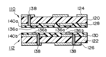
In this embodiment, two double-face PWB 110,
112 and four conductive layers 124, 128, 130, 126 are all
, .,
Z0067~76
previously processed by patterning. Each of the con-
ductive layers 124, 128, 130, 126 is a copper foil
having a thickness of about 18 - 35 ~m, for example.
Each of the double-face PWB 110, 112 has a
through-hole 138 at a predetermined position, the in-
ner surface of the through hole 138 being plated. The
through-hole 138 electrically connects front and rear
conductive layers 124, 128 or 130, 126 together.
A solder paste is printed on the conductive
layers 128, 130 of the double-face PWBs 110, 112 at
predetermined positions, or solder bumps 136a, 136b
are formed by solder reflow.
Then, a polymer resin 140a, 140b is printed on
the surface of the conductive layer 128, 130 at por-
tions devoid of the solder bump 136. A binder con-
tained in the polymer resin 140a, 140b is discharged
into the atmosphere so that the polymer resin 140a,
140b is precured.
As shown in FIG. 1, the foregoing components are
; placed one over another. Specifically, after the
polymer resin 140a, 140b have been precured, the two
double-face PWBs 110, 112 are placed one over another
in such a manner that the solder bumps 136a on one
double-face PWB 110 confront the solder bumps 136b on
the other double-face PWB 112.
Subsequently, these two double-face PWBs 110,
- 15 -
:
-.'
''
.
'',
2006'7'76
112 are processed by pressurizing and heating con-
currently. For example, the double-face PWBs 110, 112
are clamped between a pair of flat plates in the
direction of superimposing, under pressure and heat.
The flat plates are stainless steel, for example.
This pressurizing and heating are conducted
separately at first and second stages. At the first
stage, vapor-phase soldering is conducted at a
temperature, e.g., 220-C, higher than the melting
point of the solder bumps 136a, 136b for two minutes.
In this first stage, the solder bumps 136a, 136b are
fused to form fused solder bumps 142 (FIG. 2) which
electrically connect the conductive layers 128, 130
with one another. Meanwhile, the polymer resins 140a,
14Ob are brought in contact with one another due to
the reduced viscosity resulting from the temperature
rise and also due to pressure.
This first stage is-followed by the second
stage, in which the polymer resins 140a, 140b are
cured by heating at 150-C for about one hour. As a
result, a unitary insulating 144 (FIG. 2) has been
formed to insulate the conductive layers 128, 130 from
one another.
- From the foregoing steps, a composite PWB having
four conductive layers, namely, a four-layered PWB can
be obtained, as shown in FIG. 2.
-- 16 --
'.~
In this first embodiment, after the two double-
face PWBs 110, 112 have been superimposed into a unitary
form, it is unnecessary to form any through-hole, and the
PWBs 110, 112 may be previously processed by patterning.
Therefore, it is possible to avoid various
defects, such as inadequate smear, inadequate penetration
of plating liquid, etc., resulting from the forming of
through-holes. Also other imperfections due to
permeation of the liquid for patterning can be prevented.
lo Consequently, an improved rate of production of good
quality products can be achieved, thus minimizing the
occurrences of manufacturing troubles.
In addition, it is possible to use, as the
individual conductive layer, a copper foil having a
thickness smaller than the prior art. Therefore high-
concentration patterning and an improved degree of
circuit integration can be achieved.
A green sheet may be used instead of the
polymer resin 140a, 140b. The solder paste may be a
high-temperature or low-temperature paste now put on the
market, or may be an eutectic solder.
FIGS. 3 and 4 show various components for
manufacturing a multilayered PWB in a method according to
a second embodiment.
In the second embodiment, a conductiva layer
.,
:`:
,
,.,
- 17 -
`~ A
. .
2006776
228, 230 of each of two single-face PWBs 210, 212 is a
copper foil and is previously processed by patterning.
Firstly, a solder paste such as a eutectic
solder is printed on the conductive layers 228, 230 at
predetermined positions and is then reflowed to form
fused solder bumps 236a, 236b one on each conductive
layer 228, 230.
Then, the two single-face PWBs 210, 212 are
placed one over another in such a manner that their
respective solder bumps 236a, 236b confront one anoth-
er.
In this embodiment, copper balls 246a, 246b are
previously mixed in the respective printed solder
pastes. The rate of mixture of the copper balls 246a,
246b is determined depending on the coefficient of
reduction of the flux component of the solder paste
due to the reflow.
This state is shown in FIG. 3, from which state
pressure and heat, like the first embodiment, are ap-
plied to the components to form a fused solder bump
242. As a result, a double-layered PWB has been ob-
tained, as shown in FIG. 4.
In the second embodiment, in addition to the
results obtained in the first embodiment, it is pos-
sible to keep the distance between the conductive
layers 228, 230 constant, namely, equal to the
,
.,
- 18 -
~..
~006776
diameter of the individual copper ball 246. Con-
sequently, it is possible to prevent the solder bumps
236 from projecting, thus causing an improved pattern
precision and also a highly concentrated pattern.
Instead of being previously mixed in the solder
paste, the copper balls 246 may be placed on or may be
forcedly mixed in the printed solder paste or the con-
ductive resin processed by potting.
FIGS. 5 and 6 show various components for
manufacturing a multilayered PWB in a method according
to a third embodiment.
In this embodiment, a conductive resin 336 is
attached, by potting, on only one 330 of two conduc-
tive layers 328, 330 of two single-face PWBs 310, 312,
like the single-face PWBs in the second embodiment.
After the conductive resin 336 has been thus at-
tached on one conductive layer 330, ceramic balls are
forcedly mixed in this conductive resin 336.
FIG. 5 shows the single-face PWBs 310, 312 hav-
ing placed one over another in such a manner that the
conductive resin 336 attached on the conductive layer
330 by potting confronts a predetermined portion of
the conductive layer 328.
- As from the state of FIG. 5, the components are
pressurized in the superimposing direction under heat-
ing, the conductive resin 336 is cured to provide a
,:
`.
.... .
X006~7~
conductive adhesive portion.
In the third embodiment, the same results as the
second embodiment can be obtained.
Ceramic balls 346 may be previously either mixed
in or placed on the conductive resin 336.
In the second and third embodiments, the copper
balls 246 or the ceramic balls 346 are used; alterna-
tively, small pieces of a different shape may be used.
But the individual small piece should have a conctant
size in the direction of thickness to keep the inter-
substrate distance constant.
Small pieces of a d$fferent material, such as
iron or heat-resistant resin, may be used instead of
the copper balls 246 or ceramic balls 346.
FIGS. 7 and 8 show various components for
manufacturing a multilayered PWB in a method according
to a fourth embodiment.
In this embodiment, like the first embodiment,
solder bumps 436a, 436b are formed on conductive
layers 428, 430 of double-face PWBs 420, 422 at
predetermined positions, and polymer resins 440a, 440b
are attached on the double-face PWBs 420, 422,
whereupon these components are placed one over anoth-
er.
In FIG. 7, the components are shown after the
polymer resins 440a, 440b have been attached on the
- 20 -
2006776
double-face PWBs 420, 422 and also after these double-
face PWBs 420, 422 have been placed one over another.
As is seen from FIG. 7, there are following dif-
ferences, concerning the attaching of polymer resin,
between first and fourth embodiments. In the first
embodiment, the polymer resins 140a, 140b are attached
on the double-face PWBs 120, 122 so as not to lie over
the solder bumps 136a, 136b. In the fourth embodi-
ment, the polymer resins 440a, 440b are attached on
the double-face PWBs 420, 422 so as to lie over the
solder bumps 436a, 436b; the polymer resins 440a, 44b
should be a resin having a curing temperature lower
than the melting point of the solder bumps 436a, 436b.
When the components of FIG. 7 is pressed in the
superimposing direction by a predetermined pressure
and at the same time, is heated at a temperature high-
er than the melting point of at least the solder bumps
436a, 436b, the solder bumps 436a, 436b are fused ex-
cept the polymer resins 440a, 440b as the curint
temperature of the polymer resins 440a, 440b is lower
than the melting point of the solder bumps 436a, 436b.
As a result, the fused solder bumps 442 have been
:
formed to electrically connect the conductive layers
428, 430-. At that time, the polymer resins 440a, 440b
are in contact with one another as pressurized.
When the components are heated at the curing
..,
.,,
- - 21 -
.
,
~ '
Z006776
temperature of the polymer resins 440a, 440b, the
polymèr resins 440a, 440b is cured into a unitary form
to form a unified insulating layer 444.
As the foregoing steps are thus conducted, a
four-layered PWB of FIG. 8 has been manufactured.
In the fourth embodiment, the same results as
the first embodiment can be obtained. Additionally,
in this embodiment, the attaching of the polymer
resins 440a, 440b by printing can be conducted without
considering the portions to which the solder bumps
436a, 436b are attached. Therefore, with the fourth
odiment, it is possible to manufacture a multi-
layered PWB easily, compared with the first embodi-
ment.
FIGS. 9 and 10 show various components for
manufacturing a multilayered PWB in a method according
to a fifth embodiment.
In this embodiment, firstly a via hole 538 is
formed in a double-face PWB 520, and the inner surface
of the via hole 538 is plated. On the conductive
layer 530 of another PWB 522, the solder bump contain-
ing 2% of silver, 62% of tin and 36% of lead and hav-
:; :
ng a melting point of 179- is attached. Yet the
double-face PWB 520 and the PWB 522 are place one over
another in such a manner that this solder bump con-
fronts the via hole 538.
-
- - 22 -
:,
;-
: ~ '',.. " .` '' '
Z006'7~76
Then the via hole 538 and the solder bump areelectrically connected. In this embodiment, following
steps are adopted to electrically connect the via hole
538 and the solder bump.
Ultrasonic waves and a predetermined pressure
are applied over the double-face PWB 520 and the PWB
522 in the superimposing direction indicated by arrows
in FIG. 9.
At that time the ultrasonic waves causes the
temperature of the solder bump to rise. As the
temperature of the solder bump increases over its
melting point, the solder bump fuses to form a fused
solder bump 542. Accordingly the conductive layer 530
and the plated inner surface of the via hole 538 con-
fronting the conductive layer 530 are electrically
connected by the fused solder bump 542, whereupon ap-
plication of the ultrasonic waves is stopped. As a
result, a multilayered PWB electrically connected by
the fused solder bump 542 as shown in FIG. 9 has been
obtained.
- In the fifth embodiment, the same results as the
. ,.~,
-~ first embodiment can be obtained. Additionally, in
this embodiment, oxides 548 having formed on the con-
s~ ductive layer 528, for example, due to the heat is
dispersed more than directly heating, as shown in FIG.
~ 10. Therefore, the connection between the fused
:~ .
,...
` - 23 -
, .
':
~- ` ' ' ,
-
.~. : . , ' . .
:.
X0067'7~
solder bump 542 and the conductive layer 528 is firm,
thus causing a multilayered PWB which is resistant to
thermal shock and low in impedance between the sub-
strates.
An auxiliary direct heating concurrent with ap-
plication of the ultrasonic waves also causes the same
results.
FIGS. llA and llB show various components for
manufacturing a multilayered PWB in a method accord-
ingto a sixth embodiment.
In this embodiment, like the first embodiment,
the forming of solder bumps, the attaching of polymer
resins, the superimposing of the components, and the
pressurizing and heating are conducted. As a result,
a multilayered PWB (six-layered PWB) having a cross
section shown in FIG. llA has been obtained.
Further, the conductive layers are previously
; plated with platinum.
: As shown in FIG. llB, the surfaces of the con-
,
ductive layers 628, 630 are provided with platinum
layers 654, 656, respectively, having a thickness of
about O.S ~m by electroplating. Therefore the solder
bumps are formed on the platinum layers 654, 656.
In the sixth embodiment, the same results as the
first embodiment can be obtained. Additionally, it is
possible to prevent any circuit pattern from being
- 24 -
~006~76
ruptured due to the heat cycle, for example. Since
practically a PWB and a solder bump are different in
coefficient of thermal expansion, the conductive layer
would be subjected to a stress due to heat cycle, etc.
In this embodiment, any stress exerted on the conduc-
tive layers 628, 630 is buffered by the platinum
layers 654, 656 to thereby prevent any circuit pattern
from being ruptured due to such a stress.
In the illustrated embodiments, the conductive
layers are plated with platinum; alternatively, pal-
ladium may be used instead of platinum for the same
results.
Further, in the foregoing embodiments, the mul-
tilayered PWB has a relatively small number of layers.
But it may have a larger number of layers.
The foregoing description concerning the multi-
layered PWB may be said for a multilayered PCB. For
, example, as shown in FIG. 12, it is possible to
manufacture a multilayered PCB in which circuit ele-
ments 758, 760 have been installed on or in the super-
imposed layers in the same method as the sixth embodi-
ment.
.'
:
- 25 -
'
''
, .,
::.